OATAO is an open access repository that collects the work of Toulouse
researchers and makes it freely available over the web where possible
Any correspondence concerning this service should be sent
to the repository administrator:
[email protected]
This is an author’s version published in:
https://oatao.univ-toulouse.fr/24285
To cite this version:
Erroui, Najoua and Gateau, Guillaume and Roux, Nicolas. Full
wave modulation applied to 3-level FC and NPC inverters
(2019). In: 2019 IEEE International Conference on Industrial
Technology (ICIT), 13-15 February 2019 (Melbourne,
Australia)
Official URL:
https://doi.org/10.1109/ICIT.2019.8755070
Full wave modulation applied to 3-level FC and
NPC inverters
Najoua Erroui, Guillaume Gateau, Nicolas Roux
LAPLACE, Université de Toulouse, CNRS, INPT, UPS, France 2, rue Charles Camichel - BP 7122 - 31071 Toulouse cedex 7
France Abstract— The multi-level converters are more and more used for high power medium voltage applications. They seem to be the best option to reduce the weight of the converter and still have high efficiency. However, they should be used with an adapted control strategy to reduce their power losses that could be high due to the used high switching frequencies and also to improve the output harmonics quality. The commonly used PWM strategy can lead to high switching losses and less output harmonic content in comparison with full wave modulation. This paper aims to explain the limits of PWM modulation for our application and the advantages of full wave modulation adapted to multilevel converters. These control strategies will be compared for 3-level FC, and 3-level NPC topologies and their effect on the converter weight and performances will be studied to find the most interesting solution regarding specific power and inverter efficiency.
Keywords— Multilevel converter, modulation, control strategy, specific power, power losses,
I. INTRODUCTION
This work takes part into HASTECS project [1] which aims to optimize the complete electrical chain of the hybrid aircraft integrating all aeronautical constraints such as partial discharges for electrical equipment placed in the non-pressurized zone or, in case of high operating voltage, even in the pressurized area. HASTECS project has set itself the challenge of doubling the specific power of electric machines including their cooling, while the power electronics, with their cooling system, would evolve from 15 kW/kg in 2025 using only Silicon semiconductors to 25 kW/kg in 2035 using wide bandgap components. Inverter topologies, control and modulation strategies and also semiconductor technologies will be taken into account to find the optimal structure which meets the specific power and efficiency targets.
The main objective of this work is to evaluate several power converter architectures and associated control strategies to power an electric machine used for aircraft propulsion. A comparative study of modulation topologies and strategy was carried out to highlight the structure and modulation presenting the best performance to minimize the losses for the sizing point.
This paper mainly focuses on full wave modulation and the results comparison with sinusoidal pulse width modulation (PWM) that is commonly used. The calculation of converter losses, using these modulation strategies, were determined by simulation in PLECS and then integrated into the MATLAB design Tool [1].
Given our application, only three-level converter topologies will be studied using different full-wave and PWM controls. The studied converter topologies are:
• Neutral Point Clamped (3-level NPC) • Flying Capacitor (3-level FC)
II. INVERTER DESIGN USING PWM
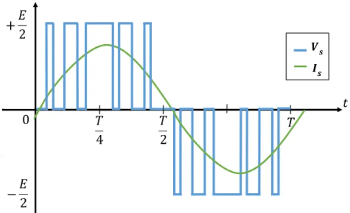
In order to have a point of reference, results using the PWM are given. Modulation strategies aim to get an output voltage that approximates a sinusoidal wave with adjustable amplitude or frequency. Each strategy has its switching configuration which generates control reference and keeps the voltage sources balanced. The output desired voltage and current are shown in Fig. 1.
The multilevel modulation techniques could be classified according to switching frequency [2]. High switching frequency modulations have higher switching losses and less output harmonic content than fundamental ones. Therefore, with low switching frequency methods, the efficiency is higher.
Fig. 1 : Output desired voltage and current 3-level PWM waveforms +𝐸 2 −𝐸 2 0 𝑡 𝑇 2 𝑇 4 𝑇 𝑽𝒔 𝑰𝒔
Sinusoidal PWM is the most popular method where a high-frequency triangular carrier wave is compared with a sinusoidal reference of the desired frequency. The intersection of both waves defines the switching or commutation instants. For this modulation, the harmonics are around the switching frequency, and this was the method used so far for this project [3].
Two sizing cases are to be considered. The first one consists of sizing the inverter for the takeoff (maximum power of the profile: 1 MW) and study its performances for the cruise (0.5 MW). For the second one, the inverter is sized for the cruise which represents the most extended flight phase. The latter is the one used in this paper.
Using the PWM and the topologies described in the following parts, 3-phase inverter performances for the takeoff power point with the cruise sizing point is given in Table 1.
To estimate the inverter specific power including the heat exchanger, a 0.4 kW/kg coefficient is taken into account which translates the losses directly into cooling system weight. The passive components weight, capacitors in this case, are also taken into account.
Table 1 : 3-level FC and NPC performances at 1 MW with 2 kV DC bus
Topology FC NPC 𝜂(%) 98.83 98.86 Losses (kW) 11.81 11.49 Maximal junction temperature (°C) 141 152 Specific power (kW/kg) 11.03 19.20
The maximal junction temperature of the NPC components is higher than the silicon limit specified by the component manufacturer which is 150°𝐶. To cross this point without exceeding the thermal limit, the inverter should be sized for the maximal power, but its performances will not be optimized for the cruise.
Fig. 2: Conduction and switching losses for 3-level FC and NPC
The switching losses account for a significant amount of the total power losses in this type of inverters as in Fig. 2. Unlike conduction losses, they can be reduced by reducing the switching frequency without reducing the current or changing the used component parameters.
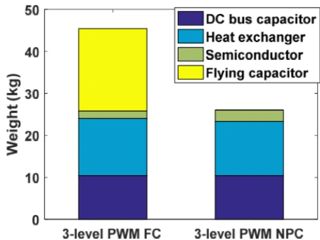
Fig. 3 presents the weight distribution for both topologies. The cooling system represents a large part of the mass. Reducing the cooling requirements by reducing the losses in the converter would decrease the global weight of the system, also reducing its physical size and manufacturing cost. It would also increase the specific power. The switching loss minimization can be done by using a full wave modulation.
Fig. 3 : Weight distribution (kg) for the studied topologies for sizing power point 0.5 MW
The reduction of switching frequency generally causes an increase in harmonic distortion of the line- and motor-side waveforms of the drive which will be the case of the full wave modulation. THD must be monitored.
III. NEUTRAL POINT CLAMPED (NPC) A. Topology
The neutral point clamped inverter employs clamping diodes and cascaded DC capacitors to produce alternative voltage waveforms with multiple levels. The inverter can generally be configured as a 3, 4, or 5-level topology, but only the three-level inverter has found wide application in medium voltage high power drives [5] [6]. The 5-level NPC topology is not used because of the complexity of the clamping diode circuit. The following figure (Fig. 4) represents one leg of the 3-phase 3-level NPC inverter.
This structure is based on a direct series association by adding a clamp to fix the switches voltage allowing to divide the input voltage.
This structure does not improve the inverter output apparent switching frequency, and the clamping circuit is a little complex to realize. 3-level PWM FC 3-level PWM NPC 0 2 4 6 8 10 12 Conduction Switching
The main advantage of this structure is the reduced and output harmonics compared to the two-level inverter working at the same voltage rating and switching frequency. But it needs additional clamping diodes, intricate PWM switching pattern design, and possible deviation of the neutral point voltage which should be taken into account using this structure [7]. B. Full wave modulation
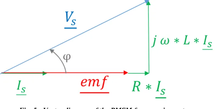
A three-phase 3-level NPC inverter supplying a 𝑅 𝐿 load in series with a sine electromotive force (EMF), with a power of 1 MW, to represent the synchronous machine (PMSM) developed by one of the HASTECS project work packages [8] is controlled using a full wave modulation as in Fig. 5.
Fig. 5 : Vector diagram of the PMSM for a maximum torque 𝑉 = 𝑅 ∗ 𝐼 + 𝑗𝐿 𝜔 𝐼 + 𝑒𝑚𝑓 (1) 𝑒𝑚𝑓(𝑡) = Φ _ ∗ 𝜔 ∗ sin (𝜔𝑡) (2)
With 𝑅 and 𝐿 the stator resistance and inductance and Φ _ the no load flux and the electric pulsation.
The considered full wave modulation is a 3-level wave (+E/2,0,-E/2) in which, the 0 level duration is used to control the supplied RMS voltage (𝑉 ) or amplitude value (𝑉 ), with 𝐸 the DC bus voltage value (Fig. 6).
𝛼 = ∗ 𝑎𝑠𝑖𝑛(
∗ ) (3)
To obtain this output voltage waveform, the two switching cells’ control signals are issued of comparison of a constant 𝛼 (3), and a low-frequency triangular wave for the first cell and a half a period delayed triangular wave for the second cell. The first switching cell is consisting of components T1 and T3 and the second one T2 and T4. The switches of a switching cell have complementary states (𝑇3 = 𝑇1 , 𝑇4 = 𝑇2) as shown in Fig. 7.
Fig. 7 : Switching cell command schematic
The generated control signals are shown in the following figure (Fig. 8).
Fig. 8 : T1 and T2 3-level NPC control signals
This modulation will generate the desired voltage and current waveforms (Fig. 6) with only low-frequency switching which will reduce the overall power losses of the inverter. Simulation results will be presented in the last part of this paper.
𝑉
𝑗 𝜔 ∗ 𝐿 ∗ 𝐼
𝑒𝑚𝑓
𝐼
𝑅 ∗ 𝐼
φ
Fig. 4 : Single leg 3-level NPC inverter
IV. FLYING CAPACITOR (FC) A. Topology
The flying capacitor inverters have evolved from the two-level inverter by adding DC capacitors to the cascaded switches [9]. There are two complementary switch pairs in each leg of the 3-level inverter. The flying-capacitor inverter in Fig. 9 can produce an inverter phase voltage with three voltage levels.
This structure is based on a direct series association by adding an intermediate floating source to fix the switches voltage and allows to split the input voltage by combination. In this case, it is necessary to guarantee the balancing of the voltage of the flying capacitor.
More than one switching state can obtain some voltage levels. The 0 voltage level, for instance, can be produced by two sets of different switching states. The switching state redundancy is a common phenomenon in multilevel converters, which provides great flexibility for the switching pattern design.
This structure thus makes it possible to divide the sizing voltage of the switches, to increase the output apparent switching frequency and, as a consequence, to reduce the current ripple or the size of the inductance at the output, which makes it possible to improve the output performances.
Fig. 9 : Single leg 3-level FC inverter
The FC is also a multilevel inverter, producing the voltage waveforms with lower and THD than a regular two-level inverter. However, the flying-capacitor inverter has some drawbacks such as a large number of capacitors and their voltage balancing issues.
B. Full wave:
As for the 3-level NPC topology, a three-phase converter that supplies an 𝑅𝐿 load in series with a sine electromotive force is studied.
Various control strategies have been implemented to improve the operation, loss distribution and voltage regulation of the flying capacitor.
In this study, the converter is studied using perfect voltage sources instead of flying capacitors assuming that the voltage of the flying capacitor is perfectly controlled.
1) Full wave 1
For the full wave control called "Full Wave 1", the control of both switching cells are centered, and the duty cycle is chosen to control the RMS voltage value.
To obtain the output voltage waveform the two switching cells’ control signals are issued of comparison of a constant (1 − 𝛼) (3), and a low-frequency triangular wave for the first cell and the triangular wave is compared to 𝛼 for the second cell. The first switching cell is consisting of components T1 and T3 and the second one of T2 and T4. The issued control signals are similar to the NPC ones (Fig. 8).
Fig. 10 : Full wave 1 used switches combination
For this modulation, a fixed combination of switches was chosen for the 0 voltage level bearing (Fig. 10). This method unbalances the losses of the switches of this topology, which prevents us from taking advantage of one of the key strengths of this structure, which is the balanced distribution of losses.
For a DC bus voltage of 2 kV, a load power of 1 MW, the needed flying capacitor value is 6.08 mF which is more important than the DC bus capacitor of 2.5 mF. In this case, the flying capacitor is sized according to the low-frequency component of the current.
2) Full wave 2
The second modulation idea consists of adding to the "Full Wave 1" command, the combination of the two possible configurations for the 0 voltage level (Fig. 11), and thus be able to balance the losses of the two switching cells over two periods.
The full wave control called "Full Wave 2" is designed as over a first period, switch T1 is primed, and T2 is blocked to create the voltage level at 0 V, and in the following one, switch T2 is primed, and T1 is blocked to generate the 0 V. This command, therefore, balances the losses in the switches over two periods.
Fig. 12 : T1 and T2 3-level FC full wave 2 control signals For this modulation, the flying capacitor sizing does not change. The value remains high and can only be reduced by increasing the switching frequency.
3) Full wave 3
Following the idea of the previous case, as to improve the losses balancing over a single period, but with a smaller flying capacitor, the “Full Wave 3” was developed. It consists in switching the two switches combinations (over the same period) in high frequency to make the output voltage level at 0 𝑉 as an average of opposite voltages applied the same amount of time. It allows a reduction of the size of the flying capacitor and at the same time maintain its voltage at an average value of
.
Fig. 13 : Voltage and current waveforms for 3-level FC using full wave 3 for a switching frequency of 60 kHz
To maximize the reduction of the flying capacitor weight, the 0 V level could be achieved by switching at a high frequency of 6 kHz which corresponds to 10 times the electrical machine frequency. This switching frequency engenders a flying capacitor of 1.3 mF as for the PWM strategy.
In this case, using a 6 kHz switching frequency will not be interesting due to the high value of the electrical machine frequency (600 Hz) and the duration of the 0 V level which is
very short ( − 𝛼 ∗ 𝑇 with 𝛼 = 0.45). The ratio between the two frequencies must be higher for this method to be interesting.
For the 6 kHz one, the 0 level does not appear to include changes of state. To have more than two commutations, the switching frequency should be higher than 27 kHz. That is why, a second example is given in Fig. 13 with a switching frequency of 60 kHz. This switching frequency engenders a flying capacitor of 0.13 mF.
V. RESULTS A. Efficiency and power losses comparsion
For a DC bus voltage of 2 kV, a load power of 1 MW and a switching frequency of 6 kHz, the performances using full wave modulation for both topologies are compared to a regular PWM.
To estimate the inverter specific power, the heat exchanger, capacitors and semiconductor weights are taken into account.
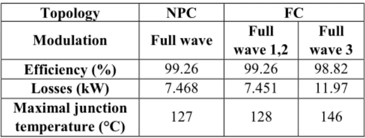
Table 2 : Full wave comparison for 3-level NPC and FC for P = 1 MW
Topology NPC FC
Modulation Full wave wave 1,2 Full wave 3 Full Efficiency (%) 99.26 99.26 98.82
Losses (kW) 7.468 7.451 11.97 Maximal junction
temperature (°C) 127 128 146
Using the full wave modulation, the losses are lower due to the reduction of switching losses as it can be noticed in the following figure.
For the FC topology, the size of the flying capacitor puts this topology at a disadvantage for both modulations, PWM and full wave. However, using full wave 1 or 2 methods generate a higher flying capacitor weight as seen before.
Fig. 14 : Conduction and switching losses for 3-level FC and NPC using full wave modulation
FC full wave 1 FC PWM NPC full wave NPC PWM 0 2 4 6 8 10 12 Conduction Switching
B. Total harmonic distortion
Regarding the current total harmonic distortion (THD) calculated as in (4), it is equal to 3.6% for PWM while for full wave it is equal to 4.4% for NPC and FC 1 and 2 and 6.9% for full wave 3 with a switching frequency of 15kHz and 4.8% for 60 kHz. The current generated using the full wave modulation has a similar waveform to the PWM one as it can be noticed in Fig. 15.
𝑇𝐻𝐷 = (4)
With 𝐼 the current fundamental amplitude and 𝐼 the harmonics amplitude.
Fig. 15 : Current waveforms and THDs for 3-level FC using full wave 1 and PWM for P = 1 MW
The full wave modulation, in the studied case, does not alter the THD unlike what was expected. This is due to the used synchronous machine properties.
VI.CONCLUSION
This project aims to create a high specific power inverter with high efficiency. Even by using multilevel topologies, the power losses are still high due to the high switching frequency so is the cooling system. So to reduce the converter weight and improve its efficiency, low-frequency modulation is suggested. The full wave modulation studied in this paper is applied to 3-level NPC and FC. As expected, this control strategy reduced the switching power losses and overall the converter weight due to the reduction of the heat exchanger size. However, it did not deteriorate the output current THD. For the 3-level FC topology, it has a significant impact on the flying capacitor size that should be taken into account if this solution is chosen.
The heat exchanger weight could be decreased if the inverter is sized using the full wave modulation since the losses will be lower. The losses are almost divided by two using the full wave compared to the PWM ones for the same power point. However, the use of full wave modulation for the whole mission profile could be interesting and will be studied for the other flight phases for the project next steps.
For the FC topology using full wave modulation, the study was realized using perfect voltage sources instead of flying capacitors. Flying capacitors’ voltage balancing should be taken into consideration. The 0 voltage level phase of the output voltage can be used to balance the flying capacitor voltage at high frequency actively.
ACKNOWLEDGMENT
This project has received funding from the [European Union’s Horizon 2020 (cleansky 2 JTI) research and innovation program, 2014-2024] under grant agreement No 715483
REFERENCES
[1] N. Erroui, G. Gateau, and N. Roux, “Continuous-caliber semiconductor components,” in 2018 IEEE International Conference on Industrial Technology (ICIT), 2018, pp. 658–663.
[2] J. Rodriguez, Jih-Sheng Lai, and Fang Zheng Peng, “Multilevel inverters: a survey of topologies, controls, and applications,” IEEE Trans. Ind. Electron., vol. 49, no. 4, pp. 724–738, Aug. 2002.
[3] M. Ibrahim, “High Power Conversion System for Aircraft Hybrid Propulsion: Multilevel Converters Design Conception, Analysis Study, and Optimization,” Laboratoire Laplace, Toulouse, France, 2016, unpublished.
[4] B. Wu and M. Narimani, High-Power Converters and AC Drives. John Wiley & Sons, 2017.
[5] J. Shen and N. Butterworth, “Analysis and design of a three-level PWM converter system for railway-traction applications,” IEE Proc. - Electr. Power Appl., vol. 144, no. 5, pp. 357–371, Sep. 1997.
[6] Y.-H. Lee, B.-S. Suh, and D.-S. Hyun, “A novel PWM scheme for a three-level voltage source inverter with GTO thyristors,” IEEE Trans. Ind. Appl., vol. 32, no. 2, pp. 260–268, Mar. 1996.
[7] B. Wu and M. Narimani, High-Power Converters and AC Drives. John Wiley & Sons, 2016.
[8] S. Touhami, Y. Bertin, Y. Lefèvre, J. F. Llibre, C. Henaux, and M. Fénot, “LUMPED PARAMETER THERMAL MODEL OF PERMANENT MAGNET SYNCHRONOUS MACHINES,” p. 6, 2017.
[9] M. F. Escalante, J. C. Vannier, and A. Arzande, “Flying capacitor multilevel inverters and DTC motor drive applications,” IEEE Trans. Ind. Electron., vol. 49, no. 4, pp. 809–815, Aug. 2002.
PWM Full wave
Full wave PWM