THÈSE
En vue de l'obtention duDOCTORAT DE L’UNIVERSITÉ DE TOULOUSE
Délivré par l’Université Toulouse III– Paul SabatierDiscipline ou spécialité :Microondes, Électromagnétisme et Optoélectronique
JURY
Pr. Jean-Guy TARTARIN (Directeur) Pr. Jacques GRAFFEUIL (Président de Jury)
Pr. Jean-Claude DE JAEGER (Rapporteur) Mcf. Olivier LATRY (Rapporteur) Pr. Frédéric MORANCHO (Examinateur) Mcf. Arnaud CURUTCHET (Examinateur)
Ing. Christian MOREAU (Invité) Dr. Benoit LAMBERT (Invité)
Ecole doctorale : GEET
Unité de recherche : LAAS-CNRS, groupe MOST Directeur de Thèse : Jean-Guy TARTARIN Présentée et soutenue par Serge KARBOYAN
Le 04 Octobre 2013
Titre : Dedicated Design Of Experiments and Experimental Diagnostic Tools for Accurate Reliability Investigations on AlGaN/GaN High Electron Mobility
I would like to sincerely thank the successive directors of LAAS – CNRS, Prof. Raja CHATILA, Prof.
Jean-Louis SANCHEZ (for whom I pay homage) and Prof. Jean ARLAT, allowing me to achieve this work
in their institute. Moreover, I also wish to express my gratitude to Prof. Olivier LLOPIS, the head of
Microwave and Optomicrowave System for Telecommunications (MOST) team.
This work is funded by the ANR (Agence National de la Recherche) within the project entitled
ReAGaN (Reliability Analysis of GaN devices). Thus, it is worth remembering all our partners from TRT,
UMS, IMS, Lepmi and Serma as well as their contribution to this work. Moreover, the French Department
of Defense took also a part from this project. I take this opportunity to acknowledge them all for providing
financial assistance, deep discussions and teamwork accomplished together.
The road to my Ph.D. ended on October 4
th, the “big day” as everyone was saying. I would like to thank
the committee members, Prof. Jean-Claude DE JAEGER and Mcf. Olivier LATRY for their deep review
despite the constraints and the short time provided to them, as well as for their insightful questions. Thank
you again ! In addition, I can never forget the deep discussions with Christian MOREAU, Eng. Of the
French DoD, and his valuable answers to my questions; moreover, the presence of Dr. Benoit LAMBERT
from UMS was a big support for my thesis and for the project. My deepest acknowledgments go to Prof.
Jacques GRAFFEUIL, head of my thesis committee and for whom I will come back later. I would also
thank Prof. Frederic MORANCHO and Mcf. Arnaud CURUTCHET for being part of my committee and
for your helpful comments.
The input of my colleagues at LAAS – CNRS has been very valuable. Your door was always open to
discuss and advice everything. With no doubt, your kind contributions must be recognized. I will not
mention you one-by-one, but when reading this, you will recognize yourself. I can never forget the deep
discussions with my office-mate Seraphin, the help of Laurent BARY with the LFN bench and the big
support of Alexandre RUMEAU on the Cryoprober mainly.
I gratefully thank all the staff and services at LAAS – CNRS. Many thanks Christian BERTY and
Dominique DAURAT for your patience and the library staff, for your cooperation. Moreover, I am grateful
to Brigitte DUCROQ, Marie ESTRUGA and Sophie COBOURG for your administrative support and for
being helpful every time with a big smile.
The biggest support in France was through the Lebanese community; it is through those people that I
loved France and living in this beautiful country ! The word “thank you” is not enough for you my
Lebanese fellow-mates.
And here comes to the special acknowledgements…
At this moment of accomplishment, I am extremely indebted to my supervisor and my advisor
Prof. Jean-Guy TARTARIN. I successfully overcame many difficulties and learned a lot from your
guidance, support and encouragement. You encouraged me not only to grow as an experimentalist and a
physicist but also as a self-instructor and a particular independent thinker. I hope - in the future - to
continue to work with your noble thoughts.
It is extremely hard to convey my deep sense of gratitude to you in words: I will forever be thankful to
Prof. Jacques GRAFFEUIL. You were very helpful, gracious and amazing to me. You directed me through
various situations, allowing me to reach this accomplishment.
Some friends really deserve to be mentioned: Dina, Lara, Zeina, Ayad, Charbel, Hagop and Khaldoun.
Simply, you are part of my family. Thank you for your support and help during the difficult moments,
mainly, for never leaving my side. “You are a sweet responsibility and never an opportunity” Happy ?
It is my fortune to gratefully acknowledge the support of my family members. From my first day abroad
their sleeping hours decreased, their dreams became shorter and their life became harder. Having you in my
life is an honor, your profound understanding is an encouragement and your support is unconditional. I
believe that you gave up many things for me to be here today. To you, I am eternally grateful and thankful.
Well, we think that this is the end, but it is only the beginning. But be sure, you, special people, you are
my beginning and my end and is for you that I dedicate this work.
It is the end of the Acknowledgement, and here I wish you courage if you dare to continue to the next
pages.
Serge KARBOYAN
Toulouse, France
October, 2013
Le développement intensif et rapide des dispositifs HEMT à base de nitrure de gallium a été largement favorisé par les qualités intrinsèques du matériau pour proposer des performances élevées (haute puissance, haute fréquence…) et pour autoriser un fonctionnement en environnement extrêmement sévère (fluctuations thermiques, brouillage, tenues aux radiations ionisantes…) par rapport aux technologies concurrentes plus traditionnelles (Si, GaAs…). À ce jour, les dispositifs HEMTs AlGaN/GaN sont considérés comme une alternative prometteuse pour remplacer la technologie GaAs, et se positionnent comme d’excellents candidats pour des applications d'électronique de puissance, pour les applications TVSAT, des stations de base terrestres et des systèmes radar à large bande de fréquence (bande L à W), et pour les applications civiles et militaires. Cependant, il reste à lever certains verrous concernant des problèmes de fiabilité de ces dispositifs, qui affectent la durée de vie élevée attendue ; l'amélioration de la robustesse de ces technologies reste une phase critique à étudier malgré les progrès déjà réalisés. Plusieurs paramètres de fabrication affectent la fiabilité, tels que la passivation de la surface, le plateau de champ, le procédé de dépôt de la grille. Il est bien connu que l’étude de la fiabilité est complexe et ne pourra jamais être totalement accomplie, cependant les limites escomptées pour une exploitation raisonnable des filières GaN laissent entrevoir la possibilité de réels progrès dans ce domaine pour assoir le positionnement de ces technologies vis à vis des solutions concurrentes. Ce manuscrit de thèse présente les outils de diagnostic et les procédures de mesures associées développés pour mieux comprendre les mécanismes de dégradation sous-jacents de ces dispositifs. Les mesures électriques DC et pulsées à différentes températures sont présentées en premier lieu. Pour obtenir des informations au niveau microscopique sur la fluctuation des porteurs et des défauts dans les zones actives et passives du dispositif, des mesures de bruit basse fréquence sont effectuées sur les courant de grille et de drain sous différentes configurations : la diode seule (drain en l’air) et le transistor en régime saturé. Une technique électro-optique, l’OBIRCh (Optical Beam Induced Resistance Change technique), est aussi appliquée sur les mêmes composants : cette technique apporte d'autres informations quant à l'intégrité du composant (fluctuations de courant), et vient corroborer nos hypothèses sur l’activation de mécanismes piezoélectriques dans les zones fortement polarisées du composant.
Toutes ces techniques non-destructives permettent des analyses croisées. Un modèle original de la diode Schottky a été établi pour tenir compte de certains défauts d'homogénéité à l'intérieur du contact de grille à l'interface entre la diode Schottky et la couche semi-conductrice supérieure. D'autres résultats originaux ont été trouvés à partir des mesures de bruit basse
fréquence concernant la localisation des défauts actifs et leur évolution suite à l’application d’un stress électrique et thermique (HTRB, HTOL, …). Les analyses électriques (pulsées et transitoires) des phénomènes de retard à la commande (grille ou drain) sont partiellement corrélées aux analyses du bruit basse fréquences des courant de grille et de drain pour identifier les mécanismes sous-jacents de dégradations. Dernièrement, une ébauche de plan d'expérience (DOE) est proposée dans le cadre de notre travail, qui complètera celui mis en œuvre dans le cadre du projet ANR REAGAN impliquant tous les partenaires : des règles et des procédures expérimentales sont identifiées pour s'assurer que les données expérimentales sont fiables (i.e. reflètent statistiquement le comportement réel du dispositif).
PAE, high frequency, moderate HF noise…) and for operating under different extreme conditions and harsh environment (thermal fluctuations, jamming, ionizing radiations…) over more traditional competitive technologies (Si, GaAs). More than ever, AlGaN/GaN HEMTs are considered as promising technology to replace the GaAs, and an excellent candidate for power electronics applications, for TVSAT applications, terrestrial base stations and radar transceivers operating over large frequency band (from L to W-band) for both civil and military applications. However, some remaining problems concerning the reliability of the devices affect the expected elevated lifetime, and the improvement of the robustness of these technologies stay a questionable phase to study despite the progress already made. Several fabrication parameters could impact the reliability such as surface passivation, field plate, gate deposition process (presence of spontaneous and piezoelectrical effects). It is well known that the reliability background is complex and will never be completely accomplished, but the margin between expected theoretical lifetime and results already obtained motivates efforts to give for an improved level of reliability. The following manuscript presents diagnostic tools and associated measurement procedures to better understand the underlying degradation mechanisms of such devices. Electrical DC and pulsed measurements at different temperatures are presented first. To get more microscopic information about the carrier flow and the defects in the active and passive areas of the device, low frequency noise measurements on the gate and drain currents are investigated under open drain (Schottky diode) and when the transistor is biased in saturated region. An electro-optical technique is also applied, called OBIRCh (Optical Beam Induced Resistance Change technique), on the same devices: this technique brings other expertise about the device integrity (current fluctuations).
All these non-destructive techniques are cross-correlated. Original Schottky diode models have been established to account for some inhomogeneities within the gate contact at the interface between the Schottky diode and the upper semiconductor layer. Some other original results have been found from Low Frequency Noise measurements concerning the location of the active defects, and their evolution after the application of thermal and electrical stresses (HTRB & HTOL). The electrical (pulsed and transient) analyses of lag effects are correlated to the harmonic low frequency analysis of the current spectral densities to identify the root trapping mechanisms. Lastly, a first Design of Experiment (DOE) is proposed in conjunction with our work, and also within the ANR REAGAN project involving all the partners: experimental rules and procedures are identified to ensure that the experimental data are reliable (i.e. reflect the actual behavior of the device, with statistical assessment).
I.1 INTRODUCTION ... 3
I.2 HISTORY, ECONOMIC AND MARKET RELEVANCIES ... 4
I.2.1 History ...4
I.2.2 Economic and market relevancies ...5
I.2.3 Applications ...7
I.3 WIDE BANDGAP SEMICONDUCTORS: ELECTRICAL PARAMETERS ... 8
I.3.1 Bandgap ...8
I.3.2 Surface mobility ...9
I.3.3 Breakdown voltage...9
I.3.4 Figure of merits for power modules ... 10
I.4 HEMT DEVICES ... 11
I.4.1 General information ... 11
I.4.2 GaN versus GaAs and InP power HEMTs ... 13
I.4.3 Gate access: Schottky contact and gate current carrier transport ... 14
I.4.3.a Schottky contacts ... 14
I.4.3.b Gate current carrier transport ... 14
I.4.4 Drain and source accesses: Ohmic contacts ... 17
I.5 GAN TECHNOLOGY: A MATTER OF ELECTRO-MECHANICO-THERMAL MANAGEMENT ... 17
I.5.1 Piezoelectric and spontaneous polarizations ... 17
I.5.1.a Piezoelectric polarization ... 17
I.5.1.b Spontaneous polarization ... 18
I.5.2 Thermal management ... 20
I.6 STRESSES ... 21
I.6.1 Arrhenius accelerated lifetime testing ... 21
I.6.2 DC stresses ... 22
I.6.2.a High Temperature Reverse Bias (HTRB) stress ... 23
I.6.2.b High Temperature Operating Life (HTOL) stress ... 23
I.6.2.c IDQ stress ... 23
I.6.2.d Step stress ... 24
I.7 RELIABILITY OF GAN DEVICES ... 25
I.8 DEGRADATION MECHANISMS AND RELIABILITY CONCERNS ... 28
I.8.1 Electromigration (EM) ... 28
I.8.3 Hot carriers and trapping/detrapping effects ... 32
I.8.3.a Surface traps ... 33
I.8.3.b Substrate traps ... 33
I.8.4 Metallurgical degradation and interface inhomogeneities ... 33
I.8.5 Electrostatic Discharge (ESD) ... 33
I.9 CONCLUSIONS ... 34
I.10 REFERENCES ... 36
CHAPTER II:DESIGN OF EXPERIMENTS AND CHARACTERIZATION PROCEDURES FOR PHYSICAL AND ELECTRICAL ANALYSIS AT THE DEVICE SCALE ... 40
II.1 INTRODUCTION ... 40
II.2 REAGAN PROJECT: DESCRIPTION, SCIENTIFIC AND TECHNICAL OBJECTIVES... 41
II.3 EXPERIMENTAL PROCEDURES DEVELOPED IN LAAS AND DEDICATED TO THE RELIABILITY ANALYSIS ... 46
II.3.1 Electrical DC and pulsed characterization (versus temperature)... 47
II.3.1.a Gate current study ... 47
II.3.1.b Drain current study ... 50
II.3.2 Pulsed time-domain measurements ... 52
II.3.3 Low frequency noise measurement ... 53
II.3.3.a Noise sources involved in GaN HEMTs ... 54
II.3.3.b Different noise sources ... 55
II.3.3.c Adjustment of the measurement bench [16] ... 60
II.3.4 Deep level Transient Spectroscopy (DLTS) technique ... 65
II.3.4.a Definition ... 65
II.3.4.b Emission and capture processes of deep centers ... 65
II.3.4.c Principle of DLTS ... 66
II.3.5 OBIRCh: an electro-optical technique ... 67
II.3.5.a Laser stimulation technique ... 67
II.3.5.b Description of the technique ... 67
II.3.5.c Implementation ... 70
II.4 CONCLUSIONS ... 70
II.5 REFERENCES ... 72
CHAPTER III:RELIABILITY STUDY CASES ... 75
III.1 INTRODUCTION ... 75
III.2 GH50DECLINATION_S: ON WAFER DEVICES ... 76
III.2.1 Devices under test and study roadmap ... 76
III.2.2 Electrical characterization versus temperature ... 78
III.2.2.a Electrical parameters extraction ... 79
III.2.2.b Potential fluctuation model application ... 82
III.2.3 Gate LFN characterization ... 85
III.2.4 OBIRCh results on Declination_S devices ... 91
III.2.5 Mechanical and piezoelectrical stresses in the devices ... 92
III.3.3 Pulsed time-domain measurements ... 107
III.3.4 Gate and drain LFN characterization ... 109
III.3.4.a Gate LFN characterization ... 109
III.3.4.b Discussion on the gate LFN characterization of Declination_S and Declination_L devices 113 III.3.4.c Drain LFN characterization ... 115
III.3.5 OBIRCh results on Declination_L devices ... 119
III.3.6 Deep level trap study: I-DLTS ... 122
III.4 CONCLUSIONS ... 124
III.5 REFERENCES ... 126
GENERAL CONCLUSION ... 130
1 The needs for high power amplification at high frequencies are increasing for both military and civil applications. For military applications, they are focused on RADAR and communication systems, and for civil applications the market is competing for the most reliable and powerful wireless telecommunications and base stations. At last, the space applications (civil or military) are also concerned for the fabrication of satellites, base stations and radar systems for GPS tracking, meteorological applications, etc. All these applications require high power levels, high linearity and high frequencies for enhanced data rates. Thus, these requested features have led to the study of wide bandgap technologies and more precisely the Gallium Nitride (GaN).
The deep studies on the GaN technology restarted in the 90s. The semiconductor was considered very interesting due to its wide bandgap (to reach high voltages and high carrier densities), high saturation velocity of the carriers (to reach high current values at high frequencies), high breakdown voltages and excellent thermal management (allowing the semiconductor to evacuate the maximum calories more efficiently than the conventional GaAs). These properties give the Field Effects Transistors (FETs) robustness and performance required for applications at high power and high frequencies. Consequently, the high electron mobility transistors AlGaN/GaN fabricated within the GaN technology showed the same qualities added to this the high electron mobility in the 2DEG. However, with all these qualifications, the GaN-based HEMTs still suffer of reliability issues and need more investigations and failure analysis to stand as alternative solution for GaAs and Si technologies. The work presented in this thesis is performed at LAAS – CNRS in Toulouse, France and is a part of ReAGaN - ANR project assembling six partners (UMS, IMS, TRT, LEPMI and SERMA) and the DGA French DoD (Department of Defense). The project addresses the reliability of the GaN technology in its industrialization phase. Its main objective is the development of advanced electro-optical and physical characterisation techniques dedicated to wide bandgap semiconductor technologies. For the first time, new analysis techniques are developed and their results are correlated leading to the identification and characterisation of nano-structural defects and physical mechanisms taking place in GaN technologies and potentially responsible for degradation.
Assuming the project and since this work is a part of it, hence this manuscript is organized around two main complementary axes.
2 The first axe consists of developing several original characterization procedures for the evaluation of AlGaN/GaN HEMTs. To do this, different set of multi-physical efficient experimental tools are established to get information about the main parameters leading to the degradation of the devices. Thus, the best experimental sets and methods are determined paying attention to the work environment of each technique; this represents a challenging program because of the high level of complexity since it comes to GaN technologies (electro-mechanico-thermal interactions, experimentally evidenced but rarely or hardly modeled). The characterisation techniques presented in this manuscript are the DC and pulsed measurements versus temperature, the low frequency noise characterizations, the EBIC and OBIRCh electro-optical techniques and the I-DLTS.
The second axe consists of measuring, characterizing, and analyzing the results carried on several sets of virgin and stressed AlGaN/GaN HEMT structures. The differences in these structures are present in the gate width and length, the number of gate fingers, the impact of the field plate, the leaky property, the stresses, etc. Thus, it can be seen that the main area of this study is focused on the “gate structure”. As a large number of set of devices have been investigated a rigorous classification is needed (technological declination, stress type, etc.). The device procurement from UMS (our manufacturer) is decided in accordance with the priorities of the project and the needed steps to identify the main issues to better understand the failure mechanisms. Destructive and destructive techniques are applied on the transistors; the following work presents only non-destructive techniques and their reproducible results.
When the two axes are completely achieved and understood, here it comes on two main conclusions: support to the process validation and the definition of innovative GaN analysis toolbox. The first concerns a feedback to the manufacturer on the failure analysis of part coming directly from the reliability test ongoing at UMS; as well as the new decisions made on the fabrication process to improve the reliability (MTTF) and the terms of use of the devices to expand their market. The second conclusion is to define a relevant failure analysis methodology for the GaN-based technologies developed by UMS. At the end, strengths and drawbacks of each characterization technique, electrical or physical, investigated in the project are examined as a function of each failure mode.
3
Chapter I:
G
ALLIUM
N
ITRIDE
(G
A
N)
AND
A
L
G
A
N/G
A
N
H
IGH
E
LECTRON
M
OBILITY
T
RANSISTORS
(HEMT
S
):
D
EVICES AND
R
ELIABILITY
I.1 Introduction
Wide bandgap semiconductors (SC) and more precisely Gallium Nitride (GaN) technology differs from existing Silicium (Si) and Gallium Arsenide (GaAs), since it presents qualities for high power, high temperature and high frequency applications, with high breakdown voltages and improved thermal management. This technology has attracted a lot of attention for both, civil and military applications and stands as promising candidate to replace the traditional Si and GaAs technologies for power modules but also for high frequency robust receivers. Hence, considering the high potential of such GaN technologies, many efforts have been given to develop devices for high power, high frequency and robust applications.
However, in spite of all the qualities of these materials, reliability assessment of these technologies is not mastered yet. Some industrial processes have been qualified, but it is well accepted that the ultimate limits of these technologies have not been reached yet. Moreover, it is also of great interest to understand the root causes limiting the reliability to develop devices and to push up the performances of GaN technologies, and thus to broaden their market. The impact of benefiting of high power transistors concerns the last stage power, but also the power added efficiency of the power module, and thus the DC power saving and thermal management.
The chapter is organized as follows. In the next section, a short overview on the history, the economic and market relevancies of this technology are presented. Section 2 discusses the wide bandgap semiconductors and their properties: the bandgap, the mobility and the breakdown voltage. The AlGaN/GaN high electron mobility transistors (HEMTs) are presented in section 4, highlighting on the capacity of the transistor for high power and high temperature applications in comparison with
4 competitive solid states technologies (Si and GaAs). The piezoelectrical and spontaneous polarizations as well as the thermal management at the device and circuit level are presented next, followed by the reliability study cases according to different stresses. Since the reliability is the concern of the present work, the next two sections highlight mainly on the reliability study and the degradation mechanisms that limit the optimal operating conditions of a device. Section 9 sets the conclusions drawn from this overview on the GaN and AlGaN/GaN HEMTs.
I.2 History, economic and market relevancies
I.2.1 History
The first Gallium Nitride (GaN) crystal is fabricated and studied by Johnson et al. [1] in 1932 and its first applications appeared afterward in 1971 by the demonstrator of the electroluminescent diode Pankove et al. [2]. In 1986, Amano et al. [3] developed another GaN layer grown with MOCVD technique on sapphire substrate with better optical and electrical properties. Then the motivations to study the GaN material have been started by the same team, that in 1989 developed p-type conductive GaN layer [4].
As for the transistor, the first HEMT demonstrator was developed in the late 70s by a researcher called Takashi Mimura working in Fujitsu laboratories [5]. The transistors were based on AlGaAs/GaAs grown on Si, GaAs or InP substrates. In 1980 the first publication on GaAs HEMT appeared. Figure I-1 extracted from [5] presents the first Mimura’s sketch of the energy band diagram explaining the operating principles of the first HEMT.
Figure I-1. Sketch of the energy band diagrams explaining the operating principles of the first HEMTs by Mimura [5].
In order to target high power amplification and high frequency applications, in the 90s GaN based HEMTs were found to be an interesting alternative as a promising technology. These devices were grown on Sapphire, Si or SiC and even GaN epitaxies. They were first reported by M. Khan et al. in 1991 [6] with 9% of Al and the structure displayed a peak mobility of 1980 cm²V-1s-1 at 77K. Between 1994 and 1997, with advancements of studies on the GaN material quality and on the heterostructure design of the transistor the first AlGaN/GaN HEMTs feature a high potential for
5 higher electrical yield.
Figure I-2 illustrates the gain of energy when using GaN technologies in UMTS base station. Moreover, the consumption of amplifier and cooling system represents 60% of the total consumption of a full rack. Fujitsu has recently published an example of narrow band transmitter for Wi-Max application based on GaN technology and using a pre-distorsion function to optimise the yield [7].
The module presents tremendous electrical yield and size characteristics which illustrate the saving energy foreseen with such technology.
Figure I-2. Actual base station electrical consumption – Alcatel-Lucent source.
The improvement of electrical yield associated with a better linearity will have a direct impact on the energy consumption but also will relax the thermal management constraint at power supply level. Also, the use of high operation voltage reduces resistive losses in wire reducing size and save weight and material use.
European situation and stake on the GaN technologies development
In Europe, Germany benefits of the early massive investment from the minister of defence and of industry in technological research institute in cooperation with industry in the field of defence (EADS) and telecommunication (Infineon, NXP). These efforts have been concentrated at IAF (Fraunhofer-Institute for Applied Solid-State Physics, Freiburg), for defence applications and at FBH (Ferdinand Braun Institut für Höchstfrequenztechnik) at Berlin for RF applications.
The most important R&D effort in UK takes place at QinetiQ. Nevertheless, since the buyout of Filtronics by RFMD, the transfer of technology from QinetiQ is difficult to foresee without a strong
6 effort from the government. Main development in Italy are centralised in Selex and mainly oriented on high frequency applications. Like their PHEMT GaAs processes, GaN development will stay captive for military and space application, for terrestrial base station – TVSAT applications, etc.
A significant effort has been made by the European Defence Agency (EDA) and the Department of Defence (DoD) of leader countries through the Korrigan project which involved 7 European nations through research laboratories, institutes and industries including UMS. The main objective of this project is to set a common technological basement involving experimental foundry.
In France, the Ministry of Defence has supported the development of GaN HEMT via the industrial laboratory Alcatel-Thales III-V Lab., which is in charge of the upfront and prospective scientific development benefiting to UMS. Also, the ANR in coordination with the Ministry of Defence, the Ministry of Research and the CNES, has also initiated various R&D activities covering material development, reliability or the evaluation of basic functions (ANDRO, CARDYNAL projects for device characterisation and demonstrations)
UMS (a Thales-EADS joint venture) has initiated transfer activities of GaN technologies by optimising key process step on its industrial manufacturing tool. These developments are made in cooperation with III-V Lab and IAF in Germany. The main targeted applications are defence, space, and telecom (in particular the RF power transistor for the new generation of base stations).
This transfer activity is now supported by 5 years German-French MOD program (GaNTA) and by ESA (GREAT2). The objective of these programs is the industrialisation of GaN processes at UMS. The qualification of the first GaN process for RF-defence and telecommunications applications is planned for mid-2010.
UMS is currently developing two technologies:
A Power bar technology GH50 based on 0.5µm gate length transistor. The GH50 technology is dedicated to cover high power applications (>100W power bar in S/C band) up to 10GHz.
A Monolithic Microwave Integrated Circuit (MMIC) technology GH25 based on 0.25µm gate length transistor and including passive components. GH25 technology aims to cover high frequency and wide band applications up to 18GHz.
Both technologies are built from GaN on SiC substrate for its high thermal properties.
The technologies will be updated generation by generation to reflect all the technology steps up over time, following a continual improvement approach.
These international programs include evaluation and qualification activities. The following work in this manuscript is supported by ReAGaN ANR project that aim to develop basic knowledge of the reliability of UMS GaN processes during its industrialisation phase.
Even if other projects, as GaNTA and GREAT2, are mainly focused on the feasibility of demonstrators by these breaking technologies, reliability considerations are also investigated. For its part, ReAGaN intends to develop innovative tools and adequate methodology dedicated for GaN technologies. Also, to complete the industrial strategy, results from ReAGaN will benefit to product development for example in the project ATTITUDE 4G (ANR Verso).
7 leader in GaN technology. It participates to the competitiveness of European industry in the field of telecom applications by defining standard methodology dedicated to such technology.
I.2.3 Applications
Since GaN HEMTs offer an abilities for high voltage and high temperature operation. This allows them to be targeted by industrial, defense, medical and commercial applications. Next are proposed some few realizations of GaN based amplifiers featuring high performances:
Kwack et al. [9] reported the design and manufacture of GaN based highly integrated S-band Solid State Power Amplifier delivering a very high power of 1 kW in the frequency range of 2900 to 3300 MHz and a typical PAE of 34%. Figure I-3 shows the practical implementation and the measured output power and efficiency of 1kW S-band PA. The low weight and good efficiency make this SSPA very attractive for radar applications.
(a)
(b) (a) (b) Figure I-3. Practical implementation (a) and measured output power and total line
up efficiency (b) of 1 kW Sband GaN HEMT PA. [9]
Fujitsu developed high efficiency GaN HEMT power amplifier for W-CDMA base station applications with a characteristics of 174 W output power with 63 V operation [10]
Saito et al. from Toshiba R&D center reported on the fabrication of current collapseless high voltage (480V/2A) GaN HEMT by using dual field plate structure and back side field plate (on the conductive substrate). Boost converter circuit is also fabricated with an output power of 54 W, high PAE of 92.7% and high switching frequency of 1 MHz [11].
8
The HF highest output power of AlGaN/GaN HEMTs on Si and SiC substrates is 12.88 W/mm and 30.6 W/mm at f=2.14 GHz and f=8 GHz respectively, this results are demonstrated by Hoshi et al. [12] and Wu et al. [13] respectively.
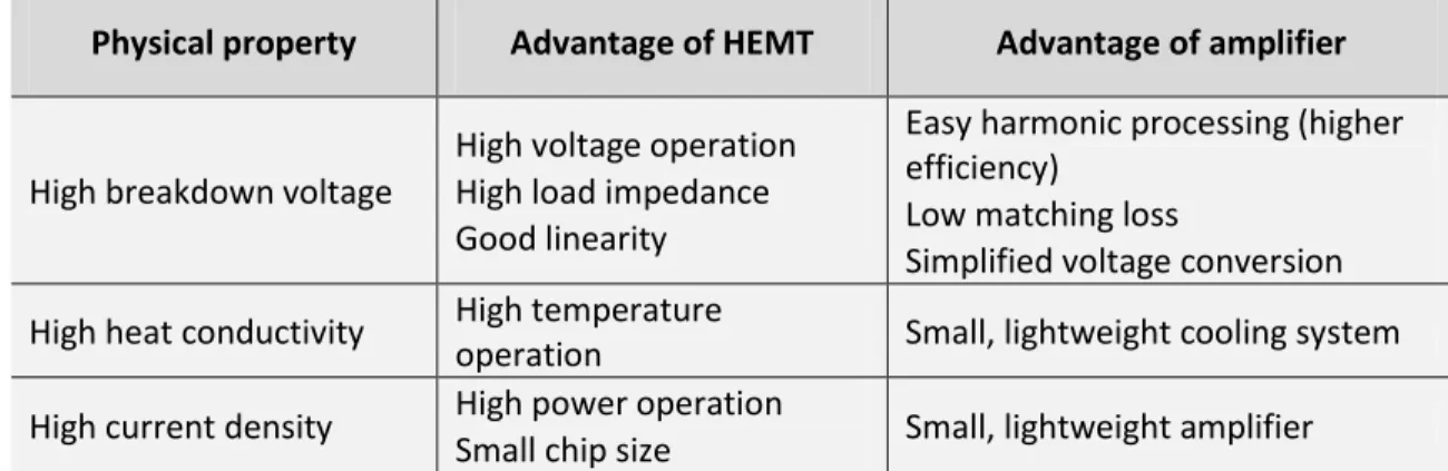
The advantages of GaN HEMT amplifiers are synthesized in Table I-1.
Physical property Advantage of HEMT Advantage of amplifier
High breakdown voltage
High voltage operation
High load impedance
Good linearity
Easy harmonic processing (higher efficiency)
Low matching loss
Simplified voltage conversion
High heat conductivity High temperature
operation Small, lightweight cooling system
High current density High power operation
Small chip size Small, lightweight amplifier Table I-1. Advantages of a GaN HEMT amplifier. [10]
I.3 Wide bandgap semiconductors: electrical parameters
The wide bandgap semiconductors and more specifically the III-N composites like GaN and AlN are excellent candidates for high power and high frequency devices. They present properties for high thermal conductivity, high breakdown field and high velocity of free carriers. These technologies present alternative solutions to meet the needs for the fabrication of high power devices.
Table I-2 resumes the main physical and electrical parameters for different materials. The main parameters qualifying a technology are detailed afterward.
Technology Si GaAs 4H-SiC InP GaN AlN Diamond
Eg (eV) 1.12 1.43 3.26 1.3 3.39 6.2 5.45 ni (cm-3) 1.5×10¹⁰ 1.79×10⁶ 8.2×10⁹ - 1.9×10¹⁰ 1×1031 1.6×1027 εr 11.8 12.5 10 12.5 9 8.4 5.5 µn (cm2V-1.s-1) 1350 8500 750 5400 1500 1100 1900 Ec (106 Vcm-1) 0.3 0.4 3 0.5 3.4 - 5.6 Vsat(.107 cm.s-1) 1 2 2 1 2.5 2 2.7 Tmax (°C) 300 300 600 150 700 - -
Table I-2. Electrical parameters of different technologies used for the fabrication of electronic devices [14] [15] [16].
I.3.1 Bandgap
The bandgap (EG) is the gap between the lower energy of the conduction band (EC) and the higher
energy of the valence band (EV). It is the energy necessary for an electron to reach from EV to EC. The
high power capability of the GaN technology is mainly related to its wide bandgap of 3.4 eV in comparison with Si and GaAs (Table I-2).
9 Where T is the temperature in Kelvin and α and β are constant coefficients equal to 7.7×10⁻⁴ eV.K-1 and 600 K respectively. The bandgap of the AlGaN barrier lowers (as well as the breakdown voltage) of 0.1 eV when the temperature increases from 298K to 523K.
I.3.2 Surface mobility
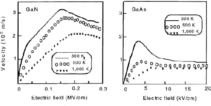
In some words, it is related to the free carrier transportation in the SC, any modification in the crystal lattice causes a change in the mobility. Figure I-4 extracted from [17] compares the calculated temperature dependencies of the electron mobility in bulk GaN and GaAs with and without accounting for the impurity scattering. From this figure, it can be concluded that the electron mobility in bulk GaN is less sensitive to ionized impurity scattering than that in GaAs.
For high frequency applications, a high mobility and high saturation velocity are required. The mobility in the GaN (and SiC) being smaller than that in GaAs, hence this stands as a disadvantage for the fabrication of devices (such as HEMTs) for high mobility applications. However, these values of mobility in GaN are sufficient for transistors specifically designed for high power operation.
Figure I-4. Calculated temperature dependencies of the electron mobility in GaAs and GaN with and without accounting for the impurity scattering [17].
I.3.3 Breakdown voltage
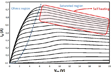
The breakdown of any device is usually caused by impact ionization. Moreover, the measurement of the breakdown voltage for normally-on devices is very difficult due to the high powers that they can resist and to excessive self-heating. Thus, the breakdown voltage measured under normally-off configuration will be the relevant parameter.
10 Figure I-5- extracted from [17] - shows the computed velocity-electrical-field characteristics of GaN and GaAs at different temperatures. It can be concluded that GaN devices are less sensitive to temperature, able to sustain self-heating and suitable for high temperature applications. Hence, from all these characteristics, this figure highlights the ability of GaN versus GaAs for high power and high temperature applications. Considering that Si and GaAs HEMTs represent today’s conventional devices in the market, GaN HEMTs on SiC (Si, also even if less developed but still on the roadmaps for some developers such as Nitronex and Triquint) are expected to be the next generation power devices. Because GaN-HEMTs on Si are still suffering from low breakdown voltages (for example the breakdown voltage of 600V is observed on an HEMT with a 2 µm epitaxial layer on Si substrates, while for the same thickness 1.9 kV has been extracted on a SiC substrate). Some solutions are still under study to improve the device breakdown voltage like increasing the buffer thickness as proposed in [18] where 1.8 kV has been observed or doping the buffer with Fe or C [18]: these parameters are essentially important considering switching applications (switches, class E, F … amplifiers). However, for RF applications, the improvement on the junction temperature (reduction) and on the power added efficiency (PAE increase) represents the real challenges for the GaN technologies.
Figure I-5. Velocity electrical-field characteristics of GaN (a) and GaAs (b) at different temperatures. (a) is after [19]. (b) is computed using the Monte Carlo calculation’s fit reported in
[20] for the following values of the low field mobility: 7000 cm².V-1s-1 at 300K, 3000 cm².V-1s-1 at 500K and 1100 cm².V-1s-1 at 1000K.
I.3.4 Figure of merits for power modules
A figure of merit is necessary to evaluate the potential of a material with the intended application. Several figures of merits exist [39] [40] [41]:
Johnson’s figure of merit (JM) for high frequency devices
(2)
Keye’s figure of merit (KM) when considering thermal limits
11 semiconductors in bold are the best for high frequency and high power applications.
Si GaAs 4H-SiC GaN AlN Diamond
JM 1 7.1 180 760 5120 2540
KM 1 0.45 4.6 1.6 21 32.1
BM 1 15.6 130 650 31700 4110
BHFM 1 10.8 22.9 77.8 1100 470
Table I-3. Normalized figures of merit of important semiconductors for high-voltage power devices. [39] [40] [41]
For high frequency applications, some other figure of merits are more prone to make comparison between technologies, such as the transition frequency ft, the maximum oscillation frequency fmax
and also the power added efficiency PAE for power modules.
I.4 HEMT devices
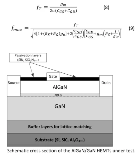
I.4.1 General information
High Electron Mobility Transistors (HEMTs) using AlGaN/GaN heterojunction also known as Modulation-doped FET (MODFET) or Heterojunction FET (HFET), are devices featuring a junction between two different bandgap regions; one undoped (GaN) and the other lightly doped (or also non-intentionally doped, the AlGaN layer). Figure I-6shows a schematic illustration of the transistor.
The transistor can be developed using two techniques: the MetalOrganic Chemical Vapor Deposition (MOCVD) technique and Molecular Beam Epitaxy (MBE) techniques.
As for the fabrication of the device, due to lattice mismatch between GaN and the substrate (Si, SiC, GaN or Al2O3) several layers are added on the Si substrate before introducing the GaN layer.
Table I-4 presents the thermal conductivity and the lattice mismatches between the GaN and many substrates: it can be noticed that a GaN substrate matches the best but the conductivity stands better for a SiC substrate. The very low thermal conductivity of the sapphire substrate prevents it to be used for high power applications although its low cost, hence the Si stand as compromising candidate due to its better thermal conductivity and low cost in comparison with SiC (as well as the possible compatibility with Si technologies for digital command). Etchings in the AlGaN layer are performed for the Ohmic contacts necessary for source and drain terminals. The Schottky contact and the gate access are the first parameters to investigate when studying the gate control and
12 leakage conduction mechanisms. The gate voltage modulates the channel conduction. In this work, normally-on transistors are presented.
Substrate Thermal conductivity (Wcm-1K-1) Lattice mismatch (%)
Si 1.5 17
SiC 4.9 4
GaN 1.7 0
Al2O3 0.5 14
Table I-4. Thermal conductivity and lattice mismatch of different substrates
The characteristics of such devices for high power applications are the maximum drain–source current Imax and the transconductance gain gm given below:
(6)
(7)
as well as the transition frequency (fT) and the maximum oscillation frequency frequencies (fmax):
(8) (9) AlGaN Gate 2DEG Passivation layers (SiN, SiO3N4…)
Buffer layers for lattice matching Substrate (Si, SiC, Al2O3…)
GaN
Source Drain
Figure I-6. Schematic cross section of the AlGaN/GaN HEMTs under test.
Figure I-7 [21] shows the commercialization roadmap of GaN HEMTs for several applications in the different frequency ranges. Since 2005, commercialized power amplifiers for wireless base stations exist. The expectations highlight on wireless mobile networks to move up to 4G mobile technologies and then to go deeper for millimeter wave communications.
13 Figure I-7. Commercialization roadmap of GaN HEMTs for several applications in different
frequency ranges. [21]
I.4.2 GaN versus GaAs and InP power HEMTs
The GaN based devices are the upcoming alternative solution for Si, GaAs and InP based high frequency power HEMTs. Thus, it is of great importance to compare between HEMTs based on these technologies knowing the fact that Si and GaAs-based devices became commercial long time ago, contrarily to GaN and InP HEMTs that are still between laboratory and market products; these latter still suffer of lack of reliability (GaN) or high cost of production (InP, GaN), hence they need more investigations before emerging completely the market.
Based on the results presented in Table I-5:
The high breakdown voltages and excellent thermal conductivities allow a device to behave at high efficiency characteristics at full power. Consequently, the thermal conductivities of GaN are up to 2 W.cm-1K-1 versus 0.46 W.cm-1K-1 for GaAs.
InP HEMTs provide the highest fT and fmax due to high vs so they are only used at high
frequencies due to the high cost of production.
Moreover, due to its wide bandgap, the GaN based HEMTs can reach higher intrinsic temperatures (up to 700°C) and are less sensitive to temperature variations than the GaAs (Tmax=300°C). So, GaN devices can operate with less cooling in complicated structures and are
suitable for high temperature applications more than the GaAs devices.
Device Heterojunction µ (cm²V-1.s-1) K300K (W.cm-1.K-1) Vbr (V) fT (GHz) fmax (GHz)
GaN HEMT Al0.3Ga0.7N/GaN 1180 2 40 65 180
GaAs PHEMT Al0.3Ga0.7S/GaAs 8500 0.46 7 130 250
InP HEMT Al0.5In0.5As/In0.6Ga0.4S 13000 - 5 290 480
14 Moreover, Figure I-8 shows the power and frequency ranges of different technologies and semiconductors present today in the market. It can be seen, that GaN HEMTs reach high powers (≅ 1kW) at high frequencies (≅ 100GHz), contrarily to GaAs and Si-based devices.
Figure I-8. Power versus frequency ranges of different semiconductor materials. [23]
I.4.3 Gate access: Schottky contact and gate current carrier transport
I.4.3.a
Schottky contacts
The carrier transport control is a concern; and for reliable devices, the Schottky and Ohmic contacts must be controlled rigorously and mainly during the fabrication of the device.
The purpose of the Schottky contact is to create a space charge region that modulates the carriers in the channel, and to stand as a barrier that prevents from a high leakage current of the gate. Hence, this contact has an important impact on the reliability and its degradation affects the device operation. Thus, a poor Schottky contact presents high gate leakage current conduction mechanisms. The IG-VGS measurements of a transistor bring information about the leakage level
(IG=0A for ideal conditions). The well-known Schottky barriers are usually made by deposition of
different transition metals such as: Ni/Au, Ni/Ti/Au and Pt/Au. The effects of temperature are a first parameter to consider to metal diffusion, also called “gate sinking”. Several studies showed that slight metal diffusion of the barrier height made with WSiN/Au and Ir/Au was observed at 500°C during a stress of 120 hours whereas Schottky contacts made with Pt/Ni degraded under the same experimental conditions [24] [25] [26].
I.4.3.b
Gate current carrier transport
Several models are proposed in the literature for carrier transport across contacts and interfaces, Padovani and Stratton [27] first evoked on the transport mechanism in 1966 (and most of the papers and models in the literature afterward were based on their considerations). They distinguished three different conduction mechanisms of the gate current: the Thermoionic Emission (TE), the Thermoionic Field Emission (TFE) and the Field Emission (FE) (Figure I-9 and Figure I-10). These three
15 only contribution to the current. At an intermediate temperature range, the electrons tunnel at an energy Em above the conduction band smaller than the energy Eb of the top of the barrier. At higher
temperatures, the TE dominates and the electrons are emitted over the top of the barrier [27]. These emissions are illustrated in Figure I-9.
TE TFE FE dF qV Metal Semiconductor EC EF EV qVn qVb0 qVb IG e EB Em
Figure I-9. Electron potential energy diagram of a forward biased Schottky barrier. TE, TFE and FE present the emission types and the distribution density probability of each
type is shown in the figure. [27]
Reverse current-voltage characteristic
The reverse bias applied to the gate access increases the field in the junction and thus increases the probability for an electron to tunnel from the metal into the semiconductor. Similarly, under reverse conduction mechanisms the FE and TFE are also the dominant parameters. At low temperatures, most of the electrons originate from the Fermi level of the metal. At intermediate temperature range, the conduction occurs between the Fermi level of the metal and the top of the barrier (EB) at an energy level Em. According to Padovani and Stratton [27], under reverse conduction
16 mechanisms, there is no consideration of higher temperatures where the conduction is controlled by reduction of the barrier height by image force correction that is more important under reverse biasing conditions and presented in Eq. 6; the effective barrier height calculated from the traditional current voltage expression will include the image force lowering [28]. Figure I-10 illustrates the electron potential energy diagram of a reverse biased Schottky barrier.
(10)
where E is the electric field at the metal-semiconductor interface and q is the electron charge.
TFE dr qIVI Metal Semiconductor EC EF EV qVn qVb0 qVb e FE qɸb Em qΔɸ qɸb0 EB
Figure I-10. Electron potential energy diagram of a reverse biased Schottky barrier. [27] In the present document, the study is focused on the forward conduction mechanisms and on the reverse conduction mechanisms, even if more attention is given to the exploitation of forward biasing conditions.
The tunneling electrons can accumulate and conduct along the surface of the SC near the gate, creating a virtual gate effect and increasing the gate length. As the tunneling proceeds, an IGD leakage
current is also established between the gate and the drain terminals. The tunneling electrons can go also deeper into the SC (deeper in the AlGaN layer) to reach the 2DEG conducting channel [29], and here the gate access loses the control of the drain current rate in the channel. Solutions are used to reduce the tunneling electrons through the barrier: the reduction of the leakage current can be obtained by adding a field plate (that lowers the maximum voltage into local zones of the device, near the gate edges) as well as by using an efficient passivation layer. A model is presented in the literature to reduce the tunneling leakage current. [30]
Figure I-11 extracted from [29] shows the electron tunneling leakage from the gate electrode and its possible current paths. According to Trew et al. “the electrons that tunnel from the gate electrode
17 Figure I-11. Electron tunneling leakage from the gate electrode and possible current paths.[29]
I.4.4 Drain and source accesses: Ohmic contacts
As for the Ohmic contacts, Ti/Al alloys are usually used for the fabrication of drain and source Ohmic contacts. Since the Aluminium presents risks for cracks and oxidations, other alloys of transition metals are also studied such as Ti/Au, Ni/Au, Pt/Au, Ir/Au and Nb/Au for more robust Ohmic contacts. Some contacts made by deposition of Ti/WSiN/Au has shown stability at 800°C for 20 minutes and classic contacts such as Ti/Al/Ni/Au with WSiN barrier has shown stability at 500°C for 120 hours. [24] [26]
The drain current carrier transport is also important to be controlled at the drain and source Ohmic contacts that govern the drain current. Moreover, the interface AlGaN/GaN where the carrier flows is also a concern and the roughness of this interface and the dislocations generated from the substrate may create trapping/detrapping effects. The contact resistors of the source (RS) and the
drain (RD) accesses may reduce the current and hence the power in the channel. In the Ohmic region,
the drain current is linear versus VDS following the well know Ohm’s law with a resistance equivalent
to the sum of the drain and source resistors, as well as the channel resistance (Req=RD+RS+RCh). The
saturation of the current appears between 5 and 10 kVcm-1.
I.5 GaN technology: a matter of electro-mechanico-thermal
management
I.5.1 Piezoelectric and spontaneous polarizations
I.5.1.a
Piezoelectric polarization
The GaN technology and all other III-N nitrides such as AlN and InN suffer of large piezoelectrical and spontaneous polarization effects at heterointerfaces [22], under the gate in the AlGaN layer and also in the GaN buffer layer. The piezoelectric effects appear when the layer is submitted to stresses that change the symmetric characteristic of the crystal (due to mechanical stresses).
18 The generation of piezoelectric strain can lead to the creation of defects that can act as traps for electron transport. GaN and AlN show strongly pronounced piezoelectric effects and because of the Wurtzite properties of GaN and AlGaN structures, the crystal growth is in the c-axis direction, all these considerations affect directly the electric field in the direction perpendicular to the AlGaN/GaN heterointerface. According to Ambacher et al. [31] in Wurtzite structure AlGaN/GaN HEMTs, the piezoelectric polarization of the strained top layer is more than five times larger as compared to AlGaAs/GaAs structures. This may lead to a significant increase of the sheet carrier concentration at the interface. The increase of charges can generate trapping-detrapping processes and lag effects in the device. The piezoelectric polarization in the AlxGa1-xN is given by:
(11)
where εGaN and εAlGaN are the dielectric constants, and FGaN and FAlGaN are the interface values of the
electric field in GaN and AlGaN layers respectively and PAlGaN is the piezoelectric polarization in the
AlGaN layer. In Wurtzite structures, PAlGaN can be expresses in terms of the AlGaN piezoelectric
coefficients e31 and e33 given by:
(12)
where c31 and c33 are the AlGaN elastic constants and uxx is the strain component in the interface
plane. If the dislocations do not relax the strain, then the strain component is given by:
(13)
For an AlGaN/GaN heterojunction, the non-linear dependence of the piezoelectric polarization on the alloy can be approximated by the following quadratic equation [32]:
(14)
I.5.1.b
Spontaneous polarization
Due to the Wurtzite structure along which epitaxial films and AlGaN/GaN heterostructures are grown, the spontaneous polarization is in the c-axis of the crystal following the equation:
(15)
They mainly exist in the GaN layer where the effect is generated from the nitride to the gallium, noted Psp and given by the Aluminium concentration as follows:
(16)
It is noticed that the Psp in the GaN layer is equal to -0.029 C/m².
The spontaneous polarization is independent of the electric field and of the stress, and it is due to the polar bond between the gallium and the nitride. When the non-ideality of the structure increases the spontaneous polarization increases.
19
AlN GaN InN
e31 (Cm-²) -0.58 -0.49 -0.57
e33 (Cm-²) 1.55 0.73 0.97
Table I-6. Pizoelectrical and spontaneous polarization constant for different III-N technologies [33].
-+ + + + + + + + + + + + + + + + + + + + + + + +
Al
xGa
1-xN
GaN
[0001]
P
SPP
PZP
SP 2DEG σ-surface σ+interface σ2DFigure I-12. Example of Piezoelectrical and spontaneous polarization in the AlGaN and the GaN layers (N ended).
Equations (18), (19) and (20) show the relation between the piezoelectric and spontaneous polarizations with the threshold voltage, the carrier density and the drain current respectively:
(18)
(19) (20)
where P1 and P2 are the strain tensors, C1 and C2 are the elastic constants and d is the thickness of
the layer [28]. Moreover, these polarizations could also affect the sheet resistance of the AlGaN and GaN layers. Equation (21) shows the relation between the mobility (affected by the carrier density) and the sheet resistance:
(21)
where e is the electron mobility, Wch is the thickness of the active channel and Wd is the thickness of
20 density in the channel (as it depends on Vth) and the subsequent drain value IDS. Taking into account
these effects for evaluating the evolutions of the IDS-VGS or gm-VGS plots is then necessary.
I.5.2 Thermal management
The operating channel temperature is one of the main device reliability indicators for AlGaN/GaN HEMTs. Therefore, it is of great importance to determine the channel conductivity and the maximum operating temperature for transistors dissipating large amount of thermal energy [34].
The channel temperature of a device is modeled by its thermal resistance for packaged transistors. Prejs et al. [34] developed a dual-mannered model for thermal resistance determination by using of Infrared microscopy and finite element analysis from which θjc (junction to case thermal
resistance) can be calculated using the following equation:
(22)
And in its simplest form can be presented as the sum of a series of component resistance as shown below:
(23)
Using these values in a casual way to determine thermal resistance in scenarios other than how they were measured will lead to erroneous results [34]. Moreover, according to the complexity of the packaging and die design (multifinger power die), the model of the thermal resistance can be much more complex since every element in the system is contributing to the overall heat flow (multi stage serial resistors cells). The conventional thermal management technique is presented in Figure I-13 extracted from [35] and shows the main elements that contribute to the heat flow. According to Laskar et al. [35] the heat spreads from the device channel, vertically through the layers.
Figure I-13. Conventional and flip-chip representations of the channel temperature. [35] In a conventional configuration the channel temperature can be approximated by [35]:
(24)
And, in a flip-chip configuration, it can be approximated by [35]:
21 a lot of parameters impact the transistor channel temperature such as the substrate thickness, as well as the device geometrical parameters (number of fingers, gate pitch…) and the PAE in circuit design because it controls the total power to dissipate in the device when designing the power amplifiers (PA).
Figure I-14 shows the channel temperature versus the power density of 3 different HEMTs (GaAs on Si, GaN on Si and GaN on SiC). It is noticeable that GaN on SiC HEMTs provide the best channel temperature even at high power densities in comparison with GaAs on Si and GaN on Si HEMTs.
Figure I-14. Channel temperature versus power density of three different HEMTs: GaAs on Si (in black), GaN on Si (in red) and GaN on SiC (in green). [36]
I.6 Stresses
I.6.1 Arrhenius accelerated lifetime testing
Since a product lifetime is very long under normal operating conditions, therefore it is of great interest to develop accelerated life tests. Under these conditions, an artificial stress can be performed on devices that accelerate their time to failure. Arrhenius reported in 1887 about a lifetime testing based on Eq. 26 [29]:
(26)
where R is the reaction rate, T is the temperature, A is a constant, Ea is an activation energy and k is
22 the reaction rate. Each life test yield to a failure rate λ as expressed in Eq. 27 showing the relationship between failure rate and the Khi2 distribution:
(27)
where TDH is the “Total Device Hours” of the test and AF is an acceleration factor, both of them can be expressed as follows:
(28)
and
(29)
where N is the number of units being tested, H is the hours they are subjected to the test, Top is the
operating temperature and Tstress is the elevated stress temperature used in the accelerated life test.
The lifetime of a device is determined as a function of the stress parameter (temperature). Each activation energy is the parameter that provides the information on each failure mechanism on the device by solving a sequence of equation-tests performed at two different temperatures following these equations:
For the first temperature T1:
(30)
For the second temperature T2:
(31)
The activation energy can be written as:
(32)
where tf1 and tf2 are the time to failure at T1 and T2 corresponding temperatures respectively [7]. This
is valuable if considering a single failure with activation energy Ea. Then the temperature range of the
study (and then the time to degradation) must be chosen to evidence realistic failure modes for a given set of applications (other techniques can be used, as proposed in the next chapter, to extract activation energies). Indeed, at least 3 temperatures are needed to assess for the accelerated dependence of the degradation (to reveal the linear trend related to the mathematical expression), and to extract the related activation energy. Moreover, the temperature range should not be too much elevated, as different activation energies can be evidenced in comparison with the activation energy that should be revealed by the investigation at lower temperatures (in spite of a longer time until the degradation occurs).
I.6.2 DC stresses
For lifetime testing, other types of stresses may be also applied such as the DC stresses. They are also temperature dependent stresses where the resultant parameter is also activation energy. We distinguish three types of DC stresses usually used for lifetime testing.
23 low enough to be considered as null). This stress intends to validate the robustness of the Schottky contact under high electric field. The biasing conditions are: VDS=50V, VGS=-7V (deeply pinched off) at
175°C. If after several hours (usually 2000 hours) no drift of the Schottky contact and of the DC parameters of the device are reported, then the test is considered as successful [37].
I.6.2.b
High Temperature Operating Life (HTOL) stress
This stress is performed at room temperature and the thermal stresses are exhibited through high drain-to-source voltages (VDS) at VGS=0V (open channel). The junction temperature varies
following the current rate in the channel. During this stress, the DC and RF characterizations are performed after 48h, 96h, 192h, 450h, 1000h, 2000h, 3000h, etc. The failure mechanism is related to the drain current run-away which consists in a loss of the drain current control as illustrated in Figure I-15 (extracted from [37]).
Figure I-15.Output characteristics measured by means of a curve tracer at different temperatures for a device exhibiting a runaway mechanism (ellipse area). [37]
I.6.2.c
IDQ stress
This stress is also applied at room temperature at constant IDS with an average value of VDS where
the gate-to-source voltage (VGS) is dependent of the drain current needed to apply the stress. The
result is an average junction temperature. Less degradation can be observed within the IDQ stress in comparison with HTRB and HTOL stresses.
24 Table I-7 - extracted from [37] - presents an example of qualification test plan of UMS (our manufacturer) that consists of a set of ageing tests and it covers environmental tests, Safe Operating Area definition, including recommended Operating Rating (OR) and Absolute Maximum Rating (AMR) as well as the assessment of wear-out mechanisms [37].
Test DUT Conditions Test type Duration
Storage Wafer 250, 300°C Diffusion 2000 h
TC RIC -65, +125°C CTE 500 cycles
THB RIC 85°C, 85% Humidity 1000 h
DCSST DEC 50V + n × 5V AMR 1st failure
RFSST DEC 50V + n × 5V, PAEmax+N × 1 dBm
AMR 1st failure
HTRB DEC 100V, -7V, 175°C Schottky 2000 h
HTOL DEC 50V, 3 temp Wear out 70% failure
DCLT-1 DEC 50V, 250°C MTTF >2000 h
DCLT-2 RIC 50V, 200°C MTTF 2000 h
RFLT-1 DEC 50V, PAEmax MTTF 2000 h
RFLT-2 RIC 50V, PAEmax MTTF 1000 h
VSWR RIC 50V, |3|,|5|,|10| Robustness All phases
Table I-7. GH50-10 qualification test plan. [37]
I.6.2.d
Step stress
The step stress is a non-thermal stress (performed at room temperature) where the parameters inducing the stress are the voltage, current or RF power variations. The purpose of this stress is to identify the Absolute Maximum Rating (AMR) [37]. This type of stress can be performed monotonically with a recovery time. Figure I-16 extracted from [38] shows examples of devices degrading rapidly or gradually during step-stressing action. An example of step stress test is proposed in Figure I-17 from [37] by our manufacturer UMS [8], on a devices stepping the compression level as PAEmax, PAEmax+1 dBm and PAEmax+2 dBm. After each compression cycle, VDS is
increased by a step of 5V starting from 50V. Failures occurred at the step VDS=60V and PAEmax+2 dBm
(as shown in Figure I-17). Hence, the AMR of this technology is fixed today at VDS=60V and PAEmax+1
dBm. Nevertheless failures occurred for conditions where the device was not sufficiently matched, and they are attributed to an excessive induced junction temperature [37].
Figure I-16. Examples of typical time dependence of stressing protocols [38] (stresses performed to control jamming (electronic warfare) or radar overshooting).
25 Figure I-17. RF gain monitored during RFSST test. Pin is set such as the device was operating at
the maximum PAE, PAEmax+1 dBm and PAEmax+2 dBm. Starting from VDS=50V, after each
compression cycle, the VDS is step up by 5V. [37]
I.7 Reliability of GaN devices
In the first stages of GaN reliability studies, researches have been driven using the same procedures and roadmaps for GaAs technologies. However, till the middle of 2005, lots of peculiar degradation behavior could not be interpreted using established theories. Then, GaN technologies have been considered in a much more realistic context considering all the potential effects and their interactions. But everything was to be developed (experimental tools for destructive and non-destructive analysis to be matched, theories to be gathered, etc.). This stands as the starting point for the ReAGaN project, involving different partners with specific expertise in the many areas of interest.
We distinguish two types of failures: Catastrophic (destructive or permanent degradation) and recoverable degradation.
Moreover, the Mean Time To Failure (MTTF) in any device is important reliability indicator. It is carried out on n devices that fail at several operating times tn. The Mean Time To Failure is given by
Eq. 34 [42]:
(34)
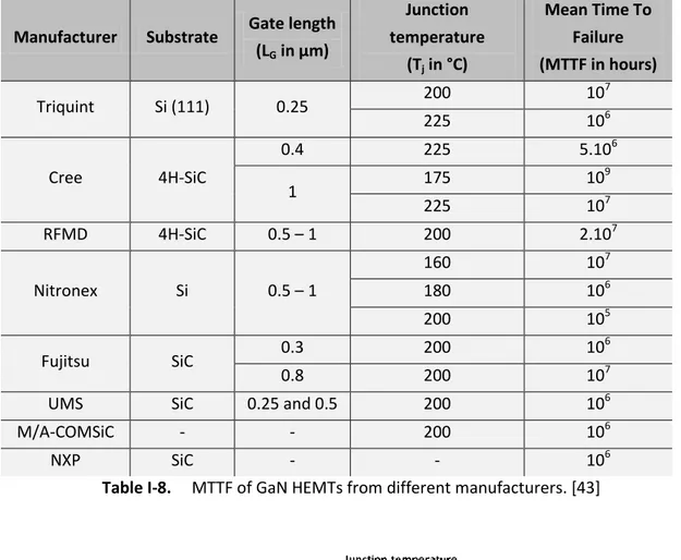
The experimental techniques to determine the MTTF are more rigorous and give accurate information rather than the theoretical techniques. Great values of 107h of MTTF have been reported at junction temperature below 200°C, with activation energies ranging from 0.18 to 2 eV, but without taking into account the high electric field and current when determining the device lifetime. Table I-8 [43] synthesizes the MTTF of GaN HEMTs from different manufacturers. As for our manufacturer (UMS), Figure I-18 (extracted from [37]) shows the Arrhenius plot of devices submitted to an HTOL stress test. A MTTF of 3×10⁷ hours is observed for a junction temperature of 175°C with associated
![Figure I-4. Calculated temperature dependencies of the electron mobility in GaAs and GaN with and without accounting for the impurity scattering [17].](https://thumb-eu.123doks.com/thumbv2/123doknet/2218534.14631/21.893.198.736.719.922/calculated-temperature-dependencies-electron-mobility-accounting-impurity-scattering.webp)

![Figure II-16. Example of GaN HEMT LFN spectrum featuring the contributing noise sources [10]](https://thumb-eu.123doks.com/thumbv2/123doknet/2218534.14631/71.893.166.732.374.675/figure-example-hemt-spectrum-featuring-contributing-noise-sources.webp)