HAL Id: hal-03052881
https://hal.archives-ouvertes.fr/hal-03052881
Submitted on 10 Dec 2020HAL is a multi-disciplinary open access archive for the deposit and dissemination of sci-entific research documents, whether they are pub-lished or not. The documents may come from teaching and research institutions in France or abroad, or from public or private research centers.
L’archive ouverte pluridisciplinaire HAL, est destinée au dépôt et à la diffusion de documents scientifiques de niveau recherche, publiés ou non, émanant des établissements d’enseignement et de recherche français ou étrangers, des laboratoires publics ou privés.
Porosity calibration in a 4-layer porous silicon structure
to fabricate a micro-resonator with well-defined
refractive indices and dedicated to biosensing
applications
Fabien Cassio, Nathalie Lorrain, Parastesh Pirasteh, Luiz Poffo, Jonathan
Lemaitre, Isabelle Hardy, Mohammed Guendouz
To cite this version:
Fabien Cassio, Nathalie Lorrain, Parastesh Pirasteh, Luiz Poffo, Jonathan Lemaitre, et al.. Poros-ity calibration in a 4-layer porous silicon structure to fabricate a micro-resonator with well-defined refractive indices and dedicated to biosensing applications. Optical Materials, Elsevier, 2020, 110, pp.110468. �10.1016/j.optmat.2020.110468�. �hal-03052881�
1
Porosity calibration in a 4-layer porous silicon structure to fabricate a
micro-resonator with well-defined refractive indices and dedicated to
biosensing applications
F. Cassio1, N. Lorrain1*, P. Pirasteh1, L. Poffo1,J. Lemaitre1, I. Hardy1,2 and M. Guendouz1
1
Université de Rennes 1, Institut Foton- UMR 6082, F22305, Lannion, France
2
IMT Atlantique, Institut Foton- UMR 6082, F29238, Brest, France *Corresponding author: nathalie.lorrain@univ-rennes1.fr
Abstract
Calibration of the porosity as well as the electrochemical anodization rate in a 4-layer porous silicon (PSi) waveguide structure, including a guiding, a confinement and two technological barrier layers, is studied and validated. The objective is to process using standard photolithography a 4-layer PSi micro-resonator (MR) that will be butt coupled with polymer waveguide and used for biosensing applications. The knowledge of the porosity and thus the refractive index of each PSi layer is then crucial to fabricate the hybrid optical component. The presence of the two PSi barrier layers is necessary to prevent the infiltration of polymers or resin during the process but influences the porosity and the anodization rate of both the guiding and the confinement PSi layers. Their porosity is lower than if these layers had been manufactured separately (one layer only) and the anodization rate is on the contrary higher. Taking into consideration the calibration results to obtain the target thicknesses and refractive indices of the guiding and the confinement PSi layers respectively, a MR based on the 4-layer PSi structure is fabricated. The PSi MR experimental transmission spectrum well corresponds to the simulated one which has been calculated from porosity calibration results and from experimental dimensions of the component measured by scanning electron microscope observations. Finally, a promising theoretical surface sensitivity of 0.06 nm/(pg/mm²) for Bovin Serum Albumin detection with a limit of detection of 0.1 pg/mm² has been calculated for the PSi MR.
Keywords: Porous silicon, multilayers, porosity calibration, micro-resonator.
1. Introduction
Porous silicon (PSi) is a widely studied material that is used in many applications, particularly in the field of label free biosensors due to its large surface specific area and its biocompatibility [1]. In addition, the adequate functionalization of the surface of the internal pores introduces the ability to specifically detect molecules of interest, which is necessary for early diagnosis of diseases. Due to the electrochemical anodization used process, the porosity and the thickness of the PSi layers are tunable, making it possible to manufacture many components that have been used for biosensing applications [2 - 4]. Thus, double-layer structures for waveguides [5], interferometers [6, 7], optical grating [8], micro-resonators [9,
2
10] and photonic crystals [11], or multi-layer structures for Bragg mirror [12, 13], micro-cavities [14, 15] and rugate filters [16] have been fabricated for biosensing applications in integrated optic.
In the field of integrated optic, micro-resonators (MRs) are certainly the smallest structures to obtain very sensitive sensors with low limit of detection compared to interferometers for example [17]. Most MRs are geared toward classical detection based on refractive index variations where the probed molecules interact with the evanescent wave [17, 18]. MRs biosensors based on PSi technology offer an enhancement of the sensitivity, and so an improvement of the limit of detection compared to bulk MR biosensors, due to a direct interaction of specific biomolecules grafted on the internal surface of pores and the propagated light [19, 20], [11].
Waveguides made in PSi have higher optical losses than those made in a bulk material due to their porous nature. In order to reduce the losses in the whole optical biosensor, we planned to implement a hybrid structure by associating the PSi transducer MR with polymer waveguides that will ensure the transmission and recovery of the optical signal with lower optical losses [21, 22]. For this aim, the PSi MR will be butt-coupled to the polymer waveguides with the constraint that the refractive index of the PSi guiding layer corresponds to that of the polymer core waveguide. Moreover, to further fabricate this hybrid structure, a 4-layer PSi structure will be needed since guiding and confinement PSi layers will be subjected to a photolithography process inducing a resin deposit and then a polymer deposit. Consequently, both the guiding and the confinement layers have to be protected by a thin PSi barrier layers of low porosity to prevent from polymer or resin infiltration.
In PSi multilayer structures, the porosity and thus the refractive index of the guiding and confinement layers are often deduced from a calibration based on the elaboration and characterization of a single layer by assuming, as a first approximation, that the porosity of a single layer is the same than in a multilayer structure for the same fabrication parameters [5, 23-26]. However, some authors mentioned that the so-determined refractive indices and also the anodization rate of PSi layers are modified in presence of a multilayer structure [27]. It was reported that the measured refractive indices and anodization rates were systematically lower for thin and extremely high porous layers in presence of a PSi multilayer structure compared to a thick layer one [28, 29].
In this paper, a calibration of the porosity and the anodization rate of the guiding and confinement PSi layers is performed taking into consideration the presence of the thin PSi technological barrier layers. The objective is to define the current densities and anodization times that must be applied to obtain guiding and confinement PSi layers with well-defined refractive indices and thicknesses to be able to manufacture a 4-layer PSi MR. We first present the technological steps to fabricate the MR based on 4-layer PSi ridge waveguides. Then we present the method we have used to determine the porosity and thus the refractive index of each layer. The calibration results are presented and discussed. The 4-PSi layer MR is fabricated and characterized using scanning electron microscope observations and using an optical bench to measure its optical transmission spectrum. Simulations results are presented and compared to the experimental optical characterizations. Finally, as the MR will be used for biosensing applications, a preliminary theoretical study of the surface sensitivity and the limit of detection of the PSi MR for Bovin Serum Albumin (BSA) is presented.
3 2. Experimental
To fabricate a PSi MR that will be butt coupled with SU8 polymer waveguide, four PSi layers are needed since guiding and confinement PSi layers will be subjected to a photolithography process inducing a resin deposit and then SU8 deposit.
The refractive index of the SU8 polymer core waveguide is 1.57 at 1.55 µm. The refractive index at 1.55 µm of the porous confinement of both PSi and SU8 polymer core waveguides has been chosen to 1.41 in relation to a previous work [21]. The target thickness of the confinement layer is about 5 µm. The target dimensions of the ridge core waveguide are a width of 2 µm and a height of 1.7 µm to obtain a single-mode propagation for the TM polarization.
The figure 1.a shows the four consecutive layers of porous silicon prepared by electrochemical anodization of a heavily doped P (100) silicon substrate with a 5 m.cm resistivity and using successive applied current densities for specific times. The electrolyte is a mixture of hydrofluoric acid (50 %) with ethanol and deionized water in the ratio of 2-2-1 respectively. The room temperature is maintained at 18 °C. The first and the third thin barrier layers with low porosities are obtained with a current density of 1 mA/cm². The target thicknesses of the four layers are respectively of 30 nm, 1.7 µm, 50 nm and 5 µm. In the waveguide structure, the first and the third layers do not exceed 50 nm to ensure single-mode waveguide @ 1550 nm.
To obtain the 4-layer PSi MR, a thin SiO2 layer of about 30 nm is deposited on the first PSi
barrier layer to further improve the impermeability of the porous structure. We have found that this thin SiO2 layer directly deposited on the guiding PSi layer do not ensure the role of
technological barrier to prevent from infiltration of resin in pores. Then, a positive S1805 photosensitive resin layer is deposited by spin coating on the technological barriers (SiO2
layer and first PSi layer). Ridge waveguide patterns are then produced under UV exposure through a well-defined chrome mask designed using commercial Olympios software. The sample is immersed in the MF-319 to reveal the ridge PSi waveguide patterns.
A trifluoromethane (CHF3) Inductively Coupled Plasma (ICP) is performed in order to etch
the first technological barrier layers and the guiding layer. The etching depth should be controlled to avoid the etching of the second PSi barrier layer. The photosensitive resin and the SiO2 layers are then removed respectively with an oxygen (O2) followed by a sulfur
hexafluoride (SF6) Reactive Ion Etching (RIE). The 4-layer PSi MR is then achieved as
4
Figure 1: (a) Schematic representation of the four PSi layers. (b) Schematic representation of the 4-layer PSi MR after a standard photolithographic process.
3. Porosity determination method
In a PSi multilayer structure, it is reported by some authors that the refractive index and the etching rate of a PSi layer are modified compared to a single PSi layer [27]. In a first approximation, the porosity of a layer in a multilayer structure is generally considered identical to that determined on a single layer. This was particularly the case in our previous studies with a good agreement between simulation and experimental results [14, 30] without any use of a technological PSi barrier of low porosity. In our 4-layer PSi structure, we must consider that the refractive index of the guiding and the confinement PSi layers may be affected by the PSi technological barrier layers.
To obtain refractive indices of the PSi guiding and confinement layers of 1.57 and 1.41 respectively, porosities of 69.6% and 76.3% are required. The current densities to be applied to produce these layers with well-defined porosities must be determined by a calibration taking into account the presence of the thin barrier layers.
We consider that changing the current density to perform another PSi layer does not affect the characteristics of the PSi layer previously formed because silicon dissolution occurs at the silicon electrolyte interface [31]. But we assume according to literature [28-29] that the porosity of a layer inside a multilayer structure is not the same as in a single layer.
In case of one single PSi layer (without any technological barrier layer) (figure 3.a), the porosity and so the refractive index are determined by a well-established methodology using reflectance measurements and the Bruggeman model [14, 32-35]. Reflectivity spectrum of the Air/PSi layer/Si substrate interference system is measured in the range 900 – 2000 nm using an Ocean Optics HR 400 spectrometer. The method consists in fitting on the experimental spectrum a theoretical spectrum calculated rigorously using a transfer matrix method [34]. The transfer matrix method allows the reflectivity of the layers to be calculated from data including refractive index and layer thickness. The thickness of the PSi layer is determined by scanning electron microscopy (SEM). The refractive index of the layer is calculated using the approximation of Bruggeman [35].
This method is commonly used in porous silicon [36] and can be applied in our case as the pores dimensions of 20 -40 nm are smaller than the optical wavelength so that the medium behaves homogeneously. This is an effective model that allows to take into account the different medium constituents and their volume fraction. Applied to a PSi layer, the Bruggeman model relates the porosity P and the refractive indices of air, silicon nSi and n, the
effective index of the PSi layer according to following equation (1):
Thus, for a PSi layer, the refractive index dispersion curve is obtained by knowing its porosity. By this method, the theoretical reflectance spectrum is compared to the experimental spectrum of the sample. The calculations are continued, by varying the porosity of the layers, until the two experimental and theoretical curves are fitted. The porosity value of the single PSi layer is then deduced from the best fit between the theoretical and experimental reflectance spectra. An example of an experimental and the adjusted theoretical spectra are reported in figure 2.a for a single layer; the thickness of the layer is obtained from the SEM
5
cross section measurements (figure 2. b) with an accuracy of 0.05 µm. The determined porosity of the PSi layer is 71.1 0.6 % for an applied anodization current density of 80 mA/cm². Moreover, we have verified that the porosity of a 4.75 µm thick-layer is the same as that of a 1.7 µm thick-layer. The porosity of one single layer has been also determined using this method for current densities of 1 mA/cm² corresponding to the PSi barrier layers and in the range of 50 to 110 mA/cm² corresponding to the guiding and the confinement PSi layers respectively.
Figure 2: Example of adjustment of the experimental and calculated spectra (a) for the as prepared porous silicon layer (b).
In order to determine the porosities of the guiding and the confinement PSi layers in a 2 or 4-layer PSi structure, we used the following method described in figures 3.b and 3.c which consists in reducing the study to a single-layer.
Precisely, in order to determine the porosity of the guiding layer which follows the first thin barrier layer, a 2-layer structure is prepared by applying J1 = 1 mA/cm² for the barrier layer
and another one for the guiding layer by applying a current density J2 in the range of 50 to 110
mA/cm². Then, a SF6 RIE etching is performed on the sample to remove the thin barrier layer
(figure 3.b).
In the same way, to determine the porosity of the confinement layer, a 4-layer structure is performed by electrochemical anodization: current densities of J1 = 1 mA/cm², J2 = 85
mA/cm², J3 = 1 mA/cm² and J4 = 110 to 120 mA/cm² are applied successively.
In addition, in order to better identify the second 50 nm barrier layer both in the SEM images and in the RIE etch tracking, a larger thickness of about 300 nm was chosen for the calibration of the porosity of the confinement layer in the 4-layer structure. Then, a SF6 RIE
etching is performed on the sample to remove the three top layers: the two thin barrier layers and the guiding layer (figure 3.c).
6
Figure 3: (a) Study of the porosity of a single PSi layer: schema of the PSi layer corresponding to the guiding layer and prepared by electrochemical anodization by applying a current density J in the range of 50 to 110 mA/cm². (b) Study of the porosity of the guiding layer: schema of a 2-layer structure with the barrier layer in the top and the guiding layer prepared by electrochemical anodization by applying successively the current densities of J1
= 1 mA/cm² and J2 in the range of 50 to 110 mA/cm². Then a SF6 RIE etching is performed to
remove the first thin barrier layer. (c) Study of the porosity of the confinement layer: schema of a 4-layer structure with the barrier layer in the top, the guiding layer, the second barrier layer and the confinement layer prepared by electrochemical anodization by applying successively the current densities of J1 = 1 mA/cm², J2 = 85 mA/cm², J3 = 1 mA/cm² and J4 in
the range of 110 to 120 mA/cm². Then a SF6 RIE etching is performed to remove the three top
7 4. Results and discussions
4.1 Porosity and anodization rate calibrations
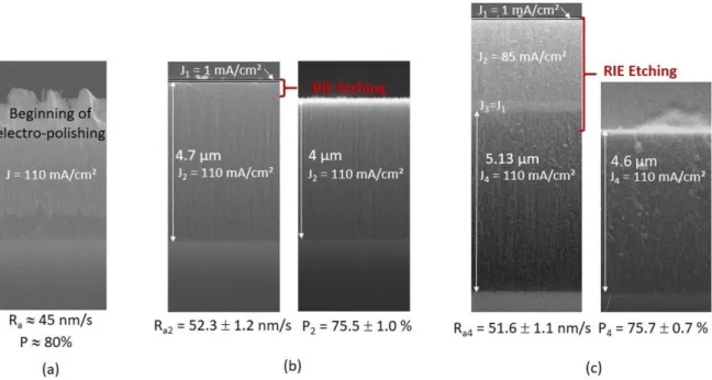
The objective is to determine the porosity (P) and also the electrochemical anodization rate (Ra) of a single layer obtained either just after anodization, or after etching of a 2-layer or a 4-layer structure using the method described in part 3 and to compare them. As an example, the results that have been obtained for the current density of 110 mA/cm² are reported in figure 4 with, in addition, the SEM cross-section observations that have been performed either just after electrochemical anodization (figures 4.a, b or c) or after etching of the tops of the layers to keep only one single layer in case of the 2-layer (figure 4.b) or the 4-layer (figure 4.c) PSi structure.
Figure 4: SEM cross section micrographs of the PSi layers, anodization rate Ra, porosities P estimated by reflectometry adjustment method in a single layer for an applied current density of 110mA/cm²: (a) in one single layer (b) in a 2-layer PSi structure constituted by the barrier layer (J1 = 1mA/cm²) and the studied guiding layer (J2 = 110 mA/cm²) before and after RIE
etching to reduce the structure to a single-layer study to determine the porosity P2. (c) in a
4-layer PSi structure constituted by the barrier 4-layer (J1 = 1 mA/cm²), a second layer J2 = 85
mA/cm², another barrier layer (J3 = J1 = 1 mA/cm²) and the confinement studied layer (J4 =
110 mA/cm²) before and after RIE etching to reduce the structure to a single-layer study to determine the porosity P4.
In figure 4.a, a beginning of electropolishing of the single PSi layer has been observed. Nevertheless, the porosity P and the anodization rate Ra have been estimated around 80 % around 45 nm/s respectively in a non-electro-polished area. In presence of an upper PSi barrier layer, electro-polishing has not been observed: the 2-layer (figure 4.b) and the 4-layer (figure 4.c) PSi structures are undamaged.
In the 2-layer PSi structure (figure 4.b), after a RIE etching of the barrier layer and a part (about 500 nm) of the second layer performed with a current density of J2 =110 mA/cm², the
8
to the uncertainty on thickness and related to the roughness created during the RIE etching step. The anodization rate of the second layer for J2 = 110 mA/cm² is Ra2 = 52.3 1.2 nm/s
when a first layer with a current density of 1 mA/cm² is performed.
Figure 4.c reports a 4-layer PSi structure that represents the multilayer structure that is needed to fabricate the micro-resonator, except for the second barrier layer which is thicker in this case for SEM observations and RIE etching tracking. Apart from the first barrier layer which is very thin and not visible on the SEM image, the other three PSi layers are well defined: the guiding layer corresponding to a current density of 85 mA/cm², the second barrier layer of 280 nm and the confinement layer corresponding to a current density of 110 mA/cm². The RIE etching of the three top layers reducing the structure only to the confinement layer to be characterized, provided the determination of a porosity P4 of 75.7 0.7 %. This porosity P4 is
very similar to the porosity P2 determined in the case presented in figure 4.b for the same
current density of 110 mA/cm². The anodization rate of this confinement layer is Ra4 = 51.6
1.1 nm/s which is also similar to the Ra2 in the case of figure 4.b as the layer just above it is
also a barrier layer performed with the same low current density of 1 mA/cm².
These first results confirm that in a PSi multilayer system, there is an influence of the previous formed low porous layer on the anodization rate and on the porosity of the following layer. Indeed, the porosity of the PSi single layer performed with a current density of 110 mA/cm² is higher than that performed with the presence of a thin top PSi barrier. The porosity and the anodization rate of the layer seem to only depend on the structural characteristics of the previously formed PSi layer because the porosity and the anodization rate are very similar in the cases of figures 4.b and 4.c for which the layer just above the studied one is a barrier layer performed with the current density of 1 mA/cm².
Taking into account these results, the influence of the presence of a thin top barrier layer on the anodization rate and the porosity of the considered PSi layer has been studied for other current densities over 50 mA/cm² and up to electro-polishing. Figure 5 compares anodization rate (figure 5.a) and porosity (figure 5.b) plotted as a function of the current density of the studied layer for three cases. In case A, the studied structure is a single PSi layer manufactured with a current density in the range of 50-100 mA/cm², without any barrier layer. Case B represents a 2-layer PSi structure constituted of the thin barrier and the studied guiding PSi layer performed with a current density in the range of 50-110 mA/cm². Case C concerns the 4-layer PSi waveguide structure constituted of the first barrier layer, the guiding layer prepared with a current density of 85 mA/cm², another thin PSi barrier and the studied confinement PSi layer prepared with a current density in the range of 110-120 mA/cm². Figure 5.a shows that for a current density of 50 mA/cm², the anodization rate is substantially the same for the cases A and B. Then, the difference in anodization rate between the two cases A and B increases even more with the current density applied. A previously formed barrier layer increases the anodization rate of the porous layer under study.
As already observed in figure 4.a, electropolishing phenomenon occurs on a single layer using current densities up to 110 mA/cm² (case A). It is not observed for the layer performed with the same current density of 110 mA/cm² in a 2-layer PSi structure (case B) or in a 4-layer PSi structure (case C) for which electropolishing occurs for higher current densities up to 120 mA/cm².
9
Figure 5: PSi layer (a) anodization rate, (b) porosity and (c) corresponding refractive index versus anodization current density J, (A) : for the case of one single layer; (B): for the case of the 2–layer structure with a barrier layer performed with 1 mA/cm² and the guiding layer with varying current densities in the range of 50-110 mA/cm²; (C): for the case of the 4–layer structure with a barrier layer performed with 1 mA/cm², the guiding layer performed with a current density of 85 mA/cm², a second barrier layer of 1 mA/cm² and the confinement layer performed with a current density of 110 or 115 mA/cm² (for J4 = 120 mA/cm²:
electropolishing).
The porosity calibration curve presented in figure 5.b also shows that the porosity is almost similar for a current density of 50 mA/cm² for the cases A and B. But for increasing current densities and in contrast to the anodization rate, porosity gets higher in the single layer (case A) than in the studied layer in cases B or C. The closer the porosity of the studied and the barrier layers are to each other, the more negligible the influence of the previously formed layer, as shown in figure 5.b. The diffusion of the reactive species responsible for pore formation is all the more limited through the barrier as its porosity is low. The composition of the electrolyte solution, in particular in hydroxide ion (pH), is therefore different in the underlying layers compared to a case without a barrier layer. The concentration of hydroxide ion would be higher in the presence of a barrier layer generating a less porous underlying
10
layer [37-38]. In addition, as already observed in figures 4b and 4c, for the studied current densities, there is no difference in anodization rate and porosity between cases B and C. The characteristics of a PSi layer inside a multilayer structure would only depend on the porosity of the upper layer just previously formed and not on the other layers above it.
In figure5.c, refractive index of the PSi studying layer, in cases A, B or C has been deduced from the layer porosity using the Bruggeman model [35] and plotted as a function of the current density. From this plot, the current densities to be applied to obtain a guiding PSi layer with a refractive index of 1.57 and a PSi confinement layer with a refractive index of 1.41, both at 1.55 µm, have been determined: they are respectively of JG = 85 mA/cm² and JC = 110
mA/cm².
To verify the porosity calibration which takes into consideration the presence of a thin barrier PSi layer, a reflectance measurement has been performed on the 4-layer PSi structure fabricated using these current densities JG and JC and using a thicker second barrier layer (280
nm) than in the waveguide structure presented in figure 1 in order to be able to make SEM measurements.
Then, the obtained experimental spectrum was adjusted to a theoretical one (figure 6.a) calculated using matrix transfer formalism [34] from SEM thickness measurements (figure 6.b) and from the guiding and confinement layer porosities previously determined by the calibration. To obtain the theoretical reflectance spectra, refractive index and thus porosity of the two thin barrier PSi layers had to be determined. A single PSi layer performed with the low current density of 1 mA/cm² has been characterized to both estimate the anodization rate and the porosity using a 1.6 µm layer, thicker than the one which is used in the 2 or 4-layer system in order to have enough interference fringes. The anodization rate is 1.3 0.1 nm/s and the porosity is estimated to 43.5 1.5 %. The uncertainty on porosity is mainly due to the low number of interference fringes, the thickness of the layer being thin due to the very low anodization rate.
Figure 6: (a) Experimental and theoretical adjusted spectra of a 4-layer PSi structure. (b) Cross section SEM image of the 4-layer PSi structure.
Moreover, since the first barrier PSi layer thickness is difficult to measure precisely on SEM images in the 4-layer PSi structure, it has been adjusted so that the calculated spectrum corresponds as closely as possible to the experimental spectrum. We have verified that the obtained thicknesses of 30 and 280 nm for the first for the second barrier layer respectively
11
well correspond to those that can be estimated from the anodization rate and time t. The adjustment parameters are reported on table 1.
Table 1: PSi layer fabrication parameters (current density and anodization time), theoretical
reflectance spectra adjustment parameters of the 4-layer PSi system (thickness, porosity and refractive index of each layer).
PSi layer J (mA/cm²) t (s) Thickness (µm) Porosity (%) Refractive index
Barrier 1 1 25 0.030 43.5 1.5 2.27 ± 0.04
Guiding 85 57 1.40 69.6 1.0 1.57 ± 0.02
Barrier 2 1 200 0.280 43.5 1.5 2.27 ± 0.04
Confinement 110 98 5.13 75.6 1.0 1.41 ± 0.02
The fairly good adjustment of the experimental spectrum validates the PSi layer porosity calibration and thus of the refractive index as a function of the current density by taking into account the influence of the previously formed layers on the following ones. The slight mismatching could be due to inhomogeneous porosity through each layer and the interface roughness which is around 10 nm [39]. Real improvement of quality and reproducibility of PSi layers could be obtained by performing the multilayers at low temperature [40] and by controlling the PSi formation in situ using for example photoacoustic method [41-43]. Moreover, improvement of the calculation of the theoretical reflectance spectra could be done taking into consideration interface roughness in the simulation [44]. More adaptive optical measurement could also be used to characterize the porous silicon layer both in single and multilayer system [45-46].
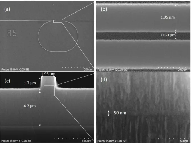
4.2 Porous silicon ridge waveguide MR fabrication
MRs based on PSi ridge waveguides have been manufactured from the 4-porous silicon layer structure using the process described in [19]. Following the fabrication steps, SEM measurements have been performed in order to verify the implementation of the PSi MRs. Figure 7 reports SEM images of a racetrack PSi MR with a radius R of 100 µm and a coupling length Lc of 70 µm. Moreover, in order to obtain a single-mode propagation for the TM polarization, the anodization time for the second barrier layer has been reduced to aim a thickness of 50 nm instead of the 280 nm previously chosen to facilitate its measurement by SEM observations and then to be able to adjust the experimental reflectance spectrum of the 4-layer system with the calculated one (figure 6).
The top view SEM image of the characterized MR is reported in Figure 7.a. The separation between the straight and the racetrack MR ridge waveguides, which appears in dark grey light (Figure 7.b), shows that the gap has been successfully made along the coupling length of the racetrack. A mean waveguide width of 1.95 µm instead of the targeted 2 µm was measured. The gap between the access waveguide and the resonant cavity is 0.6 µm, which is slightly higher than expected (0.5 µm) due to low side etching during the photolithography steps and already observed in previous studies [10, 19].
The cross section of the etched ridge waveguide is reported in Figure 7.c showing the PSi guiding and confinement layers with almost the aimed dimensions (1.7 µm and 4.7 µm respectively). The observation at a higher magnification allows to measure the thickness of the barrier layer between the guiding and the confinement PS layer at about 50 10 nm (figure 7.d).
12
Figure 7: SEM images of the racetrack micro-resonator: top views at different scales: (a) whole racetrack MR, (b) the gap separation between the straigth and the cavity waveguides of the coupling area, (c) cross section of a PSi ridge waveguide, and (d) estimation of the barrier layer thickness at higher magnification.
4.3 Optical simulations and characterizations
Before the optical characterizations of the fabricated PSi MR, some preliminary simulations of the waveguide schematized in figure 8.a have been carried out taking into consideration the experimental waveguide dimensions obtained by SEM observations. We have assumed a thickness of the first barrier layer of 30 nm with respect to the adjustment results of the theoretical and experimental reflectance spectra of the 4-layer PSi structure (figure 6). As the height of 1.7 µm of the guiding layer has been measured including the two barrier layers of 30 nm and 50 nm respectively (fig. 7.c and 7.d), we deduced the real height of 1.62 µm for the PSi core waveguide with a width of 1.95 µm (fig. 7.c).
Knowing the porosity, the refractive index evolution of each layer constituting the PSi waveguide could be determined as a function of the wavelength from the data in references [47, 48]. Then, from these data and considering the 4-layer PSi waveguide represented in figure 8.a, the effective index of the TM single propagated mode has been calculated with a FMM (Film Mode Matching) full vector Solver from FIMMWAVE software commercialized by Photon design. The FMM solver is a versatile numerical method for vector mode field
13
calculations and particularly adapted for waveguide structures with a rectangular geometry [49]. The effective index variation as a function of the wavelength has been fitted by a linear function over the studied range (figure 8.b) and the group index of the PSi waveguide has been deduced from equation (2) in the studied wavelength range: ng .
Figure 8: (a) Representation used in FIMMWAVE simulations of the 4-layer PSi waveguide constituted by a guiding layer sandwiched by two barrier layers and a confinement layer. The experimental dimensions have been taken into consideration. (b) FIMMWAVE calculated effective index evolution of the 4-layer PSi waveguide as function of the wavelength.
Effective refractive index have also been calculated as a function of the wavelength using Matlab software from the effective refractive index method [50], method that only consider a simple ridge waveguide constituted of a guiding and a confinement layer. Thus, using this method, we have neglected the upper and the lower technological barrier layers. This method is simple and regularly used in the field of integrated optics in the case of rectangular waveguides with low refractive index contrast (∆n 1) with a width/height ratio R >1. [51-53]. We have taken into consideration experimental waveguide dimensions: a width of 1.95 µm and a height of 1.7 µm. A group index of 1.646 0.001 in the studied wavelength range from 1.4 to 1.6 µm has been calculated, which is very close to the value determined by the FMM method, meaning that the barrier layers can be neglected.
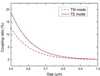
The coupling factor between the straight waveguide and the resonant cavity has been calculated at 1550 nm using Marcatili model [54]. This model is also regularly used in the field of integrated optics in the case of rectangular waveguides for low index contrast and dimensions for single mode propagation and not small enough compared to wavelength [55]. Precisions of the coupling factor determination method are given in [19]. The barrier layers are neglected again. The determined coupling factors for TE or TM modes are plotted as a function of the gap (separation distance between the access waveguide and the resonant cavity) in the range of 0.5 to 1 µm, that can be obtained from a process point of view (figure 9). We have taken into consideration experimental waveguide dimensions by neglecting the
14
upper and the lower barrier layers: a width of 1.95 µm, a height of 1.7 µm, a coupling length Lc = 70 µm and a radius R = 100 µm.
For the mean gap of 0.6 µm that is experimentally obtained (fig. 7.b), a coupling factor of about 8 % and 5 % have been calculated respectivley for the TE and TM modes (figure 9).
Figure 9: Calculated coupling factor as a function of the gap between the straight waveguide and the cavity respectively for the TE and TM modes for a waveguide width of 1.95 µm, a height of 1.7 µm at 1.55 µm and for the following cavity parameters R = 100 µm and Lc = 70
µm.
In order to verify that this fabricated PSi MR is optically operational, the spectral transmission was measured. Then, using the equations defined in our previous study on polymer micro-ring resonators [21], the theoretical transmission TM has been calculated and then adjusted to match the experimental one by varying the following parameters: group index, coupling ratio and optical losses.
Figure 10 reports the experimental and the theoretical adjusted spectral transmission responses. The experimental spectrum TM shows three resonance wavelengths in the studied range that are separated by a Free Spectral Range (FSR) of 1.93 nm, with , where L is the cavity perimeter ( ) and is the group index.
To match the experimental FSR, the group index ng was adjusted to 1.6551 ± 0.0001 which is
in good agreement with the previous group indices of 1.646 or 1.643 that have been calculated using Matlab or FIMMWAVE simulations respectively.
The adjustment of the resonance shape is performed by varying the coupling factor and the propagation losses in the resonant cavity. A coupling factor κ² of 5 ± 1 % and a field attenuation constant a = 0.8835, which corresponds to propagation losses per length unit (α) of 14.0 ± 0.4 dB/cm, have been obtained in this case. The value obtained for the coupling factor well corresponds well to that estimated for the TM mode. As the minimum of transmission resonant wavelenght is about 0.4 , the critical coupling is not reached.
A width at half-height (δλ) of 06 nm is obtained, with a corresponding quality factor Q of 2.5 104, which is better than those obtained in previous studies using another refractive indices [10, 19]. Morever, this quality factor could be yet improve by optimizing the coupling length to reach critical coupling and thus obtain a total extinction response at resonant wavelenghts.
15
Figure 10: Experimental and theoritical transmission spectra of the fabricated PSi MR and for the TM polarization.
A group refractive index and a coupling factor have been deduced from the theoretical adjustment of the experimental optical transmission of the PSi MR. The values are very close to those calculated using the refractive index of the PSi layers. These results validate the porosity calibration taking into consideration the thin barrier layer. They demonstrate again the influence of the barrier PSi layer on the porosities and so on the refractive indices of both the guiding and the confinement PSi layers.
As the PSi MR is dedicated to biosensing applications, an estimation of the surface sensititvy of the MR for a BSA (Bovin Serum Albumin) detection have been calculated using previous results [14, 32]. For biosensing, the PSi guiding layer has to be functionnalised for specific grafting of BSA molecule. Functionalization proccess of the PSi internal surface described in [32] has been used. It includes a silanization step using Aminopropyltriethoxysilane (APTES) and a coupling step using Glutaraldehyde (GL) molecules. We have supposed a functionalization of the PSi internal surface with one monolayer of APTES and one monolayer of glutaraldehyde to get the volume fraction of each component. Then using Bruggeman relation and modelling of the PSi surface described in [14], the refractive index of the functionalized PSi guiding layer has been determined. After BSA grafting step, the refractive index of the PSi guiding layer can also be deduced from Bruggeman model from a volume fraction of BSA (fBSA) which is correlated to MBSA, the number of molecules grafted
per surface unit of the functionalized PSi. MBSA can be estimated taking into consideration the
surface specific area (Ss) of 90 m²/cm3 calculated from [56], the volume of BSA (VBSA) of
125 nm3 [57] and the BSA molar weight (Mmol BSA) of 66.43 kDa [57]. The quantity of BSA
in pg/mm² graffed on the internal surface of pore (MBSA) is equal to
Surface sensitivity Ssurf. depends on the variation of the effective refractive index of the
propagated mode, taking into account the variation of the BSA mass per unit of surface (MBSA) grafted onto the waveguide PSi internal surface. Ssurf. is defined as [20]:
16
The refractive index of the waveguide confinement layer is assumed not to be affected by the functionalization process because of the presence of the second PSi barrier layer. The effective index of the TM mode of the PSi waveguide has been calculated by Matlab software using the effective refractive index method before and after BSA grafting on the internal surface of the PSi guiding layer. The calculation was carried out for a fBSA value of 0.1%
corresponding to a MBSA of 10 pg/mm² in order to get a corresponding wavelenght shift
inferior to the ISL of the MR.
A surface sensitivity of 0.06 nm / (pg/mm²) has been estimated which is slightly better than that estimated in a previous study [19, 20] with other porosity of the PSi guiding layer. As the quality factor is also better than those previously obtained in [20, 21], a lower limit of detection (LOD) could be obtained with the studied PSi MR. Taking into consideration a minimal shift corresponding to the width at half-height (δλ) of 0.06 nm, and a minimum wavelength resonant shift of δλ /10 [58], a promising LOD of 0.1 pg/mm² could be obtained.
Conclusion
In this paper, the porosity of the guiding and the confinement PSi layers have been determined by taking into consideration the influence of low porosity barrier layers required to fabricate a 4-layer PSi structure. This 4-layer PSi structure consisting of a guiding layer with a well-defined refractive index of 1.57 at 1.55 µm is required to subsequently fabricate a hybrid MR with of a PSi MR and a straight access waveguide made of SU8 polymer with the same refractive index. Two PSi barrier layers fabricated with a current density of 1 mA/cm² and sandwiching the guiding layer in the 4-layer waveguide structure are also necessary for the technological realization.
The presence of a barrier PSi layer influences the porosity and the anodization rate of the guiding and the confinement PSi layers: their porosities are lower than if these layers had been manufactured separately as a single layer and the anodization rate is on the contrary higher. This effect is amplified for higher current densities.
Taking into account the influence of a PSi barrier layer and the porosity calibration results, current densities of JG = 85 mA/cm² and JC = 110mA/cm² have to be applied in the
anodization process to obtain a guiding and confinement PSi layer with refractive index of 1.57 and 1.41 respectively.
The good fit of the experimental reflectance spectrum of the 4-layer PSi structure with a theoretical spectrum calculated from the SEM measurements and the targeted refractive indices certifies the validity of the porosity calibration.
Then a 4-layer PSi MR has been fabricated using these current densities. The parameters deduced from the adjustment of the experimental and theoretical MR transmissions are well consistent with those previously simulated from the target indices of 1.57 and 1.41 corresponding to the guiding and confinement PSi layers respectively.
The calibration of both the porosity and anodization rate of PSi layers taking into account the presence of barrier PSi layers is necessary for the future technological realization of the hydride MR that will be based on PSi and SU8 polymer.
17
Work will continue in our laboratory to focus on the manufacture of the hybrid MR. In parallel, the PSi layers will be functionalized for a specific grafting of molecules for biosensing applications. The calibration method which have been validated in this paper will be used to study the index variations at each step of the functionalization process as was done in reference [14]. Preliminary theoretical results of sensitivity for BSA detection of 0.06 nm/(pg/mm²) and a LOD of 0.1 pg/mm² are very promising.
Acknowledgments
This work is funded by Lannion Trégor Community (LTC22), Région de Bretagne. Technological processing of ridge waveguides was performed in the CCLO-Renatech clean room facilities of Institut Foton. Equipment funding of Institut Foton and CCLO was partly provided by the CPER Sophie
References
[1] L De Stefano, “Porous silicon optical biosensors: still a promise or a failure?”, Sensors,
19 (2019) 4476. DOI:10.3390/s19214776
[ ] A Jane, Dronov, A Hodges and N H Voelcker, “Porous silicon biosensors on the
advance”, trends in biotechnology, 7, n° ( 9) -239.
doi.org/10.1016/j.tibtech.2008.12.004
[3] F A Harraz, “Porous silicon chemical sensors and biosensors: A review”, Sensors and
Actuators B 202, (2014) 897-912. doi.org/10.1016/j.snb.2014.06.04
[4] S. Arshavsky-Graham, N. Massad- vanir, E Segal, S Weiss, “Porous silicon based photonic biosnesors: current status and emerging applications”, Anal Chem. 91 (2019)
441-467. DOI: 10.1021/acs.analchem.8b05028
[5] A. Loni, L.T. Canham, M.G. Berger, R. Arens Fischer, H. Munder, H. luth, H.F. Arrand, T.M. Benson, “Porous silicon multilayer optical waveguides”, Thin Solid Films 7 (1999 )
143-146.doi.org/10.1016/0040-6090(95)08075-9
[6] K. Kim and T.E Murphy, “Porous silicon integrated Mach-Zehnder interferometer waveguide for biological and chemical sensing”, Optics Express 1, n°17 (2013) 19488. DOI:10.1364/OE.21.019488
[7] T H Talukdar, G D Allen, Kravchenko and J D yckman, “Single-mode porous silicon waveguide interferometers with unity confinement factors for ultrasensitive adlayer
sensing”, Optics Express, 27, n°16 (2019) 22485.doi.org/10.1364/OE.27.022485
[8] X. Wei and S. Weiss, “Guided mode biosensor based on grating coupled porous silicon
18
[9] G A odriguez, H Shuren, S M Weiss, “Porous silicon ring resonator for compact, high sensitivity biosensing applications”, Optics Express , n° (2015) 7111-7119. doi.org/10.1364/OE.23.007111.
[10] P. Girault, P. Azuelos, N. Lorrain, L. Poffo, J. Lemaitre, P. Pirasteh, I. Hardy, M. Thiual, M Guendouz and J Charrier, “Porous silicon micro-resonator implemented by standard photolithography process for sensing application”, Optical Materials, 72 (2017) 596 – 601. doi.org/10.1016/j.optmat.2017.07.005.
[11] G. A. Rodriguez, P. Markov, A. P. Cartwright, M. H. Choudhury, F. O. Afzal, T. Cao, S. I. Halami, S. T. Retterer, Kravchenko and S M Weiss, “Photonics crystal naobeam biosensors based on porous silicon”, Optics Express, 27, n° 7 (2019) 9536-9549. doi.org/10.1364/OE.27.009536
[12] M. Arroyo-Hernandez, R.J. Martin-Palma, V. Torres-Costa, J.M. Matinez Duart, “Porous silicon optical filters for biosensing applications”, Journal of non-crystalline Solids, 352
(2006) 2457-2460. doi: 10.1016/j.jnoncrysol.2006.02.075
[13] L. Moretti, I. Rea, L. De Stefano and I. Rendina, “Periodic versus aperiodic: Enhancing the sensitivity of porous silicon based optical sensors”, Appl Phys Lett 90, (2007) 191112.
doi.org/10.1063/1.2737391
[14] N. Lorrain, M. Hiraoui, M. Guendouz, L Haji, “Functionalization control of porous silicon optical structures using reflectance spectra modeling for bio sensing applications”,
Material Science and Engineering B 176, (2011) 1047-1053.
doi.org/10.1016/j.mseb.2011.05.040.
[15] F S H Krismastuti, S Pace and N H Voelcker, “Porous silicon resonant microcavity biosensor for matrix metalloproteinase detection”, Advanced functional materials, 24 (2014)
3639-3650.DOI: 10.1002/adfm.201304053.
[16] K. A. Kilian, T. Böcking, L. M. H. Lai, S. Ilyas, K. Gaus, M Gal, “Organic modification of mesoporous silicon rugate filters: the influence of nanoarchitecture on optical behaviour”,
Int. J. Nanothechol., 5, n°2/3 (2008) 170 – 178.DOI: 10.1504/IJNT.2008.016914
[17] C.Y.Chao and L. J. Guo, “Design and Optimization of microring resonators in biochemical sensing applications”, Journal of lightwave technology, 24, n°3 (2006)
1395-1402. DOI: 10.1109/JLT.2005.863333.
[18] N Jokerst, M oyal, S Palit, L Luan, S Dhar and T Tyler, “Chip scale integrated
microresontor sensing systems”, Journal of Biophotonics, , n° ( 9) 1 -226. DOI
10.1002/jbio.200910010.
[19] P. Girault, N. Lorrain, J. Lemaitre, L. Poffo, M. Guendouz, I. Hardy M. Gadonna A. Gutierrez, L. Bodiou, J. Charrier “ acetrack micro-resonators based on ridge waveguides made of porous silica”, Optical Materials, 50 (2015) pp. 167-174.
doi.org/10.1016/j.optmat.2015.10.017.
[20] P. Azuelos, P. Girault, N. Lorrain, Y. Dumeige, L. Bodiuo, L. Poffo, M. Guendouz, M. Thual and J Charrier, “Optimization of porous silicon waveguide design for microring resonator sensing applications”, Journal of Optics, , n°8 ( 18) 85 1 doi.org/10.1088/2040-8986/aad01b.
19
[21] P. Girault, N. Lorrain, L. Poffo, M. Guendouz, J. Lemaitre, C. Carré, M. Gadonna, D. Bosc and G Vignaud, “ ntegrated polymer micro-ring resonators for optical sensing applications”, Journal of Applied Physics, 117 ( 15) 1 5 doi.org/10.1063/1.4914308
[22] K K Tung, W H Wong, E Y B Pun, “Polymeric optical waveguides using direct ultraviolet photolithography process”, Applied Physics A 8 , ( 5) 1-626. DOI: 10.1007/s00339-003-2248-8.
[23] G Vincent, “Optical properties of porous silicon supperlattices”, Applied physics letters,
64 (1994) 2367 – 2369.doi: 10.1063/1.111982
[24] R.J. Martin-Palma, V. Torres-Costa, M. Arroyo-Hernandez, M. Manso, J. Perez-Rigueiro, J.M. Martinez-Duart, “Porous multilayers stacks for optical biosensing applications”, Microelectronics Journal, 5 ( ) 5-48. doi:10.1016/S0026-2692(03)00216-7.
[25] V. Torres – Costa, R.J. Martin-Palma, J.M. Martinez-Duart, “Optical characterization of porous silicon films and multilayer filters”, Applied physics A, 79 ( ) 1919-1923. DOI: 10.1007/s00339-004-2642-x
[26] R. Nava, M.B. dela Mora, J. Tagüena-Martinez and J A del io, “ efractive index contrast in porous silicon multilayers”, Phys Status Solidi C, 6, n°7 (2009) 1721 – 1724. DOI 10.1002/pssc.200881090
[27] C Mazzoleni and L Pavesi, “Application to optical components of dielectric porous silicon multilayers”, Applied Physics Letters, 7, n° , (1995) 98 -2985. doi.org/10.1063/1.114833
[28] M.G. Berger, M. Thönissen, R. Arens-Fisher, H. Münder, H. Lüth, M. Arntzen, W. Thei, “ nvestigation and design of optical properties of porosity superlattices”, Thin Solid Films, 255 (1995) 313-316. doi.org/10.1016/0040-6090(94)05617-M
[29] L Pavesi, “Porous silicon dielectric multilayers and microcavities”, icista del nuovo cimento, 20, n°10 (1997) 1-76. doi.org/10.1007/BF02877374
[30] M. Hiraoui, L. Haji, M. Guendouz, N Lorrain, A Moadhen, M Oueslati, “Towards a biosensor based on anti resonant reflecting optical waveguide fabricated from porous silicon”, Biosensors and Bioelectronics 36 (2012) 212 - 216. DOI :10.1016/j.bios.2012.04.022
[31] J E Lugo, H A Lopez, S Chan and P M Fauchet, “Porous silicon multilayers structures: A photonic band gap analysis”, Journal of applied physics, 91, n°8 ( ) 9 - 4972. doi: 10.1063/1.1461898.
[32] M Hiraoui, M Guendouz, N Lorrain, A Moadhen, L Haji, M Oueslati, ‘Spectroscopy studies of functionalized oxidized porous silicon surface for biosensing applications», Materials Chemistry and Physics 128 (2011) 151 - 156. doi: 10.1016/j.matchemphys.2011.02.052
[33] C. Xiao, R. Boukherroub, J. T. C. Wojtyk, D. D. M. Wayner, and J. H. T. Luong. "Structure characterization of porous silicon layers based on a theoretical analysis". Langmuir,
20
[34] D. S. Bethune. "Optical harmonic generation and mixing in multilayer media: analysis using optical transfer matrix techniques". J. Opt. Soc. Am., vol. 6, 1989, pp. 910, doi.org/10.1364/JOSAB.6.000910
[35] D. A. G. Bruggeman. "Berechnung verschiedene physikalischer konstanten von heterogenen substanzen". Ann. Phys., vol. 5, 1935, pp. 636.doi.org/10.1002/andp.19354160705
[36] A M Campos, J Torres and J J Giraldo, “Porous silicon dielectric function modeling from effective medium theories”, Surface eview and Letters, Vol 9, n°5-6 (2002) 1631-1635. doi.org/10.1142/S0218625X02004116
[ 7] A Halimaoui, “Determination of the specific surface area of porous silicon from its etch rate in HF solutions”, Surface Science Letters 306 (1994) L550-L554. doi.org/10.1016/0039-6028(94)91176-2
[38] Halimaoui A. “Porous silicon: material processing, properties and applications” in Porous
Silicon : Science and Technology, Vial J. C. and Derrien J. (eds), Berlin, Springer Verlag, and Les Ulis, Les Editions de Physique, 1995, pp. 33-52.
[39] J. Charrier, Y. Dumeige, P. Pirasteh and M. Gadonna, Effect of interface roughness and polarization on the optical losses of porous silicon-based waveguides, IET Micro&Nano Letters 7(3) (2012) 275-278. doi.org/10.1049/mnl.2012.0027.
[40] S Setzu, G Lerondel and omestain, “Temperature effect on the roughness of the formation interface of p-type porous silicon”, J App Phys , 8 , (1998) 1 9-3133. doi.org/10.1063/1.368467
[41] C.F. Ramirez-Gutierrez, J.D. Castaño-Yepes and M.E. Rodriguez-Garcia, “ n situ photoacoustic characterization for porous silicon growing: Detection principles”, J Appl Phys, 119 (2016) 185103. doi.org/10.1063/1.4948946
[42] C.F. Ramirez-Gutierrez, J.D. Castaño-Yepes and M.E. Rodiguez-Garcia, “Optical interferometry and photoacoustics as in-situ techniques to characterize the porous silicon formation: a review”, Open Mater Sci , ( 18) -32. doi.org/10.1515/oms-2018-0003 [43] C.F. Ramirez-Gutierrez, H.D. Martinez-Hernadez, Y. A. Lujan-Cabrera and M. E. Rodriguez-Garcia, “Design, fabrication, and optical characterization of one dimensional photonic crystals based on porous silicon assisted by in-situ photoacoustics”, Scientific reports, 9, (2019) 14732. doi.org/10.1038/s41598-019-51200-1
[44] I.A. Lujan-Cabrera, C.F. Ramirez-Gutierrez, J.D. Castaño-Yepes, M.E. Rodriguez-Garcia, “Effects of the interface roughness in the optical response of one dimensional photonic crystals of porous silicon”, Physica B: Condensed Matter 560 (2019) 133-139. doi.org/10.1016/j.physb.2019.02.010
[45] Y-S. Ghim, H-G hee and A Davies, “Simultaneous measurements of top surface and its underlying film surfaces in multilayer film structure”, Scientific reports, Vol 7 ( 17) 11843
DOI:10.1038/s41598-017-11825-6
[46] R. Santbergen, A. H.M. Smets and M Zeman, “Optical model for multilayer structures with coherent, partly coherent and incoherent layers”, Optics Express, vol 1, n°S ( 1 ) A2462-A267. doi.org/10.1364/OE.21.00A262.
21
[47] C. D. Salzberg and J. J. Villa. Infrared Refractive Indexes of Silicon, Germanium and Modified Selenium Glass, J. Opt. Soc. Am., 47 (1957) 244-246 doi.org/10.1364/JOSA.47.000244.
[48] B. Tatian. Fitting refractive-index data with the Sellmeier dispersion formula, Appl. Opt. 23 (1984) 4477-4485. doi.org/10.1364/AO.23.004477.
[49] A.Sv. Sudbo, “Film mode matching : a versatile numerical method for vector mode filed calculations in dielectric waveguides”, Pure Appl Opt (199 ) 11-233.DOI: 10.1088/0963-9659/2/3/007
[50] A B Fallahkhair, K S Li, T E Murphy, “Vector finite difference mode solver for anisotropic dielectric waveguides”, Journal of lightwave technology, , n°11 ( 8) 1 -1431.DOI : 10.1109/JLT.2008.923643
[51] K S Chiang, “Performance of the effective-index method for the analysis of dielectric waveguides”, Optics Letters, 1 , n°1 (1991) 71 – 716. doi.org/10.1364/OL.16.000714 [52] D V Batrack, S A Plisyuk, “Applicability of the effective index method for sumilatinf ridge optical waveguides”, Quantum electronics , n° , ( ) 9-352. DOI:10.1070/QE2006v036n04ABEH013149
[5 ] W M Berrouane, M Anani, A Chama, C Mathieu, “Effective index method applied on a GaN/InxGa1-xN integrated optics waveguide”, nternational Journal of Nanoelectronics and Materials, 11, n°. 3 (2018) 311-320.
[54] E. A. J. Marcatili, “Dielectric ectangular Waveguide and Directional Coupler for ntegrated Optics”, The Bell System Technical Journal, Vol 48, Issue 7 (1969) pp. 2071-2102. doi.org/10.1002/j.1538-7305.1969.tb01166.x
[55] G Hunsperger, “ ntegrated optics: Theory and Technology”, Springer-Verlag Berlin Heidelberg (1995). doi: 10.1007/978-3-662-13521-1
[56] M Dribek, J Charrier, “Theoretical study of the factor of merit of porous silicon based optical biosensors” Journal of Applied Physics 1 7 ( 1 ) 9 5-1 – 044905-10. DOI:10.1063/1.3295906.
[57] F L G Flecha, V Levi, Biochem “Determination of the molecular size of BSA by fluorescence anisotropy”, Mol Biol Educ 1 (5) ( ) 19–322. doi.org/10.1002/bmb.2003.494031050261
[58] L. M. Lechuga, “Biosensors and modern biospecific analytical techniques”, in Elsevier, 2005, chap. Optical biosensors, pp. 209.