Publisher’s version / Version de l'éditeur:
Nano Letters, 17, 1, pp. 322-327, 2016-12-05
READ THESE TERMS AND CONDITIONS CAREFULLY BEFORE USING THIS WEBSITE. https://nrc-publications.canada.ca/eng/copyright
Vous avez des questions? Nous pouvons vous aider. Pour communiquer directement avec un auteur, consultez la
première page de la revue dans laquelle son article a été publié afin de trouver ses coordonnées. Si vous n’arrivez pas à les repérer, communiquez avec nous à [email protected].
Questions? Contact the NRC Publications Archive team at
[email protected]. If you wish to email the authors directly, please see the first page of the publication for their contact information.
NRC Publications Archive
Archives des publications du CNRC
This publication could be one of several versions: author’s original, accepted manuscript or the publisher’s version. / La version de cette publication peut être l’une des suivantes : la version prépublication de l’auteur, la version acceptée du manuscrit ou la version de l’éditeur.
For the publisher’s version, please access the DOI link below./ Pour consulter la version de l’éditeur, utilisez le lien DOI ci-dessous.
https://doi.org/10.1021/acs.nanolett.6b04125
Access and use of this website and the material on it are subject to the Terms and Conditions set forth at
Quantum transport in gated dangling-bond atomic wires
Bohloul, S.; Shi, Q.; Wolkow, Robert A.; Guo, Hong
https://publications-cnrc.canada.ca/fra/droits
L’accès à ce site Web et l’utilisation de son contenu sont assujettis aux conditions présentées dans le site LISEZ CES CONDITIONS ATTENTIVEMENT AVANT D’UTILISER CE SITE WEB.
NRC Publications Record / Notice d'Archives des publications de CNRC:
https://nrc-publications.canada.ca/eng/view/object/?id=a23f6f09-d7bd-4312-ad4d-4b1ba32e3fd0 https://publications-cnrc.canada.ca/fra/voir/objet/?id=a23f6f09-d7bd-4312-ad4d-4b1ba32e3fd0
Quantum Transport in Gated Dangling-Bond Atomic Wires
S. Bohloul,
*
,†Q. Shi,
†Robert A. Wolkow,
‡,¶and Hong Guo
††
Center for the Physics of Materials and Department of Physics, McGill University, Montreal, Quebec H3A 2T8, Canada
‡
National Institute for Nanotechnology, National Research Council of Canada, Edmonton, Alberta T6G 2M9, Canada
¶
Department of Physics, University of Alberta, Edmonton, Alberta T6G 2E1, Canada
*
S Supporting InformationABSTRACT: A single line of dangling bonds (DBs) on Si(100)-2 × 1:H surface forms a perfect metallic atomic-wire. In this work, we investigate quantum transport properties of such dangling bond wires (DBWs) by a state-of-the-art first-principles technique. It is found that the conductance of the DBW can be gated by electrostatic potential and orbital overlap due to only a single DB center (DBC) within a distance of ∼16 Å from the DBW. The gating effect is more pronounced for two DBCs and especially, when these two DB “gates” are within ∼3.9 Å from each other. These effective length scales are in excellent agreement with those measured in scanning tunnelling microscope experiments. By analyzing transmission
spectrum and density of states of DBC−DBW systems, with or without subsurface doping, for different length of the DBW, distance between DBCs and the DBW, and distance between DB gates, we conclude that charge transport in a DBW can be regulated to have both an on-state and an off-state using only one or two DBs.
KEYWORDS: Dangling bond nanowires, interconnects, atomic scale switch, quantum transport
O
ngoing miniaturization of electronic devices strongly depends on discovering, fabricating, and characterizing nanoscale structures. Recent advances in creating and controlling silicon dangling bonds (DBs) with atomic precision1−7 have pushed this endeavor to truly atomic scale.On a hydrogen (H) terminated Si(100)-2 × 1:H surface, a DB is created by removing a single H atom. Such a DB center (DBC) introduces localized surface states at the middle of the Si(100)-2 × 1:H band gap, where these localized states are well decoupled from the electronic structure of the underneath substrate.1,8−15Engineering these midgap states is a powerful
method for constructing atomic-scale structures having potential applications as quantum dots (QD),1 room temper-ature cellular automata (QCA),1,16,17 interconnects,5,18,19 quantum information processing units,20,21etc.
A single line of such DBs on Si(100)-2 × 1:H surface exhibits a metallic behavior, as concluded by theoretical calcula-tions.9,18,19,22−28 Since in principle all DBs are precisely
identical in all physical aspects, hence utilizing DB-wires (DBWs) is a perfect way for achieving atomic wires in the ultimate size limit18 with similar functionality. It is very interesting to investigate the possibility of assembling functional systems by these perfect DBWs. To this end, the first and most important issue is to understand how charge transport along such a DBW can be controlled by a gate potential. While it is perhaps feasible to fabricate, by the most advanced nano-fabrication techniques, a metal gate that capacitively couples to a DBW, a very exciting alternative is to gate the DBW by a single DBC or a few DBCs nearby. According to scanning tunnelling microscope (STM) experiments of ref 15, which
studies interaction between different configurations of DBs on Si(100)-2 × 1:H surface by probing corresponding density of states (DOS), a single DB can strongly influence DOS of nearby line of DBs. However, a direct charge transport measurement along such a line of DBs (DBW) is yet to be carried out. It is the purpose of this work to theoretically investigate quantum transport properties of DBWs gated by DBC using a state-of-the-art first-principles technique.
To accurately determine quantum transport properties of gated DBWs or, in fact, any semiconductor nanostructures, first-principles methods face three main challenges. First, density functional theory (DFT) at local density approximation (LDA) or generalized gradient approximation (GGA) levels can not correctly determine band gaps,29making the calculated results questionable at these levels of theory. Second, experimentally it is shown1,21 that a DB interacts with its surroundings up to a distance of ∼16 Å, which demands systems with large number of atoms for first-principles calculations. Third, experimental systems contain randomly distributed impurity dopant atoms, which in principle requires one to obtain disorder configuration average of any calculated quantity. To the best of our knowledge, these theoretical challenges have not been overcome before. In our work, we meet these challenges by using a state-of-the-art first-principles approach where DFT is carried out within the nonequilibrium Green’s function (NEGF) formalism. Our NEGF-DFT method Received: October 1, 2016
Revised: November 23, 2016 Published: December 5, 2016
correctly determines the band gap and electronic structures of Si(100)-2 × 1:H surface by a semilocal exchange potential, it is extremely efficient such that gated DBW systems with up to 4872 Si atomic sites were investigated, and the doping disorder is handled by an advanced nonequilibrium coherent potential approximation (NECPA). This powerful first-principles technique allows us to self-consistently and quantitatively predict quantum transport properties of gated DBWs sitting on doped Si(100)-2 × 1:H surfaces.
Our results show that quantum transport in gated DBW is markedly different from that without gating, indicating significant electrical control of charge current, even though the gate is only a single DB. We found that the transmission spectrum of DBW is tunable by factors such as the number of nearby DBCs acting as a gate, the distance between DBC and DBW, as well as the interseparation distance between gating DBCs. Our calculation indicates a direct coupling interaction between DBC and DBW up to a distance of ∼16 Å, consistent with findings in STM experiments.1,15
Before presenting the results, we briefly outline the NEGF-DFT technique used in this work. The NEGF-NEGF-DFT formalism, known as the most widely applied method for calculating quantum transport properties from atomic point of view,30 consists of carrying out a DFT-like self-consistent analysis with a density matrix obtained by NEGF. We refer interested readers to the original literature for details of this formalism.30,31In this work, the modified Becke−Johnson semilocal exchange potential32 is used in our NEGF-DFT calculation, which correctly determines band gap of many semiconductors and insulators, band dispersions,33and band offsets.34In particular, it correctly produces 2.0 eV band gap of Si(100)2 × 1:H surface.6 Furthermore, for capturing the effect of impurity atoms and configurational average process, we use a recently developed nonequilibrium coherent potential approximation (NECPA) theory,35,36which avoids the brute force computa-tion by analytically deriving an ensemble averaged transmission coefficient in terms of averaged Green’s functions and vertex corrections due to multiple impurity scattering.35,36 NECPA theory allows configurational averaged physical quantities to be obtained by only a single first-principles numerical calcu-lation.37−41 These theoretical approaches have been
imple-mented in NEGF-DFT quantum transport simulation package Nanodsim,42 which is based on linearized muffin-tin orbital (LMTO) flavor of DFT within atomic sphere approximation (ASA) to drastically enhance the computation efficiency. This allows us to consider systems as large as 4872 Si atomic sites in the self-consistent NEGF-DFT iteration for investigating the gating effect of a DBW.
We start by optimizing an eight layer Si(100)-2 × 1:H slab fully terminated at the top and bottom by H atoms. The optimization unit cell includes a vacuum region of ∼13 Å in the out-of-plane direction to isolate the periodic images of the slab. More details on the structure can be found in Supporting Information. Structural relaxation is performed using the projector augmented wave (PAW) method as implemented in VASP electronic package43 with a planewave cutoff of 430 eV, an 11 × 5 × 1 k-mesh according to the Monckhorst−Pack scheme,44 and LDA as exchange-correlation, until residual forces are smaller than 0.01 eV/Å per atom.
To build a two-probe DBW transport junction, the relaxed Si(100)-2 × 1:H unit cell is first widened three times in the x-direction to construct the yellow dashed-line region shown in Figure 1a. This dashed region is then periodically extended to z
= ±∞ to obtain the corresponding transport computational box as shown in Figure 1a,b. The infinitely long transport junction is naturally divided into three regions: left/right leads, which respectively extend to z = ±∞, and a central scattering region. It is only in this central region where gating DBCs and randomly distributed impurity atoms reside. These regions are shown by different colored atomic spheres in Figure 1a,b in which the DBW is shown45 as the chain of red spheres extending from z = −∞ to +∞. In NEGF-DFT analysis, the transport junction is periodic along x,y directions. Importantly, periodic images of DBWs along the x-direction are ∼23 Å apart from each other and a large vacuum is included in out-of-plane
y-direction, which provides excellent isolation of periodic
images of DBWs. Even though such a periodic extension helps to significantly reduce the size of the system by using k-sampling along x,y-directions, the number of atoms included in our self-consistent NEGF-DFT method, i.e., those in central scattering region and buffer layers (see Figure 1), is still extremely large from first-principles point of view. The Fermi level across the two probe structure is aligned by doping the leads to the same impurity concentration as central scattering region using virtual crystal approximation (VCA).46 The LMTO-ASA method used in NEGF-DFT transport calcu-lations utilizes an s,p,d basis including nine orbitals per atomic site. More details of the ASA and its accuracy are included in theSupporting Information. Finally, a 3 × 1 × 15 k-mesh is used for calculating the line-width functions of the device leads, a 3 × 1 k-mesh for converging self-consistent NEGF-DFT two-probe transport structure, and a 4 × 1 k-mesh in evaluating the transmission coefficient where all the mesh sizes are verified to produce converged numerical results.
Before presenting the result for gated DBWs, we start by examining transmission function T(E) versus electron energy E for DBWs of 3 to 10 DBs long (∼7.7 to ∼34.6 Å).Figure 2a shows calculated T(E) of an ideal DBW (without any impurity doping in the Si surface), which actually does not depend on DBW length, as expected from ballistic transport. T(E) of these Figure 1.(a) Top view and (b) side view (at wire’s cross-section) of the two-probe transport junction. The supercell used for constructing the two-probe system is shown within the dashed-yellow line box (∼23 Å in width), which is three times as large as a Si(100)-2 × 1:H unit-cell in the x-direction. The two-probe structure is generated by repeating the supercell box to z = ±∞, and it has three parts: the left/ right leads, the left/right buffer layers, and the central scattering region. NEGF-DFT self-consistent calculation includes all the atoms of the latter two parts. The Si and H atoms and DB are represented by blue (green in leads), white, and red spheres, respectively. Impurity atoms are randomly distributed in central scattering region (gray spheres). DBWs with lengths ranging from 3DB to 10DB (∼7.7 to ∼34.6 Å) are investigated.
Nano Letters Letter
DOI:10.1021/acs.nanolett.6b04125
Nano Lett.2017, 17, 322−327
ideal DBWs is divided into a 1-channel and a 2-channel energy range, providing 1 and 2 propagating Bloch states, respectively. In order to further analyze these energy channels, we calculate projected density of states (PDOS) at three different energy points, indicated by E1, E2, and E3 inFigure 2a. According to Figure 2b,c, PDOS shows that in 1-channel energy range (i.e., points E1, E2), transport states are largely localized over surface
DBs with only minor extension beneath the surface atoms, namely, the current is confined to the width of a single Si atom, forming a one-dimensional (1D) surface current. This behavior can be attributed to through-space coupling of DB orbitals.24,25 However, in 2-channel energy range (i.e., point E3) there is a
second propagating state (in addition to highly localized state over DBs), which spans over a larger surface area and penetrates into the substrate for about 2 Si layers, thus the electric current is partially carried by both the DBW and adjacent Si atoms in the subsurface.
Having understood transport characteristics of ideal DBWs, we now investigate the role of impurity doping by randomly inserting n-type (phosphorus) and p-type (boron) dopant atoms in central scattering region of two-probe transport junction (see Figure 1), at experimentally1 reported concen-trations of ∼5 × 1019cm−3and ∼1 × 1020cm−3. As is shown in Figure 3a,b, transmission is decreased by increasing the impurity concentration. This effect is larger in 2-channel energy range, which is due to the fact that its transport states extend beneath the surface where impurity atoms are located. Furthermore, as can be seen in Figure 3c,d, increasing the length of DBW at a fixed impurity concentration lowers the transmission in the same fashion, which is due to a higher number of scattering centers available in the system corresponds to longer DBW.
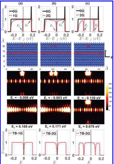
After presenting transport properties of ideal DBWs and DBWs on doped surfaces, we now investigate gating effect of DBCs located in vicinity of a DBW. These DBCs can be created intentionally in experimental devices. According to Figure 4a, placing a DBC at a distance of ∼7.69 Å from the DBW causes major variations in T(E), indicated by a sharp drop at E1 as well as a complete removal of the second
transport state in 2-channel energy range, i.e., a DBC creates a strong gating effect to the DBW. This effect is due to coupling between continuously propagating states on the DBW and localized states on the DBC. A DBC can be considered as an
atomic size quantum dot (QD) that interacts with its surrounding medium. For the DBW−DBC system shown in Figure 4a, quantum levels of DBC are broadened due to interaction with the DBW where peak of DOS is located at E1.
Consequently, for injected electrons at a given energy, final transport coefficient is determined by amount of DOS available at DBC as well as DBW−DBC coupling strength, which depends on spatial extension of continuum and localized states of the wire and DBC, respectively. In particular, T(E) drops to essentially zero at energy E1≈ 0 since DBC has a large DOS at the same energy (see the panels inFigure 4a). The large DOS of DBC at this energy provides a large coupling to the DBW, which affects the transport consequently. In addition, the second transport state in 2-channel energy range is highly suppressed because its larger spatial extension allows a strong coupling to the DBC, even if the DBC only provides a small DOS at energy E2. We also observe that displacing the single
DBC parallel to the wire, while keeping the DBW−DBC distance fixed, precisely results in the same T(E). Quantita-tively, by moving the DBC away from the DBW, our calculation predicts that the gating effect vanishes for DBW−DBC distances larger than dc ≈ 15.4 Å. This predicted dc value is in excellent agreement with several experimental reports that analyzed interactions of DB clusters using STM.1,15
The gating effect can be tuned by including a second DBC, say at the same distance from the wire. Our calculation shows that these two DBCs are essentially uncoupled when their interseparation distance is larger than ∼7.7 Å. Once uncoupled, they act as two identical atomic QDs having the same energy levels. Therefore, as can be seen in Figure 4b, this combined system still contains only one DOS peak at E1, although it is
distributed over two different locations on the surface, corresponding to two DBCs. This in turn causes only one major drop in T(E1): though it could not be discerned inFigure 4b, T(E1) numerically drops to a smaller value in comparison to
the case of one DBC. In other words, when two DBCs are far apart (thus uncoupled), they generate a gating effect rather similar to the system with one DBC.
We also observe that reducing the interseparation distance of DBCs results in their coupling with each other. For instance, at distance of 3.9 Å, a strong DBC−DBC coupling splits the degenerate energy levels of DBC into two distinct energy levels with major DOS at E1and E2(seeFigure 4c). This explains the
Figure 2.(a) Transmission spectrum T(E) of a 34.6 Å long DBW containing 10 DBs (10DBW) on clean Si(100)-2 × 1:H. The Fermi level is shifted to the origin of energy E. Transport due to substrate valence (conduction) band starts at ∼−1.12 eV (∼0.62 eV), while the nonzero T(E) within the gap region (from ∼−0.26 eV to ∼0.20 eV) is due to midgap states of the DBW. T(E) of a DBW has two distinct energy regions based on the number of available transport channels: a 1-channel energy range (e.g., energies like E1and E2) and a 2-channel energy range (E3). (b) Top view and
(c) side view of color-coded PDOS corresponding to the three energies E1, E2, and E3. Brighter spots indicate regions with higher DOS in the
system. In 1-channel energy range, transport is highly localized on the DBW; whereas in 2-channel energy range, transport penetrates into the substrate for about two Si layers and spans over a larger surface area.
appearance of two dips47at E1and E2in T(E) since now the
combined DBC−DBW system provides two DOS peaks at two different energy points. We also observe an interesting anisotropic interaction between DBs on Si(100)-2 × 1:H surface: while DBC−DBW couples (an interaction perpendic-ular to dimers row) up to a distance of ∼16 Å, DBCs only couple with each other (an interaction along dimers row) within a distance of ∼3.9 Å. Therefore, on Si(100)-2 × 1:H
surface, DBs interact significantly stronger in direction perpendicular to the dimer row than along it. This anisotropy is also observed in experimental STM measurements studying interaction between DBs on Si(100)-2 × 1:H surface.15
In order to further demonstrate the nature of the gating mechanism, in the Supporting Information, we introduce a tight-binding model consisting of a linear chain of single orbital “atoms” coupled to identical one-orbital DBCs. By fitting appropriate parameters to our first-principles results, main features of NEGF-DFT results shown in Figure 4 are reproduced. More information regarding this tight-binding model is provided in theSupporting Information.
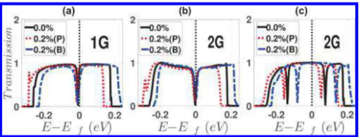
Finally,Figure 5shows T(E) of DBW−DBC systems in the presence of p-type (B) and n-type (P) dopants randomly distributed in the substrate. General transport features are Figure 3.T(E) of 10DBW in the presence of (a) n-type (phosphorus)
and (b) p-type (boron) impurity doping in the substrate. Experimentally reported concentrations of ∼5 × 1019 cm−3 (0.2%)
and ∼1 × 1020cm−3(0.4%) are shown by dotted-blue and
dashed-green lines, respectively. Also, T(E) of the corresponding clean system is shown by a solid-red line for comparison. Impurity scattering slightly decreases T(E), and the effect is relatively larger for the 2-channel energy range. Transmission curves are shifted to the left (right) due to the n-type (p-type) doping. (c,d) T(E) of n-type and p-type systems where, for a fixed 0.4% impurity concentration, the length of DBW is increased from 3 DBs to 5DBs to 10 DBs (7.7 to 34.6 Å) shown by solid-red, dotted-blue, and dashed-green lines, respectively.
Figure 4.(a) T(E) of a 10DBW gated by a single DBC located at 7.7 Å from the wire, together with the schematic of corresponding system and calculated PDOS at E1and E2(vertical panels). The legend “0G,
1G, 2G”′ means zero to two DBC gates. Also, the wire and the DBCs are shown by red spheres. The gated DBW has a transmission dip at
E1, which persists to a distance of ∼16 Å between the DBW and DBC.
Large DOS provided by the gate at E1can be seen as the bright spot
located at gate’s position in related PDOS panel. (b) T(E) with two DBCs located at 7.7 Å from the wire, where the two DBCs are 7.7 Å apart from each other. (c) T(E) with two DBCs at ∼7.7 Å from the wire, but ∼3.9 Å apart from each other, the strong coupling between the two DBCs gives rise two distinct transmission dips that are perfectly correlated with the overlapping DOS peaks at E1 and E2
(third panel). In the fourth panels, tight-binding results are shown that qualitatively capture the main transport features of gated DBW.
Nano Letters Letter
DOI:10.1021/acs.nanolett.6b04125
Nano Lett.2017, 17, 322−327
preserved although impurity scattering slightly alters T(E). As can be seen inFigure 5a,b, transmission dips still appear at the Fermi level in doped systems. As we expect, p-type (n-type) doping shifts the Fermi level down (up). Since energy levels of DBCs experience the same shift, DOS peak on DBCs remains at the Fermi level of the system. This also causes a shift in split energy levels of coupled DBCs since their energy level as an DBC is now changed due to doping (seeFigure 5c).
In conclusion, T(E) of DBWs fabricated on Si(100)-2 × 1:H surface can be divided into a 1-channel and a 2-channel energy range. In 1-channel range, transport states are highly localized on the DBW; in 2-channel range they are spanned over a larger surface area and also penetrate into the substrate. As a result, impurity scattering from dopant atoms, which are distributed within the substrate, leads to a small reduction of transmission along the DBW with relatively a larger impact in 2-channel energy range. Importantly, this finding suggests a good stability of surface current carried by the DBW. Furthermore, existence of DBCs up to a distance of ∼16 Å from the wire strongly alters
T(E), which is characterized by appearance of transport dips.
Utilizing this effect provides a completely new way for gating the DBW by only using atomic-size DBCs. Our results show that this gating effect is entirely controlled by number of DBCs, their distance from the wire, and corresponding distance separating DBCs from each other. We also predict that, on Si(100)-2 × 1:H surface, interaction between DBs perpendic-ular to the dimer row is stronger than their interaction along the dimer row, with effective distances up to ∼16 and ∼3.9 Å, respectively. Our first-principles calculations are in excellent agreement with several STM experimental studies regarding interaction of DBs on Si(100)-2 × 1:H surface. Given the narrow energy width of T(E) (∼0.45 eV) and sharp transport dips at very small values (∼10−3) in DBC−DBW systems, our
proposed gating mechanism could provide a promising approach for achieving low power electronic switches at atomic limit. In general, tuning the energy levels of the DBC(s) can be used to switch between “on” and “off” states of such an atomic system. For example, capping or uncapping the DBC gate by absorbing or desorbing a molecule17 results in removal or reappearance of the DBC state, hence switching between the “on” and “off” states of the DBW. This suggests application of DBC−DBW system as a single molecule detector. Calibration of such a single molecule sensor can be done against other effects such as the molecule landing on the DBW itself. Another interesting possibility is to exploit the sharp features of the
T(E) near the Fermi level in the DBW−DBC system for
thermoelectric effects since the Seebeck coefficient is propor-tional to dT/dE. In this way, the results presented in this work point to the attractive possibility of engineering controllable atomic-scale devices with desired functionality.
■
ASSOCIATED CONTENT*
S Supporting InformationThe Supporting Information is available free of charge on the ACS Publications website at DOI: 10.1021/acs.nano-lett.6b04125.
ASA approximations and details of tight-binding model used in our work (PDF)
■
AUTHOR INFORMATION Corresponding Author *E-mail: [email protected]. ORCID S. Bohloul: 0000-0002-8071-3216 NotesThe authors declare no competing financial interest.
■
ACKNOWLEDGMENTSThis work was financially supported by Natural Sciences and Engineering Research Council of Canada (NSERC) (to H.G. and R.W.). We thank the High Performance Computing Center of McGill University, Calcul-Quebec, and Compute Canada for computation facilities, which made this work possible. We appreciate discussion with Eric Zhu on Nanodsim transport package and with Lei Zhang and Vincent Michaud-Rioux on issues related to NEGF-DFT calculations. We used Vesta48for atomic structure visualization purpose.
■
REFERENCES(1) Haider, M. B.; Pitters, J. L.; DiLabio, G. A.; Livadaru, L.; Mutus, J. Y.; Wolkow, R. A. Phys. Rev. Lett. 2009, 102, 046805.
(2) Lyding, J. W.; Shen, T.-C.; Hubacek, J. S.; Tucker, J. R.; Abeln, G. C. Appl. Phys. Lett. 1994, 64, 2010.
(3) Hitosugi, T.; Heike, S.; Onogi, T.; Hashizume, T.; Watanabe, S.; Li, Z.-Q.; Ohno, K.; Kawazoe, Y.; Hasegawa, T.; Kitazawa, K. Phys. Rev.
Lett. 1999, 82, 4034−4037.
(4) Hallam, T.; Reusch, T. C. G.; Oberbeck, L.; Curson, N. J.; Simmons, M. Y. J. Appl. Phys. 2007, 101, 034305.
(5) Hitosugi, T.; Hashizume, T.; Heike, S.; Watanabe, S.; Wada, Y.; Hasegawa, T.; Kitazawa, K. Jpn. J. Appl. Phys. 1997, 36, L361−L364.
(6) Soukiassian, L.; Mayne, A. J.; Carbone, M.; Dujardin, G. Atomic wire fabrication by STM induced hydrogen desorption. Surf. Sci. 2003,
528, 121−126.
(7) Livadaru, L.; Pitters, J.; Taucer, M.; Wolkow, R. A. Phys. Rev. B:
Condens. Matter Mater. Phys. 2011, 84, 205416.
(8) Campbell, J. P.; Lenahan, P. M. Appl. Phys. Lett. 2002, 80, 1945. (9) Raza, H. Phys. Rev. B: Condens. Matter Mater. Phys. 2007, 76, 045308.
(10) Hamers, R. J. J. Vac. Sci. Technol., B: Microelectron. Process.
Phenom. 1988, 6, 1462.
(11) Berthe, M.; Stiufiuc, R.; Grandidier, B.; Deresmes, D.; Delerue, C.; Stievenard, D. Science 2008, 319, 436−438.
(12) Stegner, A. R.; Boehme, C.; Huebl, H.; Stutzmann, M.; Lips, K.; Brandt, M. S. Nat. Phys. 2006, 2, 835−838.
(13) Kawai, H.; Neucheva, O.; Yap, T. L.; Joachim, C.; Saeys, M. Surf.
Sci. 2016, 645, 88−92.
(14) Schofield, S. R.; Studer, P.; Hirjibehedin, C. F.; Curson, N. J.; Aeppli, G.; Bowler, D. R. Nat. Commun. 2013, 4, 1649.
Figure 5. Effects of 0.2% p-type (B) and n-type (P) dopants distributed within the substrate of DBC−DBW system of Figure 4, shown by blue-dashed and red-dotted lines, respectively. Black-solid line indicates T(E) of the corresponding clean system for comparison.
T(E) is slightly reduced due to impurity scattering. (a) A single-gated
DBW, (b) an uncoupled double-gated DBW, transmission dip stays at the Fermi level, and (c) a coupled double-gated DBW, transmission dips are shifted since doping affects energy level splitting of coupled DBCs.
(15) Ye, W.; Min, K.; Pena Martin, P.; Rockett, A. A.; Aluru, N.; Lyding, J. W. Surf. Sci. 2013, 609, 147−151.
(16) Taucer, M.; Livadaru, L.; Piva, P. G.; Achal, R.; Labidi, H.; Pitters, J. L.; Wolkow, R. A. Phys. Rev. Lett. 2014, 112, 256801.
(17) Piva, P. G.; DiLabio, G. A.; Pitters, J. L.; Zikovsky, J.; Rezeq, M.; Dogel, S.; Hofer, W. A.; Wolkow, R. A. Nature 2005, 435, 658−661. (18) Kepenekian, M.; Robles, R.; Joachim, C.; Lorente, N. Nano Lett. 2013, 13, 1192−1195.
(19) Kawai, H.; Yeo, Y. K.; Saeys, M.; Joachim, C. Phys. Rev. B:
Condens. Matter Mater. Phys. 2010, 81, 195316.
(20) Livadaru, L.; Xue, P.; Shaterzadeh-Yazdi, Z.; DiLabio, G. A.; Mutus, J.; Pitters, J. L.; Sanders, B. C.; Wolkow, R. A. New J. Phys. 2010, 12, 083018.
(21) Shaterzadeh-Yazdi, Z.; Livadaru, L.; Taucer, M.; Mutus, J.; Pitters, J.; Wolkow, R. A.; Sanders, B. C. Phys. Rev. B: Condens. Matter
Mater. Phys. 2014, 89, 035315.
(22) Yong, K. S.; Otalvaro, D. M.; Duchemin, I.; Saeys, M.; Joachim, C. Phys. Rev. B: Condens. Matter Mater. Phys. 2008, 77, 205429.
(23) Watanabe, S.; Ono, Y. A.; Hashizume, T.; Wada, Y. Phys. Rev. B:
Condens. Matter Mater. Phys. 1996, 54, R17308−R17311.
(24) Doumergue, P.; Pizzagalli, L.; Joachim, C.; Altibelli, A.; Baratoff, A. Phys. Rev. B: Condens. Matter Mater. Phys. 1999, 59, 15910−15916. (25) Raza, H.; Raza, T. Z.; Kan, E. C. Phys. Rev. B: Condens. Matter
Mater. Phys. 2008, 78, 193401.
(26) Lee, J. Y.; Cho, J.-H.; Zhang, Z. Phys. Rev. B: Condens. Matter
Mater. Phys. 2009, 80, 155329.
(27) Çakmak, M.; Srivastava, G. Surf. Sci. 2003, 532−535, 556−559. (28) Kepenekian, M.; Novaes, F. D.; Robles, R.; Monturet, S.; Kawai, H.; Joachim, C.; Lorente, N. J. Phys.: Condens. Matter 2013, 25, 025503.
(29) Srivastava, G. P. Theoretical Modelling of Semiconductor Surfaces; World Scientific Pub Co Pte Lt, 1999.
(30) Taylor, J.; Guo, H.; Wang, J. Phys. Rev. B: Condens. Matter Mater.
Phys. 2001, 63, 245407.
(31) Datta, S. Electronic Transport in Mesoscopic Systems; Cambridge University Press (CUP), 1995.
(32) Becke, A. D.; Johnson, E. R. J. Chem. Phys. 2006, 124, 221101. (33) Wang, Y.; Yin, H.; Cao, R.; Zahid, F.; Zhu, Y.; Liu, L.; Wang, J.; Guo, H. Phys. Rev. B: Condens. Matter Mater. Phys. 2013, 87, 235203. (34) Wang, Y.; Zahid, F.; Zhu, Y.; Liu, L.; Wang, J.; Guo, H. Appl.
Phys. Lett. 2013, 102, 132109.
(35) Zhu, Y.; Liu, L.; Guo, H. Phys. Rev. B: Condens. Matter Mater.
Phys. 2013, 88, 205415.
(36) Ke, Y.; Xia, K.; Guo, H. Phys. Rev. Lett. 2008, 100, 166805. and associated Supporting Information (E-PRLTAO-100020817). See also Youqi Ke, Ph.D. thesis, McGill University, 2010.
(37) Ke, Y.; Xia, K.; Guo, H. Phys. Rev. Lett. 2010, 105, 236801. (38) Wang, Z.; Ke, Y.; Liu, D.; Guo, H.; Bevan, K. H. Appl. Phys. Lett. 2012, 101, 093102.
(39) Wang, Z.; Guo, H.; Bevan, K. H. J. Comput. Electron. 2013, 12, 104−114.
(40) Shi, Q.; Guo, H.; Zhu, Y.; Liu, L. Phys. Rev. Appl. 2015, 3, 064008.
(41) Bohloul, S.; Zhang, L.; Gong, K.; Guo, H. Appl. Phys. Lett. 2016,
108, 033508.
(42) For software details, please seehttp://www.nanoacademic.ca/ index.jsp.
(43) Kresse, G.; Furthmüller, J. Comput. Mater. Sci. 1996, 6, 15−50. (44) Monkhorst, H. J.; Pack, J. D. Phys. Rev. B 1976, 13, 5188−5192. (45) In our calculations, a DB is created by removing a surface H atom from the relaxed Si(100)-2 × 1:H surface without further structure relaxation since this was shown to pose no substantial variation to the transport characteristics of the resulting DBW.23,49
(46) Nordheim, L. Ann. Phys. 1931, 401, 641−678.
(47) InFigure 4c, one may notice that the two dip positions of T(E),
E1and E2, are asymmetric with respect to the Fermi level EF= 0. This
is due to the fact that interactions between the two DBCs shifts their default energy (EF), which causes the apparent asymmetric splitting.
(48) Momma, K.; Izumi, F. J. Appl. Crystallogr. 2011, 44, 1272−1276.
(49) Robles, R.; Kepenekian, M.; Monturet, S.; Joachim, C.; Lorente, N. J. Phys.: Condens. Matter 2012, 24, 445004.
Nano Letters Letter
DOI:10.1021/acs.nanolett.6b04125
Nano Lett.2017, 17, 322−327