HAL Id: insu-01918996
https://hal-insu.archives-ouvertes.fr/insu-01918996
Submitted on 12 Nov 2018HAL is a multi-disciplinary open access archive for the deposit and dissemination of sci-entific research documents, whether they are pub-lished or not. The documents may come from teaching and research institutions in France or abroad, or from public or private research centers.
L’archive ouverte pluridisciplinaire HAL, est destinée au dépôt et à la diffusion de documents scientifiques de niveau recherche, publiés ou non, émanant des établissements d’enseignement et de recherche français ou étrangers, des laboratoires publics ou privés.
using Raman and positron annihilation spectroscopies
R. Mohun, L. Desgranges, C. Jegou, B. Boizot, O. Cavani, A. Canizares,
Florian Duval, C. He, Pierre Desgardin, Marie-France Barthe, et al.
To cite this version:
R. Mohun, L. Desgranges, C. Jegou, B. Boizot, O. Cavani, et al.. Quantification of irradiation-induced defects IN UO2 using Raman and positron annihilation spectroscopies. Acta Materialia, Elsevier, 2019, 164, pp.512-519. �10.1016/j.actamat.2018.10.044�. �insu-01918996�
Accepted Manuscript
Quantification of irradiation-induced defects IN UO2 using Raman and positron annihilation spectroscopies
R. Mohun, L. Desgranges, C. Jégou, B. Boizot, O. Cavani, A. Canizarès, F. Duval, C. He, P. Desgardin, M.-F. Barthe, P. Simon
PII: S1359-6454(18)30844-9
DOI: https://doi.org/10.1016/j.actamat.2018.10.044
Reference: AM 14922 To appear in: Acta Materialia Received Date: 4 July 2018
Revised Date: 25 September 2018 Accepted Date: 20 October 2018
Please cite this article as: R. Mohun, L. Desgranges, C. Jégou, B. Boizot, O. Cavani, A. Canizarès, F. Duval, C. He, P. Desgardin, M.-F. Barthe, P. Simon, Quantification of irradiation-induced defects IN UO2 using Raman and positron annihilation spectroscopies, Acta Materialia (2018), doi: https:// doi.org/10.1016/j.actamat.2018.10.044.
This is a PDF file of an unedited manuscript that has been accepted for publication. As a service to our customers we are providing this early version of the manuscript. The manuscript will undergo copyediting, typesetting, and review of the resulting proof before it is published in its final form. Please note that during the production process errors may be discovered which could affect the content, and all legal disclaimers that apply to the journal pertain.
M
AN
US
CR
IP
T
AC
CE
M
AN
US
CR
IP
T
AC
CE
PT
ED
QUANTIFICATION OF IRRADIATION-INDUCED
DEFECTS IN UO
2USING RAMAN AND POSITRON
ANNIHILATION SPECTROSCOPIES
R. Mohun
a*1, L. Desgranges
a, C. Jégou
b, B. Boizot
c, O. Cavani
c, A. Canizarès
d, F.
Duval
d°, C. He
d, P. Desgardin
d, M-F. Barthe
d& P. Simon
da. CEA, DEN, DEC, SESC, F-13108 Saint-Paul-lez-Durance, France b. CEA, DEN, DTCD, F-30207 Bagnols sur Cèze, France
c. Laboratoire des Solides Irradiés, CNRS-UMR 7642, CEA-DRF-IRAMIS, Ecole Polytechnique, Université Paris-Saclay, 91128 Palaiseau Cedex, France
d. CNRS, UPR 3079 CEMHTI, et Université d’Orléans, 45071 Orléans, France
Abstract
In UO2, Raman spectroscopy has recently put into evidence the existence of a specific
signature, referred to as the triplet defect bands, which is characteristic to irradiation damages. In this work, we perform a detailed experimental analysis to investigate how this Raman signature can be used to characterize irradiated nuclear fuels. For this purpose, an electron irradiation experiment of sintered UO2 disks coupled with ex situ
Raman and positron annihilation spectroscopy measurements were carried out. The obtained findings showed that the Raman defect bands take their origin from the ballistic collisions of the incident electrons with the U and O atoms and are due to the formation of point defects. These defects induce the re-arrangement of UO2 lattice
atoms and give rise to domains with symmetry lower than Fm-3m with the loss of one or more symmetry elements, such as translational symmetry, centering F, mirror or rotational symmetry operations.
Keywords: UO2; Raman spectroscopy; positron annihilation spectroscopy; irradiation defects.
1.Introduction
Uranium dioxide, the main component of nuclear fuels, has received much attention for more than 50 years. The behavior of nuclear fuels under irradiation is rather well
*Corresponding author : [email protected] ° now at ISTO, UMR 7327 CNRS / Univ. Orléans / BRGM
M
AN
US
CR
IP
T
AC
CE
PT
ED
experimentally characterized [1, 2, 3, 4] and simulated by numerical models [5, 6, 7, 8, 9], but the physical mechanisms that occur during the irradiation of UO2 fuels are still
subject of intense research. One major hurdle is the low number of experimental results relevant to the validation of point defect models, from which the UO2 behavior could be
deduced. Raman spectroscopy offers an alternative approach for the characterization of irradiation-induced defects in nuclear fuels. The occurrence of a specific Raman signature referred to as the Raman triplet defect bands, in doped or irradiated UO2,
appears as a promising path for the understanding of irradiation effects on UO2 fuels
[10, 11, 12, 13].
Irradiation damages in solids are usually assigned to either electronic or nuclear stopping power. Guimbretière et al. [14] showed that the highest intensity of the Raman defect bands occurs principally in areas where the incident ions deposit their maximum energy. But no definitive conclusions can be derived from these findings considering that both electronic and ballistic stopping powers coexist in ion irradiation experiments. Moreover, Maslova et al. [15] recently showed that it is difficult to study the intensity of the defect bands as a function of stopping power. The authors reported that the intensity of the only Raman active T2g mode which occurs in UO2 strongly depends on
the crystallographic orientation. Most of the Raman data available in the literature were obtained on polycrystalline samples; thus no quantification of the Raman data is possible until a well-suited method is developed that takes into account the grain orientation effects.
In the present study, an electron irradiation experiment of several sintered UO2 disks
was performed to attribute the Raman triplet defect bands to damages created either in the electronic or nuclear-stopping power regimes. Positron annihilation spectroscopy (PAS) was used as a complementary characterization tool to support the Raman results.
M
AN
US
CR
IP
T
AC
CE
PT
ED
The study was extended to identify the types of irradiation defects responsible for the apparition of the Raman defect bands.
2.Experimental
2.1.Materials
Sintered UO2 ceramics (8 mm diameter and 500 µm thickness) were manufactured at
the Laboratoire des Combustibles Uranium (LCU) at CEA-Cadarache, France. The disks were heat-treated at 1400°C under dry Ar/H2 and mirror-polished on both surfaces
for subsequent ex situ Raman and PAS measurements. The measured average grain size was large (typically, in the 10-30 µm range) and the volume fraction represented by the grain boundaries remained low.
2.2.Irradiation
The electron irradiation experiment was performed using the SIRIUS Pelletron accelerator at the Irradiated Solids Laboratory (LSI) at École Polytechnique, Palaiseau, France. Several sintered UO2 disks were irradiated in the 1.6-2.5 MeV electron energy
range. The irradiation was carried out such that the electrons are allowed to irradiate the front UO2 surface and then emerge through the back surface.
The total electron energy loss resulting from the collisions of the electrons with U and O atoms was estimated by the ESTAR program code [16] and the Non-Ionizing Energy Loss (NIEL) calculator [17] respectively. The calculations showed that the total energy loss (electronic + nuclear) for the different electron energies lies close to 1.04-1.08 keV/µm. The 500 µm thickness of the disks indicates that the electrons lose ~500 keV in their interactions with the U and O atoms during the sample crossing. For instance, electrons with an initial 2.2 MeV will reach the rear surface with an energy of ~1.7 keV.
M
AN
US
CR
IP
T
AC
CE
PT
ED
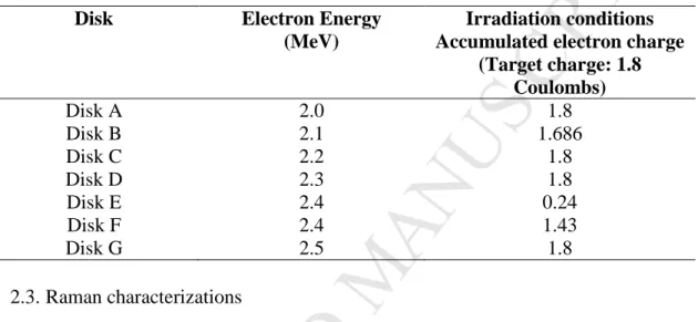
For this study, a 1.8 Coulomb electron charge was initially aimed for the different electron beam energies, but it was difficult to replicate the targeted electron charge for all the irradiation campaigns. The latter was due to technical constraints related to the functioning of the accelerator. Table 1 summarizes the different experimental parameters that were achieved during the UO2 irradiation study.
Table 1: Summary of the electron irradiation parameters that were achieved for the different UO2 disks
Disk Electron Energy (MeV)
Irradiation conditions Accumulated electron charge
(Target charge: 1.8 Coulombs) Disk A 2.0 1.8 Disk B 2.1 1.686 Disk C 2.2 1.8 Disk D 2.3 1.8 Disk E 2.4 0.24 Disk F 2.4 1.43 Disk G 2.5 1.8 2.3.Raman characterizations
The Raman measurements of the virgin and irradiated UO2 disks were carried out using
a Renishaw Invia Reflex confocal spectrometer at the “Conditions Extrêmes et Matériaux: Haute Température & Irradiation” (CEMHTI) Laboratory, Orléans, France. The spectrometer was equipped with a 632.8 nm excitation laser and a holographic grating of 1800 grooves/mm for a spectral acquisition between 400 and 700 cm-1. These
configurations were sufficient to allow a 2-3 cm-1 spectral resolution.
As the intensity of the only Raman-active T2g mode depends on crystallographic
orientation, an ex situ Raman mapping of the virgin and irradiated surfaces was carried out to select the UO2 grains with the maximum Raman intensity, with (100) planes
closely parallel to the surface sample. For such orientation, the Raman intensity will depend on the polarization conditions in the following way: in VV configuration (parallel polarizations for incident and scattered light), the intensity is maximum when
M
AN
US
CR
IP
T
AC
CE
PT
ED
polarization is along [011] axis, and in crossed polarizations (VH), the intensity is maximum for polarizations along fourfold axes (V along [010] and H along [001], and equivalents). Our experimental device is mainly of the VV type configuration.
2.4.PAS analysis
Depth-resolved Doppler Broadening Positron Annihilation Spectroscopy (DB-PAS) was performed using a slow positron beam at CEMHTI-CNRS, France [18]. This spectroscopy is specifically useful to investigate open-volume defects in materials in the near-surface region. Due to its positive charge, positron can be trapped into nucleus depleted region, i.e., neutral or negatively charged open volume defects. The positron annihilates with an electron by producing two gamma rays at around 511 keV whose energy depends on the energy of the electron-positron pair due to the Doppler effect. Thus, the Doppler Broadening spectroscopy allows the measurements of the positron-electron momentum distribution in samples. The shape of the broadened Doppler spectrum is interpreted in terms of shape parameters called S and W. The low momentum parameter (S) corresponds to the fraction of annihilations taking place in the low momentum range (|-2.177| to |2.177|) ×10-3 m0c mainly due to annihilations with
valence electrons. The high-momentum parameter (W) corresponds to the fraction of annihilations taking place in the high momentum range (|-24.88| to |-9.64| and |9.64| to |24.88|) ×10-3 m0c mainly due to annihilations with core electrons. The presence of
vacancy-type defects in a sample compared to a defect-free sample leads to an increase of the S value and a decrease of the W value.
In this study, the average S and W values were measured with a positron beam energy ranging from 16 to 18 keV, i.e., at a mean positron implantation depth of 450-500 nm to avoid any surface effect (oxidation, polishing defects…). Approximately 8×10⁵ events
M
AN
US
CR
IP
T
AC
CE
PT
ED
were collected in the Doppler peak at each positron energy value to ensure a statistical error of 0.11% and 0.26% for S and W values respectively. The S and W values measured in the samples were respectively divided by SL = 0.3713 and WL = 0.07856
values measured in a reference UO2 defect-free sample obtained after annealing at
1700°C during 24 hours in Ar/H2 atmosphere [19].
3.Results
3.1.Raman spectra analysis
The Raman measurements of the UO2 surfaces initially irradiated at 2.0 MeV (1.8 C),
2.1 MeV (1.686 C), 2.2 MeV (1.8 C), 2.3 MeV (1.8 C), 2.4 MeV (1.43 C) and 2.5 MeV (1.8 C) were conducted to study the intensity of the Raman triplet defect bands as a function of electron energy. The electrons also irradiate the UO2 back surfaces with
~500 keV less than their initial energy. Thus, the Raman characterization of the irradiated back surfaces provided relevant information for low energy electrons, namely: 1.5 MeV (1.8 C), 1.6 MeV (1.686 C), 1.7 MeV (1.8 C), 1.8 MeV (1.8 C) and 1.9 MeV (1.43 C) respectively. Figure 1 shows the Raman spectra obtained following the surface analysis of a virgin UO2 disk and the electron-irradiated front and back UO2
surfaces.
[Figure 1 about here.]
The spectrum of the virgin UO2 indicates the presence of the only Raman active T2g
mode occurring at 445 cm-1. The latter is referred to as the symmetry Raman-allowed
phonon scattering of UO2 and is the signature of compounds exhibiting the Fm-3m
space group[20, 21, 22]. The absence of other noticeable peaks suggests that the UO2
M
AN
US
CR
IP
T
AC
CE
PT
ED
Figure 1 shows that electron irradiation induces the apparition of the Raman triplet defect bands in the 500-700 cm-1 spectral range, denoted by U1 (~532 cm-1), U2 (~574
cm-1) and U3 (~636 cm-1). First of all, these spectra look rather similar to those
previously obtained under ionic irradiation [10, 11]. The T2g mode looks only slightly
affected and the three defect lines occur. The spectra for the irradiated disks shown in Figure 1 are very different from what would be obtained on a strongly disordered lattice, where the Raman response would be a VDOS (vibrational density of states)-dominated one. The UO2 VDOS, as reported by Dolling et al. [24], displays a small
peak at the T2g frequency emerging from a broad continuum, that implies a T2g Raman
response much more affected (intensity decrease and broadening) that seen here in Figure 1. This means that the system keeps a crystalline type order.
The intensity of the defect peaks increases as a function of electron energy and is consistent with the increase defects concentration in the UO2 samples. However, the
intensity increase observed in this study is less prominent compared to data reported for alpha and heavy-ion irradiation [10, 11, 25]. Though the Raman defect bands appear clearly for the 2.5 MeV irradiated disk, it is difficult to estimate the electron energy threshold for the defect peaks from Figure 1. A data analysis strategy was adopted to extract the relative intensities of the U1, U2 and U3 peaks as a function of electron energy.
The methodology consisted of an initial baseline subtraction of the raw Raman data to eliminate residual fluorescence signals and background noises. The value of the T2g
peak intensity (T2gMAX) after the baseline subtraction was then recorded. The 510-698
cm-1 spectral range was selected and normalized by the T2gMAX value. These procedures
were applied to each of the acquired spectra. Finally, the Raman spectra of the irradiated disks were subtracted with a reference virgin UO2 spectrum to reveal the
irradiation-M
AN
US
CR
IP
T
AC
CE
PT
ED
induced modifications on the Raman spectra. The main source of error in our approach resides on the removal of background noises, and according to Lewis et al. [26], a relative error of 10% needs to be considered based on the signal to noise ratio following the initial baseline subtraction.
Figure 2 illustrates the irradiation effects on the UO2 Raman spectra in the 509-698 cm-1
spectral range.
[Figure 2 about here.]
As it can be evidenced in Figure 2, the intensity of the Raman triplet defect bands appears very low for electron energy less than 2.0 MeV. However, the triplet defect peaks become prominent as the electron energy is further increased and are seen to occur at 532 cm-1, 574 cm-1, and 636 cm-1 respectively. A classical line fitting
procedure, previously proposed by Guimbretière et al. [14], was carried out by fixing the positions of the defect bands. The intensity values for the three peaks at different electron energies were extracted and are shown in Figure 3.
[Figure 3 about here.]
The figure indicates that the U1, U2 & U3 bands follow a similar behavior under irradiation. It can also be observed that the Raman triplet defect bands do not appear with our error bars below 1.8 MeV, but they show a gradual increase in the 1.9-2.5 MeV electron range.
3.2.PAS characterizations
DB-PAS measurements were initially conducted on the surfaces of the virgin UO2 disk
M
AN
US
CR
IP
T
AC
CE
PT
ED
that a UO2 previously annealed at 1700°C for 24 hours under Ar/H2 reducing
environment is considered as a reference “defect-free” UO2 lattice (referred to as “UO2
Lattice”) for the PAS measurements at CEMHTI-CNRS [19]. The obtained findings for the UO2 Bulk and the reference UO2 Lattice were compared to account for the effect of
annealing temperatures.
The front and back surfaces of the UO2 disks irradiated at 2.1 MeV (1.686 C), 2.2 MeV
(1.8 C) and 2.4 MeV (1.43 C) were characterized. Measurements were also performed on the disk irradiated at 2.4 MeV (0.24 C) to investigate the effect of electron charge on the irradiation-induced defect concentrations. Unfortunately, the disks irradiated at 2.0 MeV, 2.3 MeV and 2.5 MeV were not available for PAS characterizations. The evolution of the (S vs. W) annihilation parameters is shown in Figure 4.
[Figure 4 about here.]
Figure 4 shows that the S(W) values for the different electron energies form a straight line, also referred to as the De-line, with the UO2 Lattice point. This observation
indicates that the same defect-type is formed during the electron irradiation and characterized by the PAS method, but only its concentration varies. The slope of the line (De= 0.60) is very close to the one found by Barthe et al. [19]. The authors carried
out a detailed analysis of UO2 samples irradiated at 1.0 and 2.0 MeV electron energy
with different accumulated electron charges. No defects were detected by PAS for the 1.0 MeV electron irradiation leading to the conclusion that oxygen monovacancy (VO) are positively charged preventing positron trapping into these defects. For the 2.0 MeV electron irradiation, the S(W) values were aligned on the De-line indicating the presence of neutral or negatively charged vacancy-type defects resulting from displacements in the uranium sub-lattice. They suggested that the defects could be uranium
mono-M
AN
US
CR
IP
T
AC
CE
PT
ED
vacancy (VU) or vacancy complexes including VU like U-O di-vacancy or Schottky defect. Recent calculations by Wiktor et al. [27] on the positron lifetime measurements in UO2 showed that the De-line corresponds to a neutral complex defect, made of one
uranium vacancy and two oxygen vacancies, which is referred to as Schottky defects.
From Figure 4, the S(W) point for the virgin UO2 Bulk lies on the Schottky De-line but
away from the reference UO2 Lattice point. This indicates the presence of intrinsic
defects in the virgin UO2 samples used in this study and can be attributed to the lower
annealing temperature (1400°C) employed compared to the defect-free UO2 lattice
(1700°C). Guimbrètiere et al. [14] evidenced a grain boundary Raman signal at 555 cm
-1
for UO2 ceramics annealed at 1700°C. A lower annealing temperature was used in this
study to avoid significant contribution of the grain boundary signal because it occurs in the same spectral range as the irradiation-induced Raman bands. However, the concentration of intrinsic defects in the virgin samples can be considered to be very low because the UO2 Bulk point appears relatively close to the reference UO2 Lattice
point. Let us underline here that in PAS measurements, the analyzed zone is macroscopic compared to the size of grains, and the PAS response integrates contributions of grain cores and grain boundaries, and is then completely dominated by the cores, due to the core/boundary relative surfaces.
In regards to the irradiated samples, electron irradiation causes a gradual shift of the S(W) points from the UO2 Lattice, thus indicating that Schottky-type defects are created
under all irradiation conditions. The concentration of defects can be seen to depend on electron energy. The effect of electron charge can be observed by considering the UO2
disks irradiated at 2.4 MeV with a low (0.24 C) and high (1.43 C) charge. Figure 4 shows that the shift of the S(W) point relative to the reference UO2 Lattice point is more
M
AN
US
CR
IP
T
AC
CE
PT
ED
important for the high electron charge and hence confirms that the concentration of Schottky defects also depends on the electron charge.
4.Discussion
In this section, a detailed interpretation of the experimental findings is carried out to investigate the origin of the Raman triplet defect bands. An attempt is then made to identify the defect types responsible for the apparition of the irradiation-induced Raman peaks.
4.1.Attribution of the Raman triplet defect bands to nuclear or electronic stopping power
The experimental results revealed that the irradiation-induced Raman bands behave identically under irradiation. It was also evidenced that the concentration of defects depends on the electron charge. The overall change in the defect band intensity (U1+U2+U3) for the different electron irradiations that were achieved with a sufficiently high electron charge (1.43-1.8 C) was only considered for the data interpretation. The obtained findings are presented in Figure 5.
[Figure 5 about here.]
The intensity of the Raman defect bands remains negligible below 1.8 MeV but then increases almost linearly when the electron energy is increased up to 2.5 MeV. The figure also shows that the electron energy threshold for the apparition of the Raman defect bands can be estimated to be between 1.8-1.9 MeV.
The ESTAR program code [16] and the Non-Ionizing Energy Loss (NIEL) calculator [17] were used to determine the values of the electronic and nuclear stopping of the electrons in UO2. These theoretical values were required to investigate the origin of the
M
AN
US
CR
IP
T
AC
CE
PT
ED
Raman defect bands. The calculated electronic and nuclear stopping powers, in the 1.0-2.5 MeV electron energy range, are illustrated in Figure 6.
[Figure 6 about here.]
From Figure 5 and Figure 6, the intensity of the Raman defect bands is observed to follow a similar trend as the nuclear stopping power; both do not display significant evolution below 1.5 MeV but are characterized by a continuous increase between 1.8 MeV and 2.5 MeV. On the contrary, the energy loss due to the inelastic collisions of the electrons with the U and O atoms remains almost constant over the entire electron energy range. These results suggest that the irradiation-induced bands observed on the Raman spectra of irradiated UO2 take their origin from the elastic collisions of incident
electrons with U and O atoms and are due to the formation of atomistic defects.
4.2.Attribution of the Raman triplet defect bands to the defect types resulting from the elastic collisions
Electron irradiation can induce atomic defects given that the energy of the incident electrons is high enough to displace atoms from their normal positions in the crystal lattice. As previously reported in this study, PAS measurements confirmed the presence of point defects in the irradiated disks. The concentration of displaced atoms was also observed to depend on electron energy and irradiation charge. In regards to Raman spectroscopy, the increase of the defect bands intensity in the ballistic regime indicates that they are consistent with atomistic defects. This study was extended to identify the defect types that induce the apparition of the Raman triplet defect bands, i.e., to differentiate between uranium and oxygen defects.
The concentration of uranium and oxygen point defects were calculated using differential cross-section values for displacements in the UO2 lattice as reported by
M
AN
US
CR
IP
T
AC
CE
PT
ED
Soullard [28]. The calculated point defect concentrations as a function of electron energy are presented in Figure 7.
[Figure 7 about here.]
Figure 7 shows that electrons with energy greater than 1.6 MeV are required to induce displacements in the uranium sub-lattice. The concentration of uranium defects can also be observed to depend on electron energy. According to Soullard [28], electron energies as low as 0.5 MeV are sufficient to displace oxygen atoms, but their concentration remains unchanged between 1.4 MeV and 2.5 MeV.
The increase in the uranium defect concentration, observed between 1.8 MeV and 2.5 MeV, is consistent with the evolution of the Raman triplet defect bands in the same energy range (Figure 5). These results indicate that the irradiation-induced Raman bands are linked to uranium-type point defects, but through an indirect mechanism; the defects lower the local symmetry, giving rise to new allowed modes in a lower symmetry group. But these new modes are dominated by oxygen vibrations, due to their frequency range. The Raman data are also supported by PAS measurements which showed the presence of Schottky defects, i.e., point defects involving uranium vacancies, in the irradiated UO2 samples. The good agreement between the DB-PAS S-parameter and the
intensity of the Raman triplet defect bands for the same electron energy and irradiation charge can be evidenced in Figure 8. The latter reveals that both methods characterize defects resulting from displacements in the uranium sub-lattice.
[Figure 8 about here.]
However, a slight variance in the electron energy threshold for the apparition of the Raman triplet defect bands and the PAS (E) parameter can be observed in Figure 8. The
M
AN
US
CR
IP
T
AC
CE
PT
ED
minimum electron energy required to induce the Raman triplet bands lies between 1.8 MeV and 1.9 MeV. On the other hand, PAS method can characterize point defects that are generated by electrons with energy close to 1.6 MeV. The difference in the electron energy threshold can be attributed to the much higher sensitivity of the PAS to characterize defects compared to Raman spectroscopy.
4.3.Raman triplet defect bands: Uranium interstitials vs. Uranium vacancies
The electron irradiation experiment allowed to assign the Raman defect bands to irradiation damages involving uranium-type point defects. However, additional information is still required to differentiate between uranium interstitials and uranium vacancies. The Raman and PAS data available in the literature were considered to determine the exact origin of the Raman defect bands.
Labrim et al. [29] investigated the thermal evolution of the S and W annihilation parameters of a 45 MeV alpha-irradiated UO2 disk. The authors reported that the PAS
signals, which are relevant to uranium vacancy-related defects, are annealed at temperatures between 800°C and 1300°C. These data are in good agreement with studies carried out by Nakae et al. [30] and Weber [31]. On the other hand, Desgranges et al. [32] studied the annealing behavior of the Raman triplet defect peaks under high-temperature conditions and showed that the defect bands induced by a 25 MeV alpha beam are annealed between 375°C and 525°C.
The difference in the annealing temperatures indicates that these two methods characterize different types of uranium defects. In this study, the presence of irradiation-induced Schottky defects was confirmed by PAS due to the annihilation of positrons in negatively charged uranium vacancy sites (which is not the case for oxygen vacancies). PAS is predominantly sensitive to vacancy-type defects; thus, it can be stipulated that
M
AN
US
CR
IP
T
AC
CE
PT
ED
the Raman triplet defect bands are due to a complex defect that involves uranium interstitials.
In this study, it was observed that electron irradiation induces a relatively low concentration of point defects. It is therefore unlikely that the new chemical bonds they generate are at the origin of the triplet defect bands. However, each point defect can cause a re-arrangement of the atoms which surround or are located near the defect. This results in a slight displacement of these atoms from their original positions and gives rise to a domain with a specific symmetry which is different from that of the Fm-3m prevailing in UO2. It is most likely that these domains have a symmetry lower than
Fm-3m with the loss of one or more symmetry elements, such as translational symmetry, centering F or a symmetry operation, like for instance mirror or rotation operations and is responsible for the apparition of the Raman triplet defect bands. A study is currently underway to determine the loss of which element of symmetry could be at the origin of the appearance of the defect bands.
5.Conclusions
This study was devoted to provide an in-depth analysis of the triplet defect bands that appear on the Raman spectra of irradiated nuclear fuels. An experiment was performed whereby several sintered UO2 disks were irradiated with electrons of different energies
and were then subjected to ex situ Raman and PAS measurements.
Experimental results showed that the electron energy threshold for the apparition of the Raman triplet defect bands lies between 1.8-1.9 MeV, beyond which the intensity of the defect bands exhibits a continuous increase up to 2.5 MeV. This observation is in good agreement with the evolution of the nuclear stopping power in the same energy range
M
AN
US
CR
IP
T
AC
CE
PT
ED
and implies that the Raman defect bands are due to the formation of atomistic defects resulting from the ballistic collisions of the incident electrons with U and O atoms.
A detailed Raman analysis coupled with PAS measurements showed that the Raman bands occur due to displacements in the uranium sub-lattice. These point defects induce the re-arrangement of UO2 lattice atoms giving rise to domains with a specific
symmetry which is different from that of the Fm-3m prevailing in UO2.
6.Acknowledgements
This work was conducted and funded within the framework of the French Tripartite Institute CEA/EDF/Framatome [Project Transport et Entreposage]. The authors are grateful to the EMIR committee for allocating LSI beamtime. C. Tanguy and D. Drouan (CEA/DEN/LLCC) are warmly acknowledged for their assistance with samples preparations.
7.Data availability
The raw/processed data that support the findings of this study are available from the corresponding author, [R. Mohun], upon request.
8.References
[1] C. Sabathier, G. Martin, A. Michel, G. Carlot, S. Maillard, C. Bachelet, F. Fortuna, O. Kaitasov, E. Oliviero and P. Garcia, "In-situ TEM observation of nano-void formation in UO2 under irradiation," Nucl. Instrum. Methods B., vol. 326, p. 247–
250, 2014.
[2] H. Palancher, R. Kachnaoui, G. Martin, A. Richard, J. Richaud, C. Onofri, R. Belin, A. Boulle, H. Rouquette, C. Sabathier, G. Carlot, P. Desgardin, T. Sauvage, F. Rieutord, J. Raynal, P. Goudeau and A. Ambard, "Strain relaxation in He implanted UO2 polycrystals under thermal treatment: An in situ XRD study," J.
M
AN
US
CR
IP
T
AC
CE
PT
ED
[3] H. Chiang, T. Zweifel, H. Palancher, A. Bonnin, L. Beck, P. Weiser, M. Döblinger, C. Sabathier, R. Jungwirth and W. Petry, "Evidence of amorphous interdiffusion layer in heavy ion irradiated U-8wt%Mo/Al interfaces," J. Nucl. Mat., vol. 440, p. 117–123, 2013.
[4] G. Carlot, C. Sabathier, S. Maillard, A. Michel, G. Martin, E. Gilabert, F. Fortuna and P. Garcia, "Study of Rare Gases Behavior in Uranium Dioxide," in EPJ Web of
Conferences, INSTN Cadarache, France, 2016.
[5] J. Crocombette, L. Van Brutzel, D. Simeone and L. Luneville, "Molecular dynamics simulations of high energy cascade in ordered alloys: Defect production and subcascade division," J. Nucl. Mat., vol. 474, p. 134–142, 2016.
[6] S. Maillard, G. Martin and C. Sabathier, "Why a steady state void size distribution in irradiated UO2? A modeling approach.," Nucl. Instrum. Methods B., vol. 374, p.
58–66, 2016.
[7] G. Martin, P. Garcia, C. Sabathier, F. Devynck, M. Krack and S. Maillard, "A thermal modelling of displacement cascades in uranium dioxide," Nucl. Instrum.
Methods B., vol. 327, p. 108–112, 2014.
[8] G. Martin, P. Garcia, C. Sabathier, L. Van Brutzel, B. Dorado, F. Garrido and S. Maillard, "Irradiation-induced heterogeneous nucleation in uranium dioxide," Phy.
Let. A, vol. 374, p. 3038–3041, 2010.
[9] R. Skorek, S. Maillard, A. Michel, G. Carlot, E. Gilabert and T. Jourdan, "Modelling Fission Gas Bubble Distribution in UO2," Defect and Diffusion Forum,
Vols. 323-325, p. 209–214, 2012.
[10] C. Onofri, C. Sabathier, H. Palancher, C. Carlot, S. Miro, Y. Serruys, L. Desgranges and M. Legros, "Evolution of extended defects in polycrystalline UO2
under heavy ion irradiation: combined TEM, XRD and Raman study," Nucl.
Instrum. Methods B., vol. 374, pp. 51-57, 2016.
[11] R. Mohun, L. Desgranges, J. Léchelle, P. Simon, G. Guimbretière, A. Canizarès, F. Duval, C. Jégou, M. Magnin, N. Clavier, N. Dacheux, C. Valot and R. Vauchy, "Charged defects during alpha-irradiation of actinide oxides as revealed by Raman and luminescence spectroscopy," Nucl. Instrum. Methods B., vol. 374, pp. 67-70, 2016.
[12] Z. Talip, T. Wiss, P. Raison, J. Paillier, D. Manara, J. Somers and R. Konings, "Raman and X‐ray Studies of Uranium–Lanthanum‐Mixed Oxides Before and After Air Oxidation," J. Am. Ceram. Soc., vol. 98, pp. 2278-2285, 2015.
M
AN
US
CR
IP
T
AC
CE
PT
ED
and Electrochemical Properties of Uranium Dioxide (UO2)," J. Electrochem. Soc.,
vol. 161, pp. H105-H113, 2014.
[14] G. Guimbretière, L. Desgranges, A. Canizarès, G. Carlot, R. Caraballo, C. Jégou, F. Duval, N. Raimboux, M. Ammar and P. Simon, "Determination of in-depth damaged profile by Raman line scan in a pre-cut He2+ irradiated UO2," Appl. Phys.
Lett., vol. 100, p. 251914, 2012.
[15] O. Maslova, G. Guimbretière, M. Ammar, L. Desgranges, C. Jégou, A. Canizarès and P. Simon, "Raman imaging and principal component analysis-based data processing on uranium oxide ceramics," Mat. Characterization, vol. 129, pp. 260-269, 2017.
[16] M. Berger, J. Coursey, M. Zucker and J. Chang, "ESTAR: Stopping powers and ranges for electrons calculator," National Institute of Standards and Technology , [Online]. Available: https://physics.nist.gov/PhysRefData/Star/Text/ESTAR.html. [Accessed 24 September 2017].
[17] M. Boschini, P. Rancoita and M. Tacconi, "SR-NIEL Calculator: Screened Relativistic (SR) Treatment for Calculating the Displacement Damage and Nuclear Stopping Powers for Electrons, Protons, Light- and Heavy- Ions in Materials (version 3.9.5)," INFN sez. Milano-Bicocca, Italy, 2014. [Online]. Available: http://www.sr-niel.org/index.php/electrons-niel-calculator. [Accessed 10 August 2017].
[18] P. Desgardin, L. Liszkay, M. Barthe, L. Henry, J. Briaud, M. Saillard, L. Lepolotec, C. Corbel, G. Blondiaux, A. Colder, P. Marie and M. Levalois, "Slow Positron Beam Facility in Orléans," Mat. Sci. Forum, Vols. 363-365, pp. 523-525, 2001.
[19] M. Barthe, H. Labrim, A. Gentills, P. Desgardin, C. Corbel, S. Esnouf and P. Piron, "Positron annihilation characteristics in UO2: for lattice and vacancy defects
induced by electron irradiation," Phys. Stat. Sol., vol. 10, pp. 3627-3632, 2007. [20] P. Graves, "Raman microprobe spectroscopy of uranium dioxide single crystals and
ion implanted polycrystals," Appl. Spectrosc., vol. 44, pp. 1665-1667, 1990.
[21] G. Allen, I. Butler and N. Tuan, "Characterization of uranium oxides by micro-Raman spectroscopy," J. Nucl. Mat., vol. 144, pp. 17-19, 1987.
[22] D. Manara and B. Renker, "Raman spectra of stoichiometric and hyper-stoichiometric uranium dioxide," J. Nucl. Mat., vol. 321, p. 233–237, 2003.
[23] L. Desgranges, G. Baldinozzi, P. Simon, G. Guimbretière and A. Canizarès, "Raman spectrum of U4O9: a new interpretation of damage lines in UO2," J.
M
AN
US
CR
IP
T
AC
CE
PT
ED
Raman Spec., vol. 43, pp. 455-458, 2012.
[24] G. Dolling, R. Cowley and A. Woods, "The Crystal Dynamics of Uranium Dioxide," Canadian Journal of Physics, vol. 43(8), pp. 1397-1413, 1965.
[25] G. Guimbretière, L. Desgranges, A. Canizarès, R. Caraballo, F. Duval, N. Raimboux, R. Omnée, M. Ammar, C. Jégou and P. Simon, "In situ Raman monitoring of He2+ irradiation induced damage in a UO2 ceramic," Appl. Phys.
Lett., vol. 103, p. 041904, 2013.
[26] I. Lewis and H. Edwards, Handbook of Raman Spectroscopy: From the Research Laboratory to the Process Line, New York : Marcel Dekker, Inc. , 2001.
[27] J. Wiktor, "Coupled experimental and DFT+U investigation of positron lifetimes in UO2," PhD thesis, Aix-Marseille University, 2015.
[28] J. Soullard, "High voltage electron microscope observations of UO2," J. Nucl. Mat.,
vol. 315, pp. 190-196, 1985.
[29] H. Labrim, M. Barthe, P. Desgradin, T. Sauvage, C. Corbel, G. Blondiaux and J. Piron, "Thermal evolution of the vacancy defects distribution in 1 MeV helium implanted sintered UO2," Nucl. Instrum. Methods B., vol. 261, p. 883–887, 2007.
[30] N. Nakae, Y. Iwata and T. Kirihara, "Thermal recovery of defects in neutron irradiated UO2," J. Nucl. Mat., vol. 80, pp. 314-322, 1979.
[31] W. Weber, "Thermal recovery of lattice defects in alpha-irradiated UO2 crystals,"
J. Nucl. Mat., vol. 114, pp. 213-221, 1983.
[32] L. Desgranges, G. Guimbretière, P. Simon, F. Duval, R. Omnée, C. Jégou and R. Caraballo, "Annealing of the defects observed by Raman spectroscopy in UO2
irradiated by 25 MeV He2+ ions," Nucl. Instrum. Methods B., vol. 327, p. 74–77, 2014.
M
AN
US
CR
IP
T
AC
CE
PT
ED
Raman spectra of a virgin UO2 and the disks irradiated at different electron energy. Results shown
here were obtained following the Raman mapping of UO2 surfaces using the Renishaw Invia
spectrometer with the parameters indicated in the text. The Raman spectra were then normalized by the T2g peak intensity.
M
AN
US
CR
IP
T
AC
CE
PT
ED
Evolution of the irradiation-induced Raman signals as a function of electron energy in the 509-698 cm-1 spectral range. These results were obtained by subtracting the Raman spectra of irradiated samples with a reference virgin UO2 spectrum after the initial baseline subtraction followed by the
data normalization step. (For interpretations of the references to color in this figure, the reader is referred to the online version of this manuscript).
M
AN
US
CR
IP
T
AC
CE
PT
ED
Evolution of U1 (532 cm-1), U2 (574 cm-1) & U3 (636 cm-1) as a function of electron energy. Findings shown here were obtained from the line fitting procedure by fixing the positions of the defect bands. (For interpretations of the references to color in this figure, the reader is referred to the online version
M
AN
US
CR
IP
T
AC
CE
PT
ED
Relative low momentum fraction S/SL versus relative high momentum fraction W/WL for the virgin
and electron-irradiated UO2. Measurements were performed using a positron beam energy ranging
from 16 to 18 keV and the obtained S and W data were then divided by reference values (SL = 0.3713
and WL = 0.07856) corresponding to a defect-free UO2 lattice. (For interpretations of the references to
M
AN
US
CR
IP
T
AC
CE
PT
ED
Overall evolution of the Raman triplet bands intensity (U1+ U2+ U3) as a function of electron energy for the irradiation charge between 1.43 C-1.8 C
M
AN
US
CR
IP
T
AC
CE
PT
ED
Electronic and nuclear stopping power for electrons (1.0-2.5 MeV energy range) in UO2. Simulations
were performed using the ESTAR code (electronic stopping power) and the NIEL program code (nuclear stopping power). For the calculations, the displacement energy (Ed) of oxygen and uranium
M
AN
US
CR
IP
T
AC
CE
PT
ED
The uranium and oxygen point defects concentration in the 1.4-2.5 MeV electron energy range. Calculations were performed using the irradiation parameters for the considered electron energies and
M
AN
US
CR
IP
T
AC
CE
PT
ED
Comparison of the PAS (S/SL) and Raman (U1 + U2 + U3) results in the 1.6-2.5 MeV electron energy