HAL Id: hal-01887151
https://hal.archives-ouvertes.fr/hal-01887151
Submitted on 18 Oct 2018
HAL is a multi-disciplinary open access
archive for the deposit and dissemination of
sci-entific research documents, whether they are
pub-lished or not. The documents may come from
teaching and research institutions in France or
abroad, or from public or private research centers.
L’archive ouverte pluridisciplinaire HAL, est
destinée au dépôt et à la diffusion de documents
scientifiques de niveau recherche, publiés ou non,
émanant des établissements d’enseignement et de
recherche français ou étrangers, des laboratoires
publics ou privés.
H. Bohuslavskyi, S. Barraud, V. Barral, M. Cassé, L. Le Guevel, L. Hutin, B.
Bertrand, A. Crippa, X. Jehl, Gaël Pillonnet, et al.
To cite this version:
H. Bohuslavskyi, S. Barraud, V. Barral, M. Cassé, L. Le Guevel, et al.. Cryogenic Characterization
of 28-nm FD-SOI Ring Oscillators With Energy Efficiency Optimization. IEEE Transactions on
Electron Devices, Institute of Electrical and Electronics Engineers, 2018, 65 (9), pp.3682 - 3688.
�10.1109/TED.2018.2859636�. �hal-01887151�
1
Abstract—Extensive electrical characterization of ring oscillators (ROs) made in high-k metal gate 28nm Fully-Depleted Silicon-on-Insulator (FD-SOI) technology is presented for a set of temperatures between 296 and 4.3K. First, delay per stage (P),
static current (ISTAT), and dynamic current (IDYN) are analyzed for
the case of the increase of threshold voltage (VTH) observed at low
temperature. Then, the same analysis is performed by compensating VTH to a constant, temperature independent value
through forward body-biasing (FBB). Energy efficiency optimization is proposed for different supply voltages (VDD) in
order to find an optimal operating point combining both high RO frequencies and low power dissipation. We show that the Energy-Delay product (EDP) can be significantly reduced at low temperature by applying a forward body bias voltage (VFBB). We
demonstrate that outstanding performance of RO in terms of speed (p=37ps) and static power (7nA/stage) can be achieved at
4.3K with VDD reduced down to 0.325V.
Index Terms—Cryogenic electronics, 28nm FD-SOI, ring oscillator, back-biasing, quantum computing, ultra-low-power.
I. INTRODUCTION
ince the famous proposal for quantum computing with quantum dots [1], significant progress in Si spin qubits have been reported [2-5]. The first two-qubit logic gate in isotopically enriched Si was demonstrated [3] and a foundry-compatible CMOS SOI platform was used to demonstrate a hole spin qubit functionality [4-5]. These major achievements on the basic building block of a quantum computer are paving the way to the implementation of a large number of qubits individually controlled with tunable nearest-neighbor couplings. However, scaling up these systems in complex quantum computing architectures can be extremely challenging. In addition to fundamental advances in physical understanding and material development needed for spin qubits, a consistent engineering work should be made to propose a means of controlling, interacting and reading out a large number of qubits in parallel.
In recent years, hardware interfaces based on advanced CMOS technologies that operate at cryogenic temperature so as to ensure proximity to qubits have been proposed and discussed [6-9]. Bulk Si MOSFET [10-13] and other basic circuits such as Ring Oscillators (ROs) [11] and an FPGA (Field-Programmable Gate Array) [14] were characterized down to
H. Bohuslavskyi, S. Barraud, V. Barral, M. Cassé, L. Le Guevel, L. Hutin, G. Pillonnet, B. Bertrand and M. Vinet are with CEA, LETI, Minatec Campus, F-38054 Grenoble, France. X. Jehl, L. Jansen, A. Crippa, R. Maurand, S. De Franceschi, and M. Sanquer are with Univ. Grenoble Alpes, CEA,
INAC-4K. Despite a significant reduction of subthreshold swing (SS) and improvement of carrier mobility at low temperature, some limitations have been raised on bulk Si technologies. Non-ideal kink behavior and hysteresis in the characteristics are induced by the bulk current generated by impact ionization at the drain combined with increased resistivity from the freeze-out of charge carriers [15]. Moreover, the increase of drive current from the enhanced carrier mobility at low temperature is partially mitigated by the increase of threshold voltage which can be hardly compensated by back-biasing in bulk technologies.
In this work, an alternative to bulk Si CMOS technologies is proposed in order to provide more flexibility to designers for optimizing both high-performance and low power cryogenic electronics. Undoped thin-planar 28nm FD-SOI devices offer an excellent short-channel electrostatic control, low leakage current and immunity to random dopant fluctuations. More flexibility is brought to the circuit through an extremely effective back-biasing allowing to switch dynamically between high performance mode (Forward Body Biasing) and ultra-low leakage mode (Reverse Body Biasing) [16]. We thus propose to study the low temperature characterization of 28nm FD-SOI ring oscillators (RO) down to 4.3K. The RO performance in terms of delay per stage (P), dynamic (IDYN), and static (ISTAT)
currents is studied from 296 down to 4.3K for VDD ranging
between 0.325 and 1.2V. Cryogenic effects on the RO performance are investigated with and without forward back-biasing (FBB) in order to compensate the shift of threshold voltage (VTH) at low temperature. In addition, an energy
efficiency optimization using FBB is proposed. We show that VDD can be reduced down to 0.325V while maintaining an
ultra-low Energy-Delay product (EDP).
The paper is organized as follows: a brief review of 28nm FD-SOI is given in Section II. Low temperature characterization of FD-SOI ring oscillators and their energy efficiency optimization are discussed in Section III. Finally, the main conclusions are drawn in Section IV.
II. BRIEF REVIEW OF 28NM FD-SOI TECHNOLOGY
The GO1 FD-SOI transistors are fabricated with a gate-first high-metal gate using STMicroelectronics technology [17-18]. They are processed on 300mm (100) SOI wafers with a buried oxide (BOX) thickness of 25nm. The equivalent oxide
PHELIQS, F-38054 Grenoble, France. F. Arnaud and P. Galy are with STMicroelectronics, 850 rue J. Monnet, 38920 Crolles, France.
E-mail: [email protected]
Cryogenic characterization of 28nm FD-SOI ring
oscillators with energy efficiency optimization
H. Bohuslavskyi, S. Barraud, V. Barral, M. Cassé, L. Le Guevel, L. Hutin, B. Bertrand, A. Crippa, X. Jehl,
G. Pillonnet, A.G.M. Jansen, F. Arnaud, P. Galy, R. Maurand, S. De Franceschi, M. Sanquer, and M. Vinet
architecture: N-well (resp. P-well) with p-type (resp. n-type) back-plane doping for n-MOS (resp. p-MOS).
Fig. 1. (a) Schematic layout of 101-stages ring oscillator with 1024-frequency divider (FD). (b) Single inverter stage composed of n- and p-MOS. (c) Illustration of LVT transistors in the flip-well configuration. VCC is the supply
voltage of the clock divider polarized with +1V. VENB controls the AND gate
that enables the oscillations (VENB=VDD was kept during all the measurements).
For more details on the measurement protocol, see Table I. TABLEI
RING OSCILLATOR AND MOSFET PARAMETERS, UNITS, DESCRIPTION, AND MEASUREMENT PROTOCOL
Parameter Unit Description Measurement protocol f Hz RO frequency VENB=VDD, VCC =1V and
measure OUT. P ps RO delay per stage = 1/(f21011024). IDYN A/ stage Dynamic current per stage in oscillating state VENB=VDD, VCC =GND and measure OUT. ISTAT nA/ stage
Static current per stage in non-oscillating state VENB = VCC =GND and measure OUT. IEFF A Effective drive current of FD-SOI transistor [19]
IEFF = 1/(1/ IEFF-N + 1/ IEFF-P)
IEFF-N(P) = (IH+ IL)/2 where
IH =IDS (VGS =VDD,
VD =VDD/2)
IL =IDS (VGS =VDD/2,
VD =VDD)
where VGS, VDS, and IDS are
MOSFET gate voltage, drain voltage and drain current.
G(IEFF) % IEFF enhancement at low temperature EFF (T) - EFF (296K)] / EFF (T) G(P) % P enhancement at low temperature P (T) - P (296K)] /P (T) EPT fJ Energy per
transition
=101P (IDYN - ISTAT)
VDD EDP fJps Energy Delay
product = P EPT
A 34nm gate length (LG) is considered for both n- and p-MOS
transistors of width WNMOS=420nm and WPMOS=600nm.The
schematic layout of RO in the flip-well configuration is shown
frequency divider to lower its frequency in the sub-MHz regime. The parameters and the measurement protocols used in this work are summarized in Table I.
III. RESULTS AND DISCUSSION
A. RO performance at room temperature
In contrast to usual bulk technology, ultra-thin body and buried oxide FD-SOI enables an extended body-bias range from -3V (RBB) up to +3V (FBB), thanks to the thin buried oxide providing either high-performance or low-power transistors [20]. In order to compensate the increase of VTH at
low-temperature this work is focused on LVT transistors which enable a strong improvement in the switching speed thanks to FBB (body factor of 85mV/V) at the cost of a higher leakage current. When no input is provided on the AND logic gate, ISTAT
and then static power consumption occur due to the flow of leakage from supply to ground. For the room temperature data in Fig. 2, the static current of 101-stages RO is plotted as a function of the delay per stage for different VDD and FBB
voltages (VFBB). Let us note that the delay of CMOS invertor
can be approximated by P = CLOAD×VDD/IEFF [21] with IEFF the
effective current (defined in Table I) and CLOAD the load
capacitance including the inversion capacitance, the parasitic capacitances and the wiring capacitance of back-end-of-line. Hence, lowering the supply voltage VDD to achieve lower static
power dissipation (i.e. lower ISTAT) degrades the RO
performance giving higher delay per stage. This frequency reduction can be balanced by using FBB voltage. The efficiency of forward back biasing for P reduction and improved
performance is well observed in Fig. 2. For the RO operating at VDD=1V, a p reduction of 33% is achieved (at VFBB=2.8V) at
the expense of a significant enhancement of static current (i.e. static power dissipation). Thus, a compromise in terms of power dissipation and speed should be carefully considered. Maintaining the back biasing efficiency at very low temperature is crucial to ensure accuracy and speed in the control and readout of qubits while using comparatively less power dissipation to perform the calculations.
Fig. 2. Static current vs delay per stage for a set of VDD from 0.7 to 1.2V
(VDD=50mV). Three different FBB voltages are considered. ISTAT is
significantly increased at high VFBB illustrating that ROs are well optimized at
room temperature with VFBB=0V.
IV-1 IV-2 IV-101
VENB FD /1024 OUT GND VDD VN-WELL VCC VP-WELL GND VDD VIN VOUT NMOS PMOS VP-WELL VN-WELL S D PMOS NMOS N-well P-well p-type back-plane N+ P+
SiO2 SiO2 SiO2
S D
a)
b)
c)
LVT Ring Oscillator LG = 34nm WNMOS = 420nm WPMOS = 600nm n-type back-plane BOX BOX3
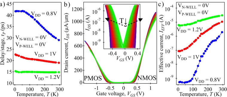
Fig. 3. (a) Delay per stage vs temperature for VDD =0.8, 1, and 1.2V showing the RO slowing down due to the increase of VTH at low temperature. (b) IDS -VGS
curves recorded at VDD = 1V plotted in linear scale. The insert shows the subthreshold regime where current is plotted in logarithmic scale. Green (resp. blue) color
corresponds to room temperature (resp. 4.3K). (c) Effective current vs temperature for different VDD. The procedure used to calculate IEFF is described in Table I.
B. RO performance without FBB down to 4.3K Operation of FD-SOI transistors at cryogenic temperature was already reported in [18,22,23]. Since the scattering of charge carriers with phonons is sufficiently weak and can be neglected at liquid helium temperature, electron and hole mobilities are enhanced and should lead to a smaller p at lower
temperature for a given VDD. However, despite a significant
increase of drive current expected at low temperature [18], the RO slows down as it can be seen in Fig. 3a. This increase of delay per stage is explained by the VTH-shift at lower
temperatures (Fig. 3b) for both n- and p-MOS transistors. Consequently, the effective current is strongly reduced at lower temperatures due to a lower overdrive current for the gate voltage. This IEFF reduction becomes especially important at
low VDD. Hence, without FBB (VN-WELL=VP-WELL=0V) the
enhanced carrier mobility at low temperature does not improve the effective current which becomes strongly limited by the VTH
increase. The IEFF reduction shown on Fig. 3c is then directly
responsible for the observed increase of P. The degradation of
RO performance becomes even more important at low VDD.
Therefore, without forward-back-biasing used to compensate the VTH-shift it may be difficult to work with an optimized
cryogenic digital control electronics combining the demands of both high-performance and low-power consumption.
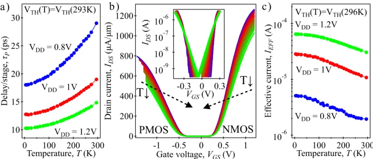
C. RO performance by applying FBB down to 4.3K In order to preserve the benefit of higher carrier mobility and thus, higher driving current at low temperatures, the VTH-shift
should be compensated. The ability to adjust VTH through
back-biasing was already successfully demonstrated down to 4.3K using 28nm FD-SOI transistors [18]. In this work, the threshold voltages of n- and p-MOSFET as well as the body-factors (VTH/VFBB) were systematically extracted over a wide range
of VFBB from 0 up to 3V. Then, by adjusting VN-WELL and V P-WELL for each temperature, the VTH-shift was compensated (in
order to keep the VTH measured at 300K) and thus, VTH_NMOS
and VTH_PMOS were kept constant in temperature as shown in
Fig. 4b. In contrast to previous results (without FBB), a significant speed up for different VDD is now observed when
threshold voltages were settled to VTH(T)=VTH(296K) within
the full temperature range (Fig. 4a). y reducing the temperature from room temperature down to 4.3K, the delay per stage is decreased by 38% at VDD=0.8V, 33% at VDD=1V, and
31% at VDD=1.2V. The P reduction can be explained by the
increase of IEFF shown in Fig. 4c. By monitoring the
enhancement of IEFF and P at lower temperatures (down to
4.3K) we observe a good correlation between the relative variations of IEFF increase and the P reduction for VDD=0.8V as
shown in Fig. 5. Hence, the load capacitance seems to be weakly dependent on temperature since the IEFF increase is
mainly responsible for the speed up of RO at low temperature. Besides the low temperature behavior of P, other critical
parameters such as dynamic current (IDYN) and static current
(ISTAT) were monitored for the evaluation of the power
dissipation in oscillating and sleeping mode. As shown in Fig. 6, IDYN naturally increases as the temperature is reduced
due to the IEFF enhancement, which leads to the increase of
active power dissipation. Indeed, by applying FBB for the VTH
compensation, the effective current is improved due to higher carrier mobility at low temperature and then IDYN is enhanced.
In comparison to the room temperature case, the IDYN
enhancement normalized by VDD is about 34% at 4.3K. At the
same time a significant reduction in static current (Fig. 6b) and thus, in static power dissipation is observed thanks to the decrease of subthreshold slope at low temperature [18].
Fig. 4. (a) Delay per stage vs temperature for VDD =0.8V, 1V, and 1.2V in the case of compensated VTH. The RO speeds up at low temperature due to the carrier
mobility enhancement. (b) IDS-VGS curves recorded at VDD=1V plotted in linear scale. The insert shows the subthreshold behavior with current plotted in logarithmic
scale. VTH_NMOS and VTH_PMOS within the whole temperature range are constant and can be found in Table II. Green (resp. blue) color corresponds to room temperature
(resp. 4.3K) (c) Effective current vs temperature for different VDD. As it can be seen in Fig. 4b, the effective current increases at any stage of cooling down.
As compared to room temperature, the calculated static power dissipation PSTAT=ISTAT×VDD at 4.3K is reduced by a factor of
1600 (VDD=0.8V), 100 (VDD=1V), and 6.5 (VDD=1.2V). The
RO performance in terms of P, IDYN, and ISTAT measuredat 4.3
and 296K with and without FBB are summarized in Table II. D. Energy efficiency optimization down to 4.3K. Wiring up large qubit arrays today is a key issue across all qubit platforms. Indeed, a large number of qubits must be read out periodically and rapidly processed to check whether errors occur along the way and to correct them. Furthermore, the energy efficiency of a cryogenic platform for the classical control of a scalable quantum computer is essential. Low power dissipation is required, down to few watts at 4K [24] to enable
Fig. 5. Relative enhancement of IEFF and p at VDD = 0.8V for temperature
between 296 and 4.3K. FBB is applied to compensate the increase of VTH at low
temperatures. Note that both relative gains are well correlated within the whole
temperature range. Fig. 6. (a) Dynamic current and (b) static current as a function of temperature for different V
DD in case of compensated VTH. Note that ISTAT continuously
decreases and reaches 2.3 pA/stage for VDD=0.8V at 4.3K.
60
50
40
30
20
10
0
G
ai
n
(
%
)
300
250
200
150
100
50
0
Temperature, T (K)
G(τ
P)
G(I
EFF)
V
DD= 0.8V
V
TH(T)=V
TH(296K)
> REPLACE THIS LINE WITH YOUR PAPER IDENTIFICATION NUMBER (DOUBLE-CLICK HERE TO EDIT) < 5
TABLEII
COMPARISON OF RING OSCILLATOR PERFORMANCE AT 296K AND 4.3K
BETWEEN UNCOMPENSATED AND COMPENSATED VTH
T (K) VDD (V) VTH_NMOS (V) VN-WELL (V) P (ps) IDYN
nA/stage) nA/stage) ISTAT
VTH_PMOS (V) VP-WELL (V) 296 0.8 0.224 0 27 497 0.67 -0.376 0 1 0.216 0 18 885 1.29 -0.363 0 1.2 0.208 0 14 1308 1.9 -0.352 0 4.3 0.8 0.391 0 42 363 0.002 -0.549 0 0.224 1.65 18 717 0.002 -0.376 -2.75 1 0.384 0 22 812 0.007 -0.531 0 0.216 1.65 13 1182 0.01 -0.363 -2.65 1.2 0.375 0 15 1281 0.037 -0.518 0 0.208 1.62 10 1669 0.29 -0.352 -2.62
The set of VN-WELL and VP-WELL used for different VDD is chosen to compensate
the corresponding VTH-shift at 4.3K.
the operation of thousands of cryogenic fault-tolerant loops in existing refrigerators. The adoption of FD-SOI technology to reduce power consumption while keeping high speed of operation can be a promising solution in future implementations of large-scale quantum computers. Then, ensuring that control signals produce minimal dissipation will be essential at the lowest temperature stage of the refrigerator. We thus propose to deal with the energy consumption per transition and more specifically with the Energy-Delay metric to translate the more and more stringent constraint on the speed, while not disregarding the energy dissipation. The temperature dependence of Energy per Transition (EPT) for different VDD is
shown in Fig. 7a. As in the previous section, FBB is applied to correct the VTH-shift at low temperatures. One can notice that
despite an increase of IDYN (shown in Fig. 6a), the significant
decrease of delay per stage at low temperature (Fig. 4a) results in EPT becoming smaller and smaller during the cooling down to 4.3K. Lowering VDD at liquid helium temperature also leads
to a significant reduction of EPT at the expense of performance with a lower RO frequency. To achieve the best possible performance, the Energy-Delay metric [21, 25] defined in Table I can be used. Smaller Energy-Delay values imply a lower energy consumption at the same level of performance corresponding to a more energy-efficient design. At RT, the lowest EDP is obtained for VDD=1V as shown on Fig. 7b.
However, as the RO is cooled down, we see that the optimal VDD can be lowered. At 4.3K, the minimal EDP is now obtained
at VDD=0.8V. The VDD dependence on the Energy-Delay
Product is shown in Fig. 8a at 4.3 and 296K. At 4.3K, FBB is first used to keep the same VTH as that obtained at room
temperature. Then, higher VFBB was applied in order to
maximize the energy efficiency. As expected, EDP is minimal for VDD=1V at 296K. However, a strong increase is observed at
low VDD due to the rise of P as shown on Fig. 3a. At 4.3K, the
VTH-compensation allows to reduce P (see Fig. 4a) and leads
to the decrease of EDP with a minimal value close to VDD=0.8V. However, once again, the EDP remains strongly
enhanced at low VDD. The best FBB configuration minimizing
EPT while keeping high RO speed is obtained for VN-WELL=4V
and VP-WELL=−5.8V. This FBB configuration was chosen such
as no minimum is observed in EDP even at VDD as low as
0.325V. The combination of LVT transistors with high forward-back-biasing allows to further reduce VTH and then to
obtain lower P for a given VDD. In Fig. 8b, we show the static
current versus p for different VDD in order to highlight the
advantage of FBB on LVT FD-SOI transistors. At 4.3K, low delay operation can be achieved without suffering from excessive increase of static power. However, if high FBB voltages (VN-WELL = 4V and VP-WELL= −5.8V) are applied to
reduce VTH close to 0V, ISTAT is significantly increased.
Nevertheless, excellent RO performance with P=37ps and
ISTAT=7nA/stage are demonstrated at VDD = 0.325V. This static
current can be further reduced by a factor 10 if VP-WELL is
lowered from 5.8 to −4.8V while keeping VN-WELL=4V. In
addition, as shown in Fig. 8c, ultra-low IDYN current of
92n/stage (at VDD=0.325V) can be of great importance if low
power dissipation in oscillating mode at moderate speed (P=71ps) is required. It should be noted that the RO
performance for different FBB configurations can be further optimized depending on targeted applications.
Fig. 7. (a) Energy per transition vs temperature for three different VDD. Note
that the decrease of EPT for all VDD at cryogenic temperature is mainly due to
an important P reduction. (b) Energy-Delay product vs temperature for
Fig. 8. (a) Comparison of Energy-Delay product vs VDD at room temperature and 4.3K with different forward back-biasing conditions. Note that for the case of
very high VFBB (VN-WELL=4V, VP-WELL=−5.8V) no minimum is observed down to VDD=0.325V. (b) Static currentvsDelay/stage metric measured at RT and 4.3K
for different VDD (initial and final values for the studied VDD interval are given). (c) Static currentvs dynamic current for different VDD at 296K and 4.3K. Note that
depending on FBB voltage, IDYN between 30n/stage and 1.76/stage can be achieved. Initial and final values for the studied VDD interval are given.
TABLEIII
ENERGY EFFICIENCY OPTIMIZATION FOR ULTRA-LOW SUPPLY VOLTAGE UNDER FORWARD BACK-BIASING AT 4.3K
VDD (V)
VN-WELL (V) P
(ps)
IDYN
nA/stage) nA/stage) ISTAT
VP-WELL (V) 0.325 4 37 170 7 -5.8 4 71 92 0.7 -4.8 0.5 4 17 518 30 -5.8 4 21 426 1.6 -4.8
The data reported in Table III are given to illustrate the tremendous versatility of 28nm FD-SOI technology for both ultra-low power and high performance applications for highly reduced VDD at 4.3K. This highlights the possible trade-offs
between the delay and the static/dynamic power dissipation. For instance, in case of VN-WELL=4V and VN-WELL=4.8V, we obtain
highly improved delay of 31ps with IDYN=271nA/stage and
ISTAT=1.56nA/stage if VDD is increased to 0.425V.
IV. CONCLUSION
This paper describes, for the first time, electrical characterization of 28nm FD-SOI ring oscillators down to 4.3K. The unique capability of back-biasing in the development of fast power-efficient peripheral circuitry is shown through the analysis of delay per stage, static and dynamic current of the ROs. Also, the trade-off between energy consumption and delay per stage is discussed for a large range of supply voltage
(VDD from 0.325 to 1.2V). It is demonstrated that by properly
balancing the energy consumption and delay, the maximum benefit in terms of speed and energy consumption can be derived at a very low supply voltage of VDD=0.325V only. At
4.3K and high FBB voltage (VN-WELL=4V and VP-WELL=5.8V),
a very small energy per transition of 0.186fJ with P=37ps and
EDP=6.9fJ×ps are achieved at VDD=0.325V. These
achievements prove that the 28nm FD-SOI platform provides significant opportunities towards optimizing highly-efficient and ultra-low-power cryogenic circuits for large-scale quantum computing. Based on the promising results in this work, other applications such as low temperature sensors, low power neuromorphic circuits [26], or space electronics can be envisioned.
ACKNOWLEDGMENT
This work is partly funded by French Public Authorities (NANO 2017) and Equipex FD-SOI. We also acknowledge financial support from the EU under Project MOS-QUITO (No.688539). The authors would like to thank ST-Crolles characterization team, T. Poiroux, and A. Toffoli for fruitful discussions and help in establishing the measurement protocol for ring oscillators.
REFERENCES
[1] D. Loss and D. P. Divincenzo, “Quantum computation with quantum dots”, Phys. Rev. A, vol. 57, no. 120, 1998. doi:10.1103/PhysRevA.57.120
> REPLACE THIS LINE WITH YOUR PAPER IDENTIFICATION NUMBER (DOUBLE-CLICK HERE TO EDIT) < 7
[2] L. R. Schreiber and H. Bluhm, “Silicon comes back”, Nature Nanotech., vol. 9, pp. 966-968, 2014. doi: 10.1038/nnano.2014.249
[3] M. Veldhorst, C. H. Yang, J. C. C. Hwang, W. Huang, J. P. Dehollain, J. T. Muhonen, S. Simmons, A. Laucht, F. E. Hudson, K. M. Itoh, A. Morello, and A. S. Dzurak, “A two-qubit logic gate in silicon”, Nature vol. 526, pp. 410-414, 2015. doi: 10.1038/nature15263
[4] R. Maurand, X. Jehl, D. Kotekar-Patil, A. Corna, H. Bohuslavskyi, R. Laviéville, L. Hutin, S. Barraud, M. Vinet, M. Sanquer, and S. De Franceschi, “A CMOS silicon spin qubit”, Nature Com., vol. 7, no. 13575, 2016. doi: 10.1038/ncomms13575
[5] L. Hutin, R. Maurand, D. Kotekar-Patil, A. Corna, H. Bohuslavskyi, X. Jehl, S. Barraud, S. De Franceschi, M. Sanquer, and M. Vinet, "Si CMOS platform for quantum information processing," 2016 IEEE Symposium on
VLSI Technology, Honolulu, HI, 2016, pp. 1-2. doi: 10.1109/VLSIT.2016.7573380
[6] D. Reilly, “Engineering the quantum-classical interface of solid-state
qubits”, npJ Quantum Information, vol. 1, no. 15011, 2015. doi: 10.1038/npjqi.2015.11
[7] L. M. K. Vandersypen, H. Bluhm, J. S. Clarke, A. S. Dzurak, R. Ishihara, A. Morello, D. J. Reilly, L. R. Schreiber, and M. Veldhorst, “Interfacing spin qubits in quantum dots – hot, dense and coherent”, npJ Quantum
Information vol. 3, no. 34, 2017. doi:10.1038/s41534-017-0038-y
[8] M. Veldhorst, H. G. J. Eenink, C. H. Yang, and A. S. Dzurak, “Silicon CMOS architecture for a spin-based quantum computer”, Nature
Communications, vol. 8, no. 1766, 2017. doi: 10.1038/s41467-017-01905-6
[9] P. Clapera, S. Ray, X. Jehl, A. Valentian, S. Barraud, and M. Sanquer, “Design and Cryogenic operation of a hybrid quantum-CMOS circuit”,
Phys. Rev. Appl., vol. 4, no. 044009, 2015. doi: 10.1103/PhysRevApplied.4.044009
[10] E. Charbon, F. Sebastiano, A. Vladimirescu, H. Homulle, S. Visser, L. Song, and R.M. Incandela, "Cryo-CMOS for quantum computing," 2016
IEEE International Electron Devices Meeting (IEDM), San Francisco,
CA, 2016, pp. 13.5.1-13.5.4. doi: 10.1109/IEDM.2016.7838410. [11] R.M. Incandela, L. Song, H.A.R. Homulle, F. Sebastiano, E. Charbon,
and A. Vladimirescu, “Nanometer CMOS characterization and compact modeling at deep-cryogenic temperatures”, 47th European Solid-State
Device Research Conference (ESSDERC), Leuven, pp. 58-61, 2017. doi: 10.1109/ESSDERC.2017.8066591
[12] H. Homulle, L. Song, E. Charbon and F. Sebastiano, "The Cryogenic Temperature Behavior of Bipolar, MOS, and DTMOS Transistors in Standard CMOS," in IEEE Journal of the Electron Devices Society, vol. 6, no. 1, pp. 263-270, 2018. doi: 10.1109/JEDS.2018.2798281
[13] B. Patra, R. Incandela, J. P. G. van Dijk, H. A. R. Homulle, L. Song, M. Shahmohammadi, R. B. Staszewski, A. Vladimirescu, M. Babaie, F. Sebastiano, and E. Charbon, "Cryo-CMOS Circuits and Systems for Quantum Computing Applications," IEEE Journal of Solid-State Circuits, vol. 53, no. 1, pp. 309-321, Jan. 2018. doi: 10.1109/JSSC.2017.2737549 [14] H. Homulle and E. Charbon, "Performance characterization of Altera and
Xilinx 28 nm FPGAs at cryogenic temperatures," 2017 International
Conference on Field Programmable Technology (ICFPT), Melbourne,
VIC, 2017, pp. 25-31. doi: 10.1109/FPT.2017.8280117
[15] Edmundo A. Gutiérrez-D., M. Jamal Deen, and C. Claeys, “Silicon Devices and Circuits” in Low Temperature Electronics, 1st ed., San
Diego, CA, USA: Academic Press, 2001, pp. 105-240. doi: 10.1063/1.1485590
[16] E. Beigne, J.-F. Christmann, A. Valentian, O. Billoint, E. Amat, D. Morche, “UTBB FDSOI Technology Flexibility for ultra-low-power Internet-of-things Applications”, 45th European Solid State Device
Research conference (ESSDERC), 2015. doi: 10.1109/ESSDERC.2015.7324739
[17] N. Planes, O. Weber, V. Barral, S. Haendler, D. Noblet, D. Croain, M. Bocat, P.-O. Sassoulas, X. Federspiel, A. Cros, A. Bajolet, E. Richard, B. Dumont, P. Perreau, D. Petit, D. Golanski, C. Fenouillet-Béranger, N. Guillot, M. Rafik, V. Huard, S. Puget, X. Montagner, M.-A. Jaud, O. Rozeau, O. Saxod, F. Wacquant, F. Monsieur, D. Barge, L. Pinzelli, M. Mellier, F. Boeuf, F. Arnaud, and M. Haond, “28nm FDSOI technology platform for high-speed low-voltage digital applications,” 2012
Symposium on VLSI Technology (VLSIT), Honolulu, HI, 2012, pp.
133-134. doi: 10.1109/VLSIT.2012.6242497
[18] H. Bohuslavskyi, S. Barraud, M. Cassé, V. Barral, B. Bertrand, L. Hutin, F. Arnaud, P. Galy, M. Sanquer, S. De Franceschi, and M. Vinet, “28nm Fully-depleted SOI technology: Cryogenic control electronics for quantum computing”, 2017 Silicon Nanoelectronics Workshop, Kyoto, 2017, pp. 143-144. doi: 10.23919/SNW.2017.8242338
[19] M. H. Na, E. J. Nowak, W. Haensch and J. Cai, "The effective drive current in CMOS inverters," Digest. International Electron Devices
Meeting, San Francisco, CA, USA, 2002, pp. 121-124. doi: 10.1109/IEDM.2002.1175793
[20] D. Jacquet, F. Hasbani, P. Flatresse, R. Wilson, F. Arnaud, G. Cesana, T. Di Gilio, C. Lecocq, T. Roy, A. Chhabra, C. Grover, O. Minez, J. Uginet, G. Durieu, C. Adobati, D. Casalotto, F. Nyer, P. Menut, A. Cathelin, I. Vongsavady, and P. Magarshack, “A 3 GHz Dual Core Processor ARM Cortex TM -A9 in 28 nm UTBB FD-SOI CMOS With Ultra-Wide Voltage Range and Energy Efficiency Optimization,” IEEE Journal of
Solid-State Circuits, vol. 49, no. 4, pp. 812-826, April 2014. doi:
10.1109/JSSC.2013.2295977
[21] M. Bhushan and M.B. Ketehen, “CMOS Power-Performance-density Metrics” in CMOS test and Evaluation, 1st ed., New-York, NY, USA:
springer science, business media New-York, pp. 347-398, 2015. [22] A. Beckers, F. Jazaeri, H. Bohuslavskyi, L. Hutin, S. De Franceschi, C.
Enz, “Design-oriented Modeling of 28nm FDSOI CMOS Technology down to 4.2K for Quantum Computing”, 2017 Joint International
EUROSOI Workshop and International Conference on Ultimate Integration on Silicon (EUROSOI-ULIS), Granada, 2018.
[23] M. Shin, M. Shi, M. Mouis, A.Cros, E. Josse, G. T. Kim, and G. Ghibaudo “Low temperature characterization of 14nm FDSOI CMOS devices”, 2014 11th International Workshop on Low Temperature
Electronics (WOLTE), Grenoble, 2014, pp. 29-32. doi:10.1109/WOLTE.2014.6881018
[24] J. P.G. van Dijk, E. Kawakami, R. N. Schouten, M. Veldhorst, L. M. K. Vandersypen, M. Babaie, E. Charbon, and F. Sebastiano, “The impact of classical control electronics on qubit fidelity” arXiv:1803.06176
[quant-ph], March 2018.
[25] B. Zhai, S. Pant, L. Nazhandali, S. Hanson, J. Olson, A. Reeves, M. Minuth, R. Helfand, T. Austin, D. Sylvester, and D. Blaauw, "Energy-Efficient Subthreshold Processor Design," IEEE Transactions on Very
Large Scale Integration (VLSI) Systems, vol. 17, no. 8, pp. 1127-1137,
Aug. 2009. doi: 10.1109/TVLSI.2008.2007564
[26] M. L. Schneider, C. A. Donnelly, S. E. Russek, B. Baek, M. R. Pufall, P. F. Hopkins, P. D. Dresselhaus, S. P. Benz, W. H. Rippard, “Ultralow power artificial synapses using nanotextured magnetic Josephson
junctions”, Science Advances, vol. 4, no. 1, 2018. doi: 10.1126/sciadv.1701329