HAL Id: hal-01481364
https://hal.archives-ouvertes.fr/hal-01481364
Submitted on 2 Mar 2017
HAL is a multi-disciplinary open access
archive for the deposit and dissemination of
sci-entific research documents, whether they are
pub-lished or not. The documents may come from
teaching and research institutions in France or
abroad, or from public or private research centers.
L’archive ouverte pluridisciplinaire HAL, est
destinée au dépôt et à la diffusion de documents
scientifiques de niveau recherche, publiés ou non,
émanant des établissements d’enseignement et de
recherche français ou étrangers, des laboratoires
publics ou privés.
Distributed under a Creative Commons Attribution - NonCommercial - NoDerivatives| 4.0
International License
Waveguide Photonic limiters based on topologically
protected resonant modes
Ulrich Kuhl, Fabrice Mortessagne, Eleana Makri, Ilya Vitebskiy, Tsampikos
Kottos
To cite this version:
Ulrich Kuhl, Fabrice Mortessagne, Eleana Makri, Ilya Vitebskiy, Tsampikos Kottos. Waveguide
Pho-tonic limiters based on topologically protected resonant modes. Physical Review B: Condensed Matter
and Materials Physics (1998-2015), American Physical Society, 2017, 95, pp.121409(R).
�10.1103/Phys-RevB.95.121409�. �hal-01481364�
U. Kuhl,1 F. Mortessagne,1 E. Makri,2 I. Vitebskiy,3 and T. Kottos2
1Institut de Physique de Nice, Universit´e Cˆote d’Azur, CNRS, 06100 Nice, France
2
Department of Physics, Wesleyan University, Middletown CT-06459, USA 3
Air Force Research Laboratory, Sensors Directorate, Wright-Patterson Air Force Base, OH- 45433, USA
(Dated: March 2, 2017)
We propose a concept of chiral photonic limiters utilizing topologically protected localized midgap defect states in a photonic waveguide. The chiral symmetry alleviates the effects of structural im-perfections and guarantees a high level of resonant transmission for low intensity radiation. At high intensity, the light-induced absorption can suppress the localized modes, along with the res-onant transmission. In this case the entire photonic structure becomes highly reflective within a broad frequency range, thus increasing dramatically the damage threshold of the limiter. Here we demonstrate experimentally the loss-induced reflection principle of operation which is at the heart of reflective photonic limiters using a waveguide consisting of coupled dielectric microwave resonators.
The emerging field of topological photonics aims to re-alize photonic structures which are resilient to fabrication imperfections by utilizing ideas developed in topology [1–
10]. In photonics, the topological phases are defined on the reciprocal space and usually are associated with the formation of topologically protected (TP) defect states within photonic band-gaps. In this endeavor the manip-ulation of various symmetries has been proven extremely useful. An example case are resonator arrays with chiral symmetry [11] where a topological defect state appears to be insensitive to positional imperfections of the res-onators [11, 12]. In this paper we connected the chiral symmetric array to leads, thus turning the TP defect mode to a quasi-localized resonant mode. We investi-gated its transport properties and estabished conditions for its robustness in the presence of losses and imperfec-tions. Finally we utilized the TP resonant mode for the proposal of a new class of waveguide photonic limiters.
Limiters are protecting filters transmitting low power (or energy) input signals while blocking the signals of excessively high power (or energy) [13–18]. Usually, a passive limiter absorbs the high-level radiation, which can cause its overheating. The input level above which the transmitted signal intensity doesn’t grow with the input is the limiting threshold (LT). Another critically important characteristic is the limiter damage thresh-old (LDT), above which the limiter sustains irreversible damage. The domain between LT and LDT is the dy-namic range (DR) of the limiter - the larger it is, the better. Unfortunately, material limitations impose severe restrictions on both thresholds. It is, therefore, impera-tive to utilize appropriate photonic platforms which are both flexible enough to provide simultaneously tunable and low LT and high enough LDT. Importantly, these structures should be tolerant to deviation of the material and geometrical parameters from their ideal values.
Along these lines, the defect modes hosted by pho-tonic band-gap [19–21] (or other resonant [22]) structures have been exploited as an alternative to achieve flexible,
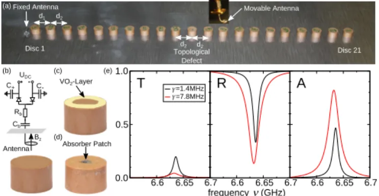
6L6 6L65 6L7 hLh hL5 CLh γ =CLBMHz =7L8MHz γ 6L6 6L65 6L7 6L6 6L65 6L7 frequency 2GHzv T R A ν FixedtAntenna Topological Defect DisctC Disct+C dC d+ d+ d+ MovabletAntenna 2av 2bv 2cv 2dv 2ev VO+-Layer AbsorbertPatch C-CV Cb UDC Rb Bz Antenna
FIG. 1. (a) The experimental set-up: The resonators are
sep-arated by distances d1 or d2 with d1 < d2. A central defect
is introduced by repeating the spacing d2; Various propos-als for the implementation of non-linear losses in the defect resonator: (b) A circuit with various module (sensing an-tenna, diode, threshold DC voltage); (c) An epitaxial growth of a material that experiences a thermally induced insulator-to-metal phase transition; (d) Our measurements involve a defect resonator, which includes a manually modulated ab-sorbing patch; (e) Measured transmittance T , reflectance R and absorption A for two different patches. The linewidth γ (1.4 and 7.8 MHz) of the reflected signal mainly characterizes the losses due to the absorbing patches.
high efficiency photonic limiters. In most occasions, how-ever, limiting action is achieved by a non-linear frequency shift of the transparency window of the photonic struc-ture. Such a shift is inherently small and, therefore, can-not provide broadband protection from high-power input. Other schemes, specifically in the microwave domain, ex-ploit PIN diodes (having spike leakage problems) [23], TR tubes or self-attenuating superconducting transmis-sion lines that require high power consumption [24]. To address these issues we have recently proposed the con-cept of reflective photonic limiters [25,26]. Such limiters reflect the high radiation, thereby, protecting themself -not just the receiving device– while they provide a strong resonant transmission for low incident radiation.
2 Here we propose the use of chiral coupled resonator
waveguides (C-CROW) with alternating short and long distances from one another (see Fig. 1), as a fertile plat-form to implement structurally robust reflective waveg-uide limiters with a wide DR. In the presence of a phase slip defect [27,28], chiral symmetry provides topological protection to a midgap defect localized mode [11,12]. For low incident power (or energy) it can provide high trans-mittance shielded from (positional) fabrication imperfec-tions. When (non-linear) losses at the defect resonator (triggered from high power - or energy- incident radia-tion) exceed a critical value, the resonant defect mode and the associated resonant transmission are dramati-cally suppressed turning the C-CROW highly reflective (not absorptive!) for a broad frequency range. As a result, the LDT increases with a consequent increase of the DR of the limiter. Using a microwave C-CROW arrangement we have tested experimentally the operational principle of this new class of TP reflective photonic limiter by in-vestigating the sensitivity and transport characteristics of the TP resonant defect mode in the presence of losses. The set-up (see Fig.1a) consists of N = 21 high index cylindrical resonators (radius r = 4mm, height h = 5mm, made of ceramics with refraction index n ≈ 6) with eigenfrequency around ν0 = 6.655 GHz and linewidth
γ = 1.4 MHz [29]. The resonators are placed at alternat-ing distances d1= 12 mm and d2= 14 mm corresponding
to strong (t1= 38 MHz) and weak (t2= 21 MHz)
evanes-cent couplings, respectively. A topological defect at the 11th resonator is introduced by repeating the spacing d2
[11, 12]. On the left hand side of the array, close to the first resonator, we have placed a kink antenna that emits a signal exciting the first TE1resonant mode of the
resonators. The structure is shielded from above with a metallic plate (not shown) where a movable loop antenna (receiving antenna) is mounted and is coupled to the 13th resonator. The kink antenna couples to the electric field that is in the xy-plane, whereas the loop antenna couples to the magnetic field, which is in the z-direction.
We assume that the defect resonator incorporates a nonlinear absorption mechanism, i.e. we assume that its losses are self-regulated depending on the strength of the incident radiation. One option to incorporate nonlin-ear losses is via an external element (fast diodes), see Fig.1(b). This option provides on-the-fly reconfigurabil-ity of the LT via an externally tuned DC voltage UDC.
An alternative mechanism is associated with temperature driven insulator-to-metal phase transition materials, like V O2[30–33], which can be deposited on top of the defect
resonator (see Fig. 1c).
In our experiment we are not concerned with the phys-ical origin of the nonlinear losses at the defect resonator. Rather we focus on demonstrating their effects on the transport properties of the photonic structure and thus establishing the operational principle of (structurally) robust reflective photonic limiters with wide
dynami-cal range. Therefore, we have included losses γD by
placing an absorbing patch on top of the resonator [see Fig. 1(d)]. This process results in a slight shift of the real part of the permittivity of the defect resonator, which we corrected by using resonators with slightly higher eigen-frequency. The linewidth γ has been used in order to quantify the losses of the resonators.
In Fig. 1(e) we show the transmittance T , reflectance R, and absorption A = 1 − T − R for two resonators with different losses. The transmittance is measured from the kink antenna to the loop antenna, which was positioned above the resonator. The reflectance is measured from the kink antenna. We observe that the transmittance of the stand-alone lossy resonator reduces as the losses increase, thus acting as a limiter. However this reduction comes to the expense of increasing absorption, i.e. the stand-alone lossy resonator acts as a sacrificial limiter.
The photonic structure is described by a one-dimensional (1D) tight-binding Hamiltonian
HP = X n νn|nihn| + X n tn(|nihn + 1| + |n + 1ihn|, (1)
where n = 1, 2, . . . , 21 enumerates the resonators, νn =
ν = ν0− iγ is the resonance frequency of the nth
indi-vidual resonator and tn(= t1 or t2) is the coupling
be-tween nearest resonators. The band-structure consists of two mini-bands ν0− t1− t2 < ν < ν0− |t1− t2| and
ν0+ |t1− t2| < ν < ν0+ t1+ t2 separated by a finite
gap of width 2|t1− t2|. In the presence of the defect
res-onator at n0= 11 a TP defect mode at νD= ν0[11],[12]
is created. This mode is exponentially localized around the defect resonator. Its shape, in the limit of infinite many resonators, is [11] ψnD∼ ( 1 √ ξe −|n−n0|/ξ; n odd 0; n even (2) where ψDn is the amplitude of the defect mode at the nth
resonator and ξ = 1/ ln(t1/t2) is the so-called localization
length of the mode [11]. Hamiltonian Eq. (1) is invariant under a chiral symmetry i.e. {HP, C} = 0 where {· · ·}
indicates an anti-commutation and C = Peven − Podd
satisfies the relations C2= 1 (P
even/odd is the projection
operator in the even/odd sites). The staggering form of ψD is a consequence of the chiral symmetry which
also provides topological protection to ψDand ν
Dagainst
reasonable variations of t1and t2 [11,12].
We are modeling the transmitted (reflected) antenna, coupled to nT = 1 (nR = 13) resonator, by a 1D
semi-infinite tight-binding lattice with coupling constant tL =
(t1+ t2)/2 and on-site energies νL= ν0. The associated
scattering matrix takes the form [35] ˆ S = −ˆ1+2i sin k tL WT 1 Hef f − ν W ; Hef f = HP+ eik tL W WT, (3)
FIG. 2. Measurements of the (a) transmittance T ; (b)
re-flectance R; and (c) absorption A for the C-CROW of Fig.1.
We considered two different values of γD = 1.4 MHz and
γD = 7.8 MHz. All other resonators have γ = 1.4 MHz.
Numerical calculations for the (d) transmittance T ; (e) re-flectance R and (f) absorption A where we assumed that all resonators are lossless, i.e. γ = 0, apart from the defect
res-onator which has γD = 1.4 MHz (solid lines) and γD = 7.8
MHz (dashed lines).
where ˆ1 is the 2 × 2 identity matrix, Wnm =
wTδn,nTδm,1+ wRδn,nRδm,2 is a N × 2 matrix that
de-scribes the coupling between the array and the antennas, ν = νL+ 2tLcos k is the frequency of propagating waves
at the antennas and k is their associated wavevector. When the system is coupled to the antennas, ψD
becomes a quasi-localized resonant mode at frequency νD≈ ν0, with a large but finite lifetime τ :
τ−1∼ ψD eik tL W WT ψD = |wT|2|ψD1| 2+|w R|2|ψD13| 2, (4) where |ψD
1|2, |ψD13|2are given by Eq. (2).
The measured transmittance T = |S12|2, reflectance
R = |S11|2and absorption A = 1 − T − R versus
frequen-cies ν of the C-CROW (with global γ = 1.4 MHz = γD)
are shown in Figs. 2(a,b,c) (solid lines). Measurements of the widths of the mini-bands and of the gap allow us to extract the couplings t1 = 38 MHz, t2= 21 MHz. We
find that the presence of the defect resonator results in a transmission peak at ν = νD inside the band gap. A
fitting of the height of this peak, for various γD values,
gives wT = 10.915 MHz, wR= 3.6875 MHz (see Fig. 3).
The small peak in the absorption (solid line in Fig.2(c)) is associated with the fact that all our resonators have a small ohmic component. In Fig. 2(a) we also report (dashed lines) the measured transmittance for a defect with additional losses, i.e. γD = 7.8 MHz. We find that
even a small increase in γDstrongly suppresses the
reso-nant transmission, see Fig.2(a).
In Fig.2(b) we show R(ν) of the C-CROW for γD =
FIG. 3. The transmittance T (up) and absorption A
(down) versus γD: (Left) for the C-CROW with resonator losses γ = 1.4MHz (black lines-numerics/circles-experiment) and for the stand-alone resonator (blue dashed-dotted
lines-numerics/diamonds-experiment). (Right) Numerics for the
ideal C-CROW (red dashed lines) with γ = 0 at all other resonators. Symbols (blue dashed-dotted lines) correspond to measurements (numerics) of T and A for the stand-alone resonator. Shadowed areas indicate deviations in T, A due to randomness in the couplings.
1.4 MHz and γD = 7.8 MHz (solid and dashed lines,
re-spectively). We find that the suppression in T (νD) is
ac-companied by an increase in R(νD). Moreover A(νD) is
decreasing as γDincreases, see Fig.2(c). In other words,
our photonic structure becomes reflective (not absorp-tive) as the losses of the defect resonator increase. This behavior is in distinct contrast to the case of a single (sacrificial) lossy resonator [see Fig.1(e)] where the drop in transmittance is associated with an increase of absorp-tion. These features are also observed in the simulations of an ideal C-CROW where all resonators have zero in-trinsic losses γ = 0, see Figs.2(d,e,f).
An overview of the measured (black circles) T (νD),
A(νD) and the corresponding numerical results (black
solid lines) for the C-CROW of Fig.1 versus γD are
re-ported at the left column of Fig. 3. We find that an increase of γD leads to a decrease of T (νD) and A(νD)
of the photonic structure. This behavior is contrasted with the measurements (diamonds) and numerical calcu-lations (dashed-dotted lines) of a stand-alone lossy res-onator. In the latter case we observe relatively large T values T ∼ 10−1as opposed to T ∼ 10−4for the photonic structure, i.e. ultralow LT. For moderate γD-values the
absorption of the stand-alone resonator reaches large val-ues A(γD= 0.004 GHz) ≈ 0.8 corresponding to low LDT.
In contrast, the C-CROW takes absorption values, which are at least one order of magnitude smaller (high LDT). At the right column of Fig.3, we report the simulations
4
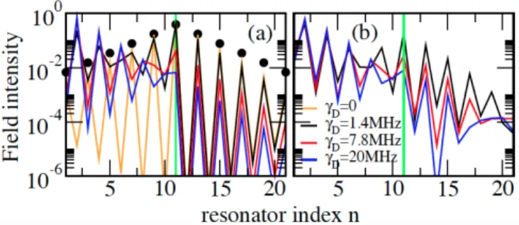
FIG. 4. (a) Simulations for an ideal C-CROW consisting of
lossless resonators with γ = 0. Filled black circles correspond
to Eq.2for the defect mode profile. Solid lines correspond to
the simulations of the resonant defect mode profile for various
γD. For symmetry reasons we assumed that the antennas
are coupled to the first and last resonator. (b) Experimental resonant mode profiles for various γD-values. The measured losses at all resonators are γ = 1.4 MHz.
for T (νD), A(νD) for an ideal (γ = 0) C-CROW (dashed
lines) versus the losses γDof the defect resonator. Again,
we compare these results to the theoretical/experimental (dash-dotted lines/diamonds) results for the stand-alone lossy resonator. Both cases show the same qualitative be-havior. However, the C-CROW shows a two-order lower LT (i.e. smaller γD-value for which the decay of
transmit-tance occurs) as compared to a stand-alone resonator. At the same time the LDT of the photonic structure is at least two orders of magnitude higher than the one associ-ated with the stand-alone resonator. The latter acquires a maximum value of absorption A ≈ 0.8 at γD ≈ 0.01
as opposed to A ≈ 0.01 acquired by the C-CROW. The maximum absorption for the photonic structure occurs at much lower values of γD∼ 10−4which in the case of a
non-linear lossy mechanism correspond to rather small, and therefore harmless, incident radiation.
The transport features of the TP resonant mode have been further investigated in case of positional random-ness corresponding to a box distribution for the coupling constants ˜t1,2∈ [t1,2− 2M Hz, t1,2+ 2M Hz]. The
shad-owed area in Fig. 3indicates the variations in T, A. For γD ≈ 0 (not shown) the resonant frequency ν0 ≈ 6.655
GHz remains protected and the resonant transmission is unaffected for both a perfect C-CROW γ = 0 and for resonator with losses γ = 1.4MHz. Moreover the exper-imental data in Fig. 3 incorporate an intrinsic disorder associated with the variation of the bare resonance fre-quencies, within a range of 1MHz, and the precision of the resonator positioning, of the order of 0.2mm (cou-pling uncertainty ≈ 500 kHz). Nevertheless, the trans-port features remain largely unaffected, see Fig. 3.
The fragility of the resonant localised mode at moder-ate γD-values is further analysed in Fig. 4. In Fig. 4(a)
we report the simulated resonant defect fields for an ideal C-CROW (i.e. γ = 0) and for various γD-values.
For γD = 0, a nice agreement between the numerics
and Eq. (2) is observed, indicating that the coupling to the antennas does not affect the resonant mode profile. As γD increases, a gradual deviation from the profile of
Eq. (2) occurs and eventually a suppression of the defect mode is observed. At γD = 20 MHz the resonant
local-ized mode is suppressed enough so that the field intensity in the vicinity of the defect lossy resonator is two orders smaller than the corresponding one for γD = 0. Thus
the lossy defect resonator is protected from damages in-duced by heat or electrical breakdown. For the C-CROW of Fig.1a it implies a huge increase in its DR. The com-parison with the experimental data [see Fig.4(b)], where γ = 1.4MHz, indicates that the underlying mechanism which is responsible for the destruction of the resonant defect mode remains unaffected.
The destruction of the resonant defect mode can be un-derstood intuitively as a result of a competition between two mechanisms that control the dwell time of photons in the resonant state. The first one is associated with the boundary losses due to the coupling of the photonic struc-ture to the antennas. It results to a resonant linewidth Γedge ∼ τ−1, see Eq. 4. The other mechanism is
as-sociated with bulk losses and it leads to an additional broadening of the resonance linewidth. From first order perturbation theory Γbulk≈ γD|ψ11|2+ γPn6=11|ψn|2=
(γD − γ)/ξ + γ. For small values of γD such that
Γbulk < Γedge, the dwell time is determined by Γedge
and it is essentially constant. Thus the absorption of the photons that populate the resonant state increases, as they are trapped for relatively long time in the lossy C-CROW [see the peak of the black line in Fig. 2(c)]. When Γbulk ≈ Γedge, the dwell time itself begins to
di-minish, and the resonant mode is spoiled. For even larger values of γD the photons do not dwell at all in the
res-onant state and reflection from the whole structure be-comes the dominant mechanism. As a result, the absorp-tion decreases to zero. The above argumentaabsorp-tion applies equally well for the stand-alone defect and for the pho-tonic structure. However, in the latter case the condition for the destruction of the resonant mode Γbulk ≈ Γedge
is achieved for exponentially smaller values of γD. It is
exactly this effect that our proposal is harvesting in order to increase the damaging threshold (and the DR) of the photonic waveguide limiter.
We acknowledge partial support from AFOSR via MURI grant FA9550-14-1-0037 (T.K.) and LRIR14RY14COR (I.V.). (E. M.) acknowledges partial support from Wesleyan University and from NSF EFMA-1641109. The stay of (T.K.) at LPMC-CNRS was supported by CNRS.
[1] L. Lu, J. D. Joannopoulos and M. Soljaˇci´c, Nat. Phot. 8,
[2] S. Raghu and F. D. M. Haldane, Phys. Rev. A 78, 033834 (2008).
[3] Z. Wang, Y. Chong, J. D. Joannopoulos, and M. Soljacic, Nature (London) 461, 772 (2009).
[4] M. Hafezi, E. A. Demler, M. D. Lukin, and J. M. Taylor, Nat. Phys. 7, 907 (2011).
[5] K. Fang, Z. Yu, and S. Fan, Nat. Photonics 6, 782 (2012). [6] T. Kitagawa, M. A. Broome, A. Fedrizzi, M. S. Rudner, E. Berg, I. Kassal, A. Aspuru-Guzik, E. Demler, and A. G. White, Nat. Commun. 3, 882 (2012).
[7] A. B. Khanikaev, S. H. Mousavi, W.-K. Tse, M. Kar-garin, A. H. MacDonald, and G. Shvets, Nat. Mater. 12, 233 (2013).
[8] M. Hafezi, S. Mittal, J. Fan, A. Migdall, and J. M. Taylor, Nat. Photonics 7, 1001 (2013).
[9] M. C. Rechtsman, J. M. Zeuner, Y. Plotnik, Y. Lumer, D. Podolsky, F. Dreisow, S. Nolte, M. Segev, and A. Sza-meit, Nature (London) 496, 196 (2013).
[10] S. Malzard, C. Poli and H. Schomerus, Phys. Rev. Lett. 115, 200402 (2015).
[11] J. K. Asb´oth and L. Oroszl´any, A. P´alyi, A Short Course
on Topological Insulators, Lecture Notes in Physics 919, Cambridge University Press (2016)
[12] C. Poli, M. Bellec, U. Kuhl, F. Mortessagne, H. Schome-rus, Nat. Comm. 6, 6710 (2015)
[13] L. W. Tutt and T. F. Boggess, Prog. Quant. Electr. 17, 299-338 (1993)
[14] A. E. Siegman, Appl. Opt. 1, 739-744 (1962).
[15] J. E. Geusic, S. Singh and D. W. Tipping and T. C. Rich, Phys. Rev. Lett. 19, 1126-1128 (1967).
[16] M. Scalora, J. P. Dowling, C. M. Bowden and M. J. Bloe-mer, Phys. Rev. Lett. 73, 1368-1371 (1994)
[17] T. F. Boggess, S. C. Moss, I. W. Boyd and A. L. Smirl, Opt. Lett. 9, 291-293 (1984).
[18] M. Heinrich, F. Eilenberger, R. Keil, F. Dreisow, E.
Suran, F. Louradour, A. T¨unnermann, T. Pertsch, S.
Nolte and A. Szameit, Opt. Ex. 20, 27299-27310 (2012). [19] M. Scalora, J. P. Dowling, C. M. Bowden and M. J.
Bloe-mer, Phys. Rev. Lett. 73, 1368 (1994).
[20] M. Larciprete, C. Sibilia, S. Paoloni, M. Bertolotti, F. Sarto and M. Scalora, J. Appl. Phys. 93, 5013 (2003). [21] X. Liu, J. W. Haus, M. S. Shahriar, Opt. Exp. 17,
2696-2706 (2009); B. Y. Soon, J. W. Haus, M. Scalora and C. Sibilia, Opt. Exp. 11, 2007-2018 (2003).
[22] L. W. Cross, M. J. Almalkawi, V. K. Devabhaktuni, IEEE Transactions on Electromagnetic Compatibility 55, 1100 (2013)
[23] R.V.Garver, Microwave Diode Control Devices, Artech House,Inc. (1976).
[24] J. C. Booth, D. A. Rudman, R. H. Ono, IEEE Transac-tions on Applied Superconductivity 13, 305 (2003). [25] E. Makri and H. Ramezani and T. Kottos and I.
Viteb-skiy, Phys. Rev. A 89, 031802(R) (2014).
[26] E. Makri, T. Kottos and I. Vitebskiy, Phys. Rev. A 91, 043838 (2015).
[27] V.M. Apalkov, M. E. Raikh, Phys. Rev. Lett. 90, 253901 (2003); E. A. Avrutin and M. E. Raikh, Sov. Phys. Tech. Phys. 33, 1170 (1988).
[28] J. S. Foresi, P. R. Villeneuve, J. Ferrera, E. R. Thoen, G. Steinmeyer, S. Fan, J. D. Joannopoulos, L. C. Kimerling, H. I. Smith and E. P. Ippen, Nature 390, 143 (1997). [29] M. Bellec, U. Kuhl, G. Montambaux and F. Mortessagne,
Phys. Rev. B 88, 115437 (2013).
[30] J. H. Bechtel and W. L. Smith, Phys. Rev. B 13, 3515-3522 (1976).
[31] A. Crunteanu, J. Givernaud, P. Blondy, J.-C. Orlianges, C. Champeaux, A. Catherinot, Advanced Microwave and Millimeter Wave Technologies Semiconductor De-vices Circuits and Systems, edited M. Mukherjee, InTech, 35-56 chap. 3 (2004).
[32] P. Phoempoon and L. Sikong, The Scientific World Jour-nal 2014, Article ID 841418 (2014)
[33] A. L. Pergament, G. B. Stefanovich, N. A. Kuldin and A. A. Velichko, ICMP 2013, Article ID 960627 (2013) [34] P. Markos and C. M. Soukoulis, Wave Propagation: From
Electrons to Photonic Crystals and Left-Handed Materi-als, Princeton University Press, (Princeton, U.S.) (2008) [35] S. Datta, Electronic Transport in Mesoscopic Systems,