HAL Id: hal-02539636
https://hal.archives-ouvertes.fr/hal-02539636
Submitted on 10 Apr 2020
HAL is a multi-disciplinary open access
archive for the deposit and dissemination of
sci-entific research documents, whether they are
pub-lished or not. The documents may come from
teaching and research institutions in France or
abroad, or from public or private research centers.
L’archive ouverte pluridisciplinaire HAL, est
destinée au dépôt et à la diffusion de documents
scientifiques de niveau recherche, publiés ou non,
émanant des établissements d’enseignement et de
recherche français ou étrangers, des laboratoires
publics ou privés.
Silicon chip-integrated fiber couplers with sub-decibel
loss
Daniel Benedikovic, Carlos Alonso-Ramos, Sylvain Guerber, Cecilia Dupre,
Bertrand Szelag, Xavier Le Roux, Pavel Cheben, Daivid Fowler, Guillaume
Marcaud, Vladyslav Vakarin, et al.
To cite this version:
Daniel Benedikovic, Carlos Alonso-Ramos, Sylvain Guerber, Cecilia Dupre, Bertrand Szelag, et
al..
Silicon chip-integrated fiber couplers with sub-decibel loss.
SPIE OPTO Smart Photonic
and Optoelectronic Integrated Circuits XXII, Jan 2020, San Francisco, California, United States.
�10.1117/12.2543489�. �hal-02539636�
Silicon chip-integrated fiber couplers with sub-decibel loss
Daniel Benedikovic
a, *, Carlos A. Alonso-Ramos
a, Sylvain Guerber
b, Cecilia Dupre
b, Bertrand
Szelag
b, Xavier Le Roux
a, Pavel Cheben
c, Daivid Fowler
b, Guillaume Marcaud
a, Vladyslav
Vakarin
a, Diego Perez-Galacho
d, Delphine Marris-Morini
a, Eric, Cassan
a, Charles Baudot
e, Frederic
Boeuf
e, and Laurent Vivien
aa
Université Paris-Saclay, CNRS, Centre de Nanosciences et de Nanotechnologies, 91120, Palaiseau,
France
b
LETI University Grenoble Alpes and CEA, LETI, Minatec Campus, F-38054 Grenoble, France;
c
National Research Council Canada, Ottawa, ON K1A 0R6, Canada
d
Spain ITEAM Research Institute, Universitat Politècnica de València, Camino de Vera s/n, 46022,
Valencia, Spain
e
STM Technology R&D, STMicroelectronics SAS, 850 Rue Jean Monnet, 38920 Crolles, France
ABSTRACT
Silicon nanophotonics represents a scalable route to deploy complex optical integrated circuits for multifold applications, markets, and end-users. Most recently, applications such as optical communications and interconnects, sensing, as well as quantum-based technologies, among others, present additional opportunities for integrated silicon nanophotonics to expand its frontiers from laboratories to industrial product development. Within a wide set of functionalities that silicon nanophotonic chips can afford, the availability of low-loss optical input/output interfaces has been regarded as a major practical obstacle that hampers long-term success of integrated photonic platforms. Indeed, fiber-chip interfaces based on diffraction gratings are an attractive solution to resonantly couple the light between planar waveguide circuits and standard single-mode optical fibers. Surface grating couplers provide much more alignment tolerance in fiber attach compared with most conventional edge-coupled alternatives, while retaining the much-needed control of the fiber placement on the chip surface and wafer-level-test capability that the in-plane convertors lack. Here, we report on our recent advances in the development of high-performance fiber-chip grating couplers that exploit the blazing effect. This is achieved with well-established dual-etch processing in interleaved teeth-trench arrangements or using L-shaped grating-teeth-profile geometries. The first demonstration of the L-shaped-based grating coupler yielded a coupling loss of -2.7 dB, seamlessly fabricated into a 300-mm foundry manufacturing process using 193-nm deep-ultraviolet stepper lithography. Moreover, silicon metamaterial L-shaped fiber couplers may promote robust sub-decibel coupling of light, reaching a simulated coupling loss of -0.25 dB, while featuring device layouts (>120 nm) compatible with lithographic technologies in silicon semiconductor foundries.
Keywords: silicon photonics, complementary metal-oxide semiconductor technology, fiber-chip optical interface, surface grating couplers, sub-wavelength grating metamaterials, deep-ultraviolet lithography, immersion lithography
*
e-mail: [email protected]
1. INTRODUCTION
Silicon (Si) nanophotonics has been recognized as a viable integration technology to realize compact optical chips. For Si nanophotonics, silicon-on-insulator (SOI) substrates have been established as prominent and widely accessible material platforms for many applications, markets, and end-users1-3. Although pure SOI platforms, with Si as a waveguide core, definitely lacks active on-chip functionalities4-8, the fundamental passive function of light guiding is their key advantage9,10. Moreover, dense integration ability, low-cost fabrication, high-yield production within Si-foundry-compatible environment are other advantages offered by SOIs.
However, device miniaturization to sub-micron scales complicates coupling of light to or from high-index-contrast SOI chips. Direct butt-coupling is largely inefficient, with losses in excess of -30 dB. The coupling is particularly difficult
due to the mismatch in mode sizes between Si waveguides and standard single-mode optical fibers11-14. This is a serious obstacle for many nanophotonic applications in areas such as communications, interconnects, or quantum information sciences, amongst other. The quest for low-loss light coupling in and out of the chip drives the development in SOI nanophotonics for many years and definitely remains a very active research area12-14. In this buoyant field, edge-coupled15-20 and grating-coupled21-56 optical interfaces are leading solutions.
With edge couplers, low loss, low polarization dependence, and wideband operation are typically obtained. However, limited positioning on chip edges, the call for high-quality facet preparation, and tight alignment tolerances are drawbacks that make them less-suited for wafer-scale testing. In opposite, surface grating couplers have a much better alignment margins to fiber attach and enable straightforward on-wafer tests. The latter feature not only facilitates integration21 and packaging22, but also bring considerable value in terms of early-stage error detection, mass-volume deployment, or process automation23,24.
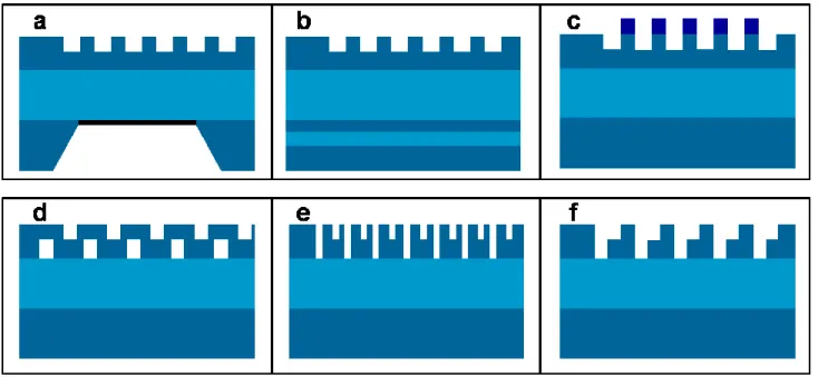
A large number of different grating couplers has been proposed and demonstrated over the course of recent years. The state-of-the-art surface grating couplers, both in designs and experiments, may give coupling loss well below 1-dB across the near-infrared (near-IR) wavelengths. These achievements are close to the best reported values for edge couplers. Of course, due to the dispersive operation principle of grating coupler, those levels of coupling loss are associated with lower bandwidths, typically of about 30-nm to 40-nm for a 1-dB drop. Leading approaches for sub-decibel (sub-dB) grating coupler designs are schematically summarized in Fig. 1.
Figure 1. State-of-the-art approaches to couple light between SOI chip and single-mode optical fiber with a sub-decibel loss using surface grating couplers: backside-processed SOIs with (a) metal mirror28-34 and (b) Bragg reflector21,23,35,36, (c) over-layered waveguides37-40, (d) multi-level arrangements42-46, (e) interleaved geometry48-50, and (f) L-shaped profile51-56.
Improved coupling loss between SOI chips and optical fibers can be obtained by forming bottom metal mirrors28-34 or Bragg reflectors21,23,35,36, both embedded at the chip backside, as shown in Figs. 1(a) and 1(b), respectively. However, local claddings adjustment, backside substrate processing, or flip-chip bonding are steps that bring more complexity in fabrication, and thus increase the production cost. As an alternative, the coupling loss can be enhanced by engineering the vertical device symmetry37-56. The broken device symmetry yields improved coupling in a desired direction. In a simplest case, this can be achieved through structures with custom-designed SOIs or etching depths25-27. More advanced solutions include low- and high-index overlays37-40 or multi-layer41 and multi-level42-46 grating architectures, as shown in Figs. 1(c) and 1(d), respectively. In recent years, we elaborated on low-loss grating couplers in SOI waveguides that exploit an unique blazing effect. In blazed coupler designs, the radiation performance is controlled with two asymmetric scatterers realized thanks to two different etch levels, typically used in waveguide and/or device fabrication48,49. Such grating arrangement allows for a full control over the interference pattern within the device. Fiber-chip grating couplers based on interleaved48-50 (Fig. 1(e)) and L-shaped51-56 (Fig. 1(f)) waveguides have been demonstrated, showing a rather
good potential for low-loss Si chip interfacing. Moreover, this design concept can also be optimized for a vertical coupling in two polarization states53 or even exploited in different waveguide platforms55,56.
In this work, we present our recent advances in development of low-loss fiber-chip grating couplers implemented on SOI waveguides. In specific, high-performance fiber-chip grating couplers exploit the unique blazing effect. This is achieved via established double-etch processing using L-shaped grating-teeth-profile geometry. The uniform L-shaped coupler yielded a coupling loss of -2.7 dB, seamlessly fabricated into a 300 mm Si-foundry process with 193-nm deep-ultraviolet stepper lithography51. Moreover, Si metamaterial-engineered L-shaped fiber couplers may promote robust coupling of light between SMF-28 fibers and SOI waveguides. Simulation suggest a fiber-chip coupling loss down to -0.25 dB, while device layouts remain compatible with established patterning technologies in Si nanophotonic foundries54.
The manuscript is organized as follows. After the introductory Section 1, uniform designs and experimental results on L-shaped waveguide grating coupler are described in Section 2. In Section 3, L-L-shaped coupler designs engineered with sub-wavelength gratings are presented. Finally, conclusions are drawn in Section 4.
2. UNIFORM L-SHAPED GRATING COUPLERS
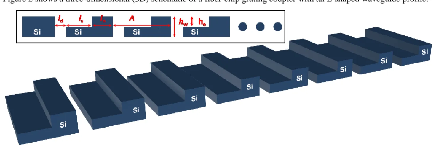
Figure 2 shows a three-dimensional (3D) schematic of a fiber-chip grating coupler with an L-shaped waveguide profile.
Figure 2. 3D Schematic of an uniform off-chip fiber coupler with an L-shaped grating-teeth-profile. Inset: Side view of the surface grating coupler with vertical (hw and he) and longitudinal (ld, ls, ln, and Λ) device parameters.
The coupler is designed for a SOI platform with 310-nm Si (hw) and 720-nm buried oxide (BOX). The grating coupler
features on L-shaped geometry with deep (hw =300 nm) and partial (he = 150 nm) etches that form a diffraction grating
with the pitch (Λ), full- and shallow-etch trenches of lengths ld and ls, respectively, and unetched Si segments of length
ln). Grating coupler maximizes transmission for transverse electric (TE) polarization at a wavelength of 1.55 μm.
Figure 3. 2D mapping of the grating directionality versus lengths of the shallow-etch trenches and unetched teeth for various lengths of deep-etch trenches: (a) ld = 50 nm; (b) ld = 100 nm; (c) ld = 150 nm; and (d) ld = 200 nm.
Figure 3 shows a collection of 2D maps of a grating coupler directionality as functions of all three longitudinal dimensions (lengths of deep- and shallow-etch trenches (ld and ls) as well as the unetched grating coupler segments (ln)).
and an optical power radiated into the bottom Si handle. Simulations reveal that exceptional levels of grating directionality can be achieved, typically larger than 90% for a wide range of device dimensions. However, due to the large index discontinuity between the Si access waveguide and deep-etch grating trench, large back-reflection in 15% - 30% range typically appear at this junction. An uniform coupler has following parameters51: ld = 120 nm, ls = 290 nm, ln
=310 nm, Λ = 710 nm, and 30 diffraction periods.
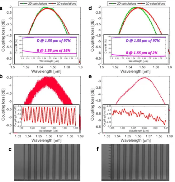
Figure 4. Results (design, experiments, and SEM images) on L-shaped fiber-chip grating couplers without (from (a) to (c)) and with (from (d) to (f)) a short SWG reflection-canceling region.
Figure 4 shows design and experimental results for uniform L-shaped grating couplers without (in Figs. 4(a) to 4(c)) and with (in Figs. 4(d) to 4(f)) a short reflection-canceling region51. This region was implemented at the beginning of the coupler thanks to the SWG metamaterials, i.e. interleaved etched and unetched Si segments with a periodicity much lower that the 1st Bragg reflection zone9,10. The reflection-canceling region was positioned in a transversal grating direction (see scanning electron microscopy (SEM) image of device in Fig. 4(f)). In theory, both grating coupler designs provided a high directionality up to 97% at 1.55 µm. Moreover, substantial decrease in grating back-reflections was obtained for design with a short SWG region. Back-reflections were reduced from 16% down to 2% at 1.55 µm for grating couplers without and with a SWG region. Spectral evolution of the grating directionality (D) and reflectivity (R) is shown in insets of Figs 4(a) and 4(d), respectively. Both coupler designs yielded a coupling loss of -2.1 dB.
L-shaped grating couplers were fabricated on 300 mm SOI platform using Si-foundry process in STMicroelectronics.
losses of -3.4 dB and -2.7 dB were measured, with a -3dB bandwidths of 46 nm and 62 nm, respectively, for respective
L-shaped grating couplers. Furthermore, from Fabry-Perot ripples, we estimated back-reflections of about 8% and 1%
for designs without and with a short SWG region51.
3. APODIZED L-SHAPED GRATING COUPLERS
Figure 5 shows a 3D schematic and a part of mask layout for an apodized L-shaped surface grating coupler engineered with SWG metamaterials. The apodized coupler region comprises full- and shallow-etch trenches with a synthesized subwavelength grating (SWG) metamaterial, followed by a uniform coupler region. This concept jointly provides enough degrees of design freedom to control the grating directionality and out-radiated field profile of the grating mode simultaneously. Design details are reported elsewhere54. As shown earlier, the grating directionality is controlled via longitudinal parameters, while SWG metamaterials in the grating trenches allow for proper field matching between profiles of the diffracted beam and the near-Gaussian mode of the SMF-28 fiber.
Figure 5. 3D schematic of an apodized off-chip fiber coupler with an L-shaped grating-teeth-profile and SWG metamaterials. Inset: Top view on the mask layout of an L-shaped grating coupler with 3 apodized periods.
L-shaped grating couplers with engineered SWG metamaterials can yield a low-loss towards a SMF-28 optical fibers.
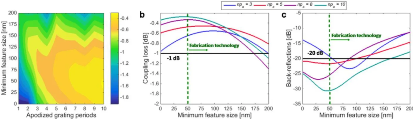
Figure 6(a) sums up the simulated coupling loss between an integrated Si waveguide coupler with apodized L-shaped profile and an optical fiber. The 2D map of fiber-chip coupling loss, was calculated at a wavelength of 1.55 µm as functions of the number of apodized grating periods (npa = 1 to 10) and the minimum width of the etched SWG holes up
to 200 nm. It can be observed that a wide set of grating coupler designs can be chosen to afford robust coupling with losses below 1 dB.
Figure 6. (a) 2D map of simulated coupling loss of apodized L-shaped grating couplers versus the number of apodized periods and minimum feature size of the SWG holes. Simulated performance of apodized L-shaped grating couplers as a function of a minimum feature size of lateral SWG holes for different number of apodized periods: (b) coupling loss and (c) back-reflections.
Detailed look on the estimated performance (coupling loss and back-reflections) of L-shaped grating couplers is shown in Figs. 6(b) and 6(c), respectively. Figure 6(b) shows a coupling loss versus critical dimensions of SWG holes and this for different apodized grating coupler designs. Indeed, sub-dB coupling losses were calculated for considered grating coupler designs over a wide range of minimum feature sizes. The L-shaped grating coupler designs are well-suited to keep low levels of fiber-chip coupling loss for a significantly relaxed criteria on minimum feature sizes. In other words, the proposed grating coupler designs are compatible with established lithographic technologies typically used in Si-foundries, including emerging high-end immersion lithography (critical dimensions of ~50 nm) as well as more conventional deep-ultraviolet optical lithography (critical dimensions typically larger than 100 nm). The grating coupler reflectivity versus critical dimensions of SWG holes is shown in Fig. 6(c). The calculated back-reflections of apodized
L-shaped grating couplers is found to be typically below -20 dB for available range of critical dimensions.
4. CONCLUSIONS
In this work, we reported on recent results in development of low-loss fiber-chip grating couplers implemented on SOI waveguides. Low-loss fiber-chip grating couplers exploited the unique blazing effect thanks to established double-etch processing with a robust L-shaped waveguide geometry. The uniform grating coupler was seamlessly fabricated into a 300 mm Si-foundry process with 193-nm deep-ultraviolet lithography, yielding a peak coupling loss of -2.7 dB and back-reflections of about -20 dB. Moreover, Si metamaterial-engineered L-shaped fiber couplers were developed to promote robust coupling of light between SMF-28 fibers and SOI waveguides. Simulation suggested a fiber-chip coupling loss down to -0.25 dB, while device layouts are still compatible with available lithographic technologies presently used in Si nanophotonic foundries. This work holds promises to further develop robust, reliable, and low-cost optical interfaces in integrated Si nanophotonics.
ACKNOWLEDGEMENTS
This work has received funding from the European Research Council (ERC) under the European Union’s Horizon 2020 Research and Innovation Program (ERC POPSTAR – grant agreement No 647342). This work was also partially founded by Agence Nationale de la Recherche (ANR) MIRSPEC, Nano 2020 under Important Projects of Common European Interest (IPCEI).
REFERENCES
[1] L. Vivien and L. Pavesi, Handbook of Silicon Photonics (CRC Press, 2013).
[2] J. Chilles and S. Fathpour, “Silicon photonics beyond silicon-on-insulator,” Journal of Optics 19, 053001 (2017). [3] A. Rahim, T. Spuesens, R. Baets, and W. Bogaerts, “Open-Access Silicon Photonics: Current Status and Emerging
Initiatives,” Proceedings of the IEEE 106, 2313–2330 (2018).
[4] S. Wirths, R. Geiger, N. von den Driesch, G. Mussler, T. Stoica, S. Mantl, Z. Ikonic, M. Luysberg, S. Chiussi, J. M. Hartmann, H. Sigg, J. Faist, D. Buca, and D. Grutzmacher, “Lasing in direct-bandgap GeSn alloy grown on Si,“ Nature Photonics 9, 88-92, (2015).
[5] M. Berciano, G. Marcaud, P. Damas, X. Le Roux, P. Crozat, C. Alonso Ramos, D. Pérez Galacho, D. Benedikovic, D. Marris-Morini, E. Cassan, and L. Vivien, “Fast linear electro-optic effect in a centrosymmetric semiconductor ,” Communications Physics 1, Article number 64, 1-9 (2018).
[6] L. Virot, D. Benedikovic, B. Szelag, C. Alonso-Ramos, B. Karakus, J.-M. Hartmann, X. Le Roux, P. Crozat, E. Cassan, D. Marris-Morini, C. Baudot, F. Boeuf, J.-M. Fédéli, C. Kopp, and L. Vivien, “Integrated waveguide PIN photodiodes exploiting lateral Si/Ge/Si heterojunction,” Optics Express 25, 19487-19496, (2017).
[7] D. Benedikovic, L. Virot, G. Aubin, F. Amar, B. Szelag, B. Karakus, J.-M. Hartmann, C. Alonso-Ramos, X. Le Roux, P. Crozat, E. Cassan, D. Marris-Morini, C. Baudot, F. Boeuf, J.-M. Fédéli, C. Kopp, and L. Vivien, “25 Gbps low-voltage hetero-structured silicon-germanium waveguide pin photodetectors for monolithic on-chip nanophotonic architectures,” Photonics Research 7, 437-444, (2019).
[8] D. Benedikovic, L. Virot, G. Aubin, J.-M. Hartmann, F. Amar, B. Szelag, X. Le Roux, C. Alonso-Ramos, P. Crozat, E. Cassan, D. Marris-Morini, C. Baudot, F. Boeuf, J.-M. Fédéli, C. Kopp, and L. Vivien, “Comprehensive Study on Chip-Integrated Germanium Pin Photodetectors for Energy-Efficient Silicon Interconnects,” IEEE Journal of Quantum Electronics 56, Article Sequence Number 8400409, (2020).
[9] R. Halir, A. Ortega-Moñux, D. Benedikovic, G. Z. Mashanovich, J. G. Wangüemert-Pérez, J. H. Schmid, Í. Molina-Fernández, and P. Cheben, “Subwavelength-Grating Metamaterial Structures for Silicon Photonic Devices,” Proceedings of the IEEE 106, 2144-2157 (2018).
[10] P. Cheben, R. Halir, J. H. Schmid, H. A. Atwater, and D. R. Smith, “Subwavelength integrated photonics,” Nature 560, 565–572 (2018).
[11] D. Taillaert, W. Bogaerts, P. Bienstman, T. F. Krauss, P. Van Dale, I. Moerman, S. Verstuyft, D. De Messel, and R. Baets, “An out-of-plane grating coupler for efficient butt-coupling between compact planar waveguides and single-mode fibers,” IEEE Journal of Quantum Electronics 38, 949–955 (2002).
[12] G. Son, S. Han, J. Park, K. Kwon, and K. Yu, “High-efficiency broadband light coupling between optical fibers and photonic integrated circuits,” Nanophotonics 7, 1845–1864 (2018).
[13] D. Vermeulen and C. V. Poulton, “Optical Interfaces for Silicon Photonic Circuits,” Proceedings of IEEE 106, 2270–2280 (2018).
[14] R. Marchetti, C. Lacava, L. Carroll, K. Gradkowski, and P. Minzioni, “Coupling strategies for silicon photonics integrated chips,” Photonics Research 7, 201–239 (2019).
[15] P. Cheben, D.-X. Xu, S. Janz, and A. Densmore, “Subwavelength waveguide grating for mode conversion and light coupling in integrated optics,” Optics Express 14, 4695–4702 (2006).
[16] P. J. Bock, P. Cheben, J. H. Schmid, J. Lapointe, A. Delâge, S. Janz, G. C. Aers, D.-X. Xu, A. Densmore, and T. J. Hall, “Subwavelength grating periodic structures in silicon-on-insulator: a new type of microphotonic waveguide,” Optics Express 18, 20251–20262 (2010).
[17] T. Barwicz, A. Janta-Polczynski, M. Khater, Y. Thibodeau, R. Leidy, J. Maling, S. Martel, S. Engelmann, J. S. Orcutt, P. Fortier, and W. M. J. Green, “An O-band metamaterial converter interfacing standard optical fibers to silicon nanophotonics waveguides,” in Optical Fiber Communication Conference (OFC, 2015), paper Th3F.3. [18] P. Cheben, J. H. Schmid, S. Wang, D.-X. Xu, M. Vachon, S. Janz, J. Lapointe, Y. Painchaud, and M.-J. Picard,
“Broadband polarization independent nanophotonic coupler for silicon waveguides with ultra-high efficiency,” Optics Express 23, 22553–22563 (2015).
[19] M. Papes, P. Cheben, D. Benedikovic, J. H. Schmid, J. Pond, R. Halir, A. Ortega-Moñux, G. Wangüemert-Pérez, W. N. Ye, D.-X. Xu, S. Janz, M. Dado, and V. Vašinek, “Fiber-chip edge coupler with large mode size for silicon photonic wire waveguides,” Optics Express 24, 5026–5038 (2016).
[20] T. Barwicz, B. Peng, R. Leidy, A. Janta-Polczynski, T. Houghton, M. Hhater, S. Kamlapurkar, S. Engelman, P. Fortier, N. Boyer, and W. M. J. Green, “Integrated Metamaterial Interfaces for Self-Aligned Fiber-to-Chip Coupling in Volume Manufacturing,” IEEE Journal of Selected Topics in Quantum Electronics 25, 4700313 (2019).
[21] C. Kopp, S. Bernabé, B. B. Bakir, J.-M. Fédéli, R. Orobtchouk, F. Schrank, H. Porte, L. Zimmermann, and T. Tekin, “Silicon photonic circuits: On-CMOS integration, fiber optical coupling, and packaging,” IEEE Journal of Selected Topics in Quantum Electronics 17, 498–509 (2011).
[22] L. Carroll, J.-S. Lee, C. Scarcella, K. Gradkowski, M. Duperron, H. Lu, Y. Zhao, C. Eason, P. Morrissey, M. Rensing, S. Collins, H. Y. Hwang, and P. O’Brien, “Photonic Packaging: Transforming Silicon Photonic Integrated Circuits into Photonic Devices,” Applied Science (Basel) 6, 426 (2016).
[23] A. Mekis, S. Gloeckner, G. Masini, A. Narasimha, T. Pinguet, S. Sahni, and P. De Dobbelaere, “A grating coupler-enabled CMOS photonics platform,” IEEE Journal of Selected Topics in Quantum Electronics 17, 597–608 (2011). [24] D. Fowler, P. Grosse, F. Gays, B. Szelag, C. Baudot, N. Vulliet, J. Planchot, and F. Boeuf, “Fiber grating coupler
development for Si-photonics process design kits at CEA-LETI,” in SPIE OPTO 2019: Proceedings Volume 10922, Smart Photonic and Optoelectronic Integrated Circuits XXI; 1092205 (2019).
[25] A. Bozzola, L. Carroll, D. Gerace, I. Cristiani, and L. C. Andreani, “Optimising apodized grating couplers in a pure SOI platform to -0.5 dB coupling efficiency,” Optics Express 23, 16289–16304 (2015).
[26] C. Li, K. S. Chee, J. Tao, H. Zhang, M. Yu, and G. Q. Lo, “Silicon photonics packaging with lateral fiber coupling to apodized grating coupler embedded circuit,” Optics Express 22, 24235–24240 (2014).
[27] R. Marchetti, C. Lacava, A. Khokhar, X. Chen, I. Cristiani, D. J. Richardson, G. T. Reed, P. Petropoulos, and P. Minzioni, “High-efficiency grating-couplers: demonstration of a new design strategy,” Scientific Reports 7, 16670 (2017).
[28] D. Benedikovic, P. Cheben, J. H. Schmid, D.-X. Xu, J. Lapointe, S. Wang, R. Halir, A. Ortega-Moñux, S. Janz, and M. Dado, “High-efficiency single etch step apodized surface grating coupler using subwavelength structure,” Laser and Photonics Reviews 8, L93–L97 (2014).
[29] Y. Ding, C. Peucheret, H. Ou, and K. Yvind, “Fully etched apodized grating coupler on the SOI platform with -0.58 dB coupling efficiency,” Optics Letters 39, 5348–5350 (2014).
[30] W. S. Zaoui, A. Kunze, W. Vogel, M. Berroth, J. Butschke, F. Letzkus, and J. Burghartz, “Bridging the gap between optical fibers and silicon photonic integrated circuits,” Optics Express 22, 1277–1286 (2014).
[31] L. Carroll, D. Gerace, I. Cristiani, and L. C. Andreani, “Optimizing polarization-diversity couplers for Si photonics: reaching the -1dB coupling efficiency threshold,” Optics Express 22, 14769–14781 (2014).
[32] D. Benedikovic, P. Cheben, J. H. Schmid, D.-X. Xu, B. Lamontagne, S. Wang, J. Lapointe, R. Halir, A. Ortega- Moñux, S. Janz, and M. Dado, “Subwavelength index engineered surface grating coupler with sub-decibel efficiency for 220-nm silicon-on-insulator waveguides,” Optics Express 23, 22628–22635 (2015).
[33] D. Benedikovic, C. Alonso-Ramos, P. Cheben, J. H. Schmid, S. Wang, R. Halir, A. Ortega- Moñux, D.-X. Xu, L. Vivien, J. Lapointe, S. Janz, and M. Dado, “Single-etch subwavelength engineered fiber-chip grating coupler for 1.3 µm datacom wavelength band,” Optics Express 24, 12893–12904 (2016).
[34] N. Hoppe, W. S. Zaoui, L. Rathgeber, Y. Wang, R. H. Klenk, W. Vogel, M. Kaschel, S. L. Portalupi, J. Burghartz, M. Berroth, “Ultra-efficient Silicon-on-insulator Grating Couplers with Backside Metal Mirrors,” IEEE Journal of Selected Topic in Quantum Electronics 26, Article Sequence Number: 8200206 (2020).
[35] Z. Wang, Y. Tang, L. Wosinski, and S. He, “Experimental demonstration of a high-efficiency polarization splitter based on a one-dimensional grating with a Bragg reflector underneath,” IEEE Photonics Technology Letters 22, 1568–1570 (2010).
[36] C. Baudot, D. Dutartre, A. Souhaité, N. Vulliet, A. Jones, M. Ries, A. Mekis, L. Verslegers, P. Sun, Y. Chi, S. Cremer, O. Gourhant, D. Benoit, G. Courgoulet, C. Perrot, L. Broussous, T. Pinguet, J. Siniviant, and F. Boeuf, “Low Cost 300 mm double-SOI substrate for low insertion loss 1D & 2D grating couplers,” in Proceedings of IEEE 11th International on Group IV Photonics (GFP) (IEEE, 2014), pp. 137 – 138.
[37] G. Roelkens, D. Van Thourhout, and R. Baets, “High efficiency Silicon-on-Insulator grating coupler based on a poly-Silicon overlay,” Optics Express 14, 11622–11630 (2006).
[38] H.-Y. Chen and K.-C. Yang, “Design of a high-efficiency grating coupler based on a silicon nitride overlay for silicon-on-insulator waveguides,” Applied Optics 49, 6455–6462 (2010).
[39] D. Vermeulen, S. Selvaraja, P. Verheyen, G. Lepage, W. Bogaerts, P. Absil, D. Van Thourhout, and G. Roelkens, “High-efficiency fiber-to-chip grating couplers realized using an advanced CMOS-compatible siliconon-insulator platform,” Optics Express 18, 18278–18283 (2010).
[40] S. Yang, Y. Zhang, T. Baehr-Jones, and M. Hochberg, “High efficiency germanium-assisted grating coupler,” Optics Express 22, 30607–30612 (2014).
[41] W. S. Sacher, J. C. Mikkelsen, Y. Huang, J. C. C. Mak, Z. Yong, X. Luo, Y. Li, P. Dumais, J. Jiang, D. Goodwill, E. Bernier, P. G.-Q. Lo, and J. K. S. Poon, “Monolithically Integrated Multilayer Silicon Nitride-on-Silicon Waveguide Platforms for 3-D Photonic Circuits and Devices,” Proceedings of the IEEE 106, 2232–2245 (2018). [42] M. T. Wade, F. Pavanello, R. Kumar, C. M. Gentry, A. Atabaki, R. Ram, V. Stojanovic, and M. A. Popovic, “75%
efficient wide bandwidth grating couplers in a 45 nm microelectronics CMOS process,” in IEEE Optical Interconnects Conference (OI, 2015), paper TuB4.
[43] M. Dai, L. Ma, Y. Xu, M. Lu, X. Liu, and Y. Chen, “Highly efficient and perfectly vertical chip-to-fiber dual layer grating coupler,” Optics Express 23, 1691–1698 (2015).
[44] J. Notaros, F. Pavanello, M. T. Wade, C. M. Gentry, A. Atabaki, L. Alloatti, R. J. Ram, and M. A. Popovic, “Ultra-Efficient CMOS Fiber-to-Chip Grating Couplers,” in Optical Fiber Communication Conference (OFC, 2016), paper M2I.5.
[45] L. Su, R. Trivedi, N. V. Sapra, A. Y. Piggott, D. Vercruysse, and J. Vučković, “Fully-automated optimization of grating couplers,” Optics. Express 26, 4023–4034 (2018).
[46] A. Michaels and E. Yablonovitch, “Inverse design of near unity efficiency perfectly vertical grating couplers,” Optics Express 26, 4766–4779 (2018).
[47] M. Fan, M. Popović, and F. X. Kartner, “High directivity, vertical fiber-to-chip coupler with anisotropically radiating grating teeth,” in Conference on Lasers and Electro-Optics/Quantum Electronics and Laser Science Conference and Photonic Applications Systems Technologies (Optical Society of America, 2007), paper CTuDD3.
[48] C. Alonso-Ramos, P. Cheben, A. Ortega-Moñux, J. H. Schmid, D.-X. Xu, and I. Molina-Fernández, “Fiber-chip grating coupler based on interleaved trenches with directionality exceeding 95%,” Optics Letters 39, 5351–5354 (2014).
[49] D. Benedikovic, C. Alonso-Ramos, P. Cheben, J. H. Schmid, S. Wang, D.-X. Xu, J. Lapointe, S. Janz, R. Halir, A. Ortega-Moñux, J. G. Wangüemert-Pérez, I. Molina-Fernández, J.-M. Fédéli, L. Vivien, and M. Dado, “High directionality fiber-chip grating coupler with interleaved trenches and subwavelength index-matching structure,” Optics Letters 40, 4190–4193 (2015).
[50] X. Chen, D. J. Thomson, L. Crudginton, A. Z. Khokhar, and G. T. Reed, “Dual-etch apodised grating couplers for efficient fibre-chip coupling near 1310 nm wavelength,” Optics Express 25, 17864–17871 (2017).
[51] D. Benedikovic, C. Alonso-Ramos, D. Pérez-Galacho, S. Guerber, V. Vakarin, G. Marcaud, X. Le Roux, E. Cassan, D. Marris-Morini, P. Cheben, F. Boeuf, C. Baudot, and L. Vivien, “L-shaped fiber-chip grating couplers with high directionality and low reflectivity fabricated with deep-UV lithography,” Optics Letters 42, 3439–3442 (2017). [52] T. Watanabe, M. Ayata, U. Koch, Y. Fedoryshyn, and J. Leuthold, “Perpendicular Grating Coupler Based on a
Blazed Antiback-Reflection Structure,” IEEE Journal of Lightwave Technology 35, 4663–4669 (2017).
[53] T. Watanabe, Y. Fedoryshyn, and J. Leuthold, “2-D Grating Couplers for Vertical Fiber Coupling in Two Polarizations,” IEEE Photonics Journal 11, Article Sequence Number: 7904709 (2017).
[54] D. Benedikovic, C. Alonso-Ramos, S. Guerber, X. Le Roux, P. Cheben, C. Dupre, B. Szelag, D. Fowler, E. Cassan, D. Marris-Morini, C. Baudot, F. Boeuf, and L. Vivien, “Sub-decibel silicon grating couplers based on L-shaped waveguides and engineered subwavelength metamaterials,” Optics Express 27, 26239-26250 (2019).
[55] Y. Chen, R. Halir, Í. Molina-Fernández, P. Cheben, and J.-J. He, “High-efficiency apodized-imaging chip-fiber grating coupler for silicon nitride waveguides,” Optics Letters 41, 5059–5062 (2016).
[56] Y. Chen, T. Domínguez Bucio, A. Z. Khokhar, M. Banakar, K. Grabska, F. Y. Gardes, R. Halir, Í. Molina- Fernández, P. Cheben, and J.-J. He, “Experimental demonstration of an apodized-imaging chip-fiber grating coupler for Si3N4 waveguides,” Optics Letters 42, 3566–3569 (2017).