HAL Id: hal-01476634
https://hal.archives-ouvertes.fr/hal-01476634
Submitted on 25 Feb 2017
HAL is a multi-disciplinary open access
archive for the deposit and dissemination of
sci-entific research documents, whether they are
pub-lished or not. The documents may come from
teaching and research institutions in France or
abroad, or from public or private research centers.
L’archive ouverte pluridisciplinaire HAL, est
destinée au dépôt et à la diffusion de documents
scientifiques de niveau recherche, publiés ou non,
émanant des établissements d’enseignement et de
recherche français ou étrangers, des laboratoires
publics ou privés.
Shape and confinement control in mid and far infrared
nanocrystals
Clément Livache, Bertille Martinez, Eva Izquierdo, Marion Dufour, Hervé
Cruguel, Sébastien Royer, Xiangzhen Xu, Sandrine Ithurria, Emmanuel
Lhuillier
To cite this version:
Clément Livache, Bertille Martinez, Eva Izquierdo, Marion Dufour, Hervé Cruguel, et al.. Shape and
confinement control in mid and far infrared nanocrystals . SPIE photonic west 2017, Jan 2017, San
francisco, United States. �10.1117/12.2250160�. �hal-01476634�
Shape and confinement control in mid and far infrared
nanocrystals
Clément Livache,
1,2Bertille Martinez
1, Eva Izquierdo,
2Marion Dufour,
2Herve Cruguel,
1Sebastien Royer,
1Xiang Zhen Xu
2, Sandrine Ithurria
2, Emmanuel Lhuillier
1*1
Sorbonne Universités, UPMC Univ Paris 06, Institut des Nanosciences de Paris,
UPMC-CNRS UMR 7588, 4 place Jussieu, boîte courrier 840, 75252 Paris cedex 05, France
2
Laboratoire de Physique et d’Étude des Matériaux, PSL Research University, CNRS UMR
8213, Sorbonne Universités UPMC Univ Paris 06, ESPCI ParisTech, 10 rue Vauquelin,
75005 Paris, France.
ABSTRACT
In this paper, we discuss recent progress obtained on infrared nanocrystal based on mercury chalcogenides (HgTe and HgSe). These materials can become some key building blocks for the next generation of infrared optoelectronic devices. To reach this goal, the infrared nanocrystals need to combine fine control on the optical features and efficient electronic transport. Here, we report about (i) the development of HgTe NPL for enhanced optical features (narrower and faster PL) in the near IR and (ii) about the development of self-doped nanocrystals of HgSe to demonstrate tunable intraband absorption up to the THz range.KEYWORDS
nanocrystals, narrow band gap, mid and far-infrared, self-doping.INTRODUCTION
Colloidal quantum dots (CQD) have been attracting a growing interest over the past few years. Their integration as the next generation of phosphors for display has pushed their use up to the industrial scale. However, in this application, the CQD remain electrically passive and only their photoluminescence (PL) is used. The use of CQD for optoelectronics [1] remains far more challenging because both optical and transport properties need to be addressed.
On the material side, most of the effort has been focused on cadmium chalcogenides because of their visible tunable optical features. Nevertheless, in the visible range, current optoelectronic devices (source and detector) already combine high efficiency and cost effectiveness. This is not the case in the IR where low cost devices are generally associated with lower performances. Since organic electronics are ineffective in the mid IR and that current technologies based on epitaxially grown semiconductors are unlikely to bring a cost disruption, alternative materials still have to be identified. CQD can become the building block of a new generation of infrared devices as long as they can demonstrate competitive device performances [2].
Here, we introduce some of the recently obtained progress on the synthesis of HgTe and HgSe CQD [3,4]. We present early demonstration of mid infrared optical features thanks to the growth of large and poorly confined HgTe CQD. Recently, a next step has been reached on the shape control of HgTe CQD, with the growth of HgTe 2D nanoplatelets [5]. Their anisotropic shape brings enhanced optical features with narrower and faster emission. Finally, we discuss the recent progress obtained with self-doped CQD of HgSe. They present additional optical features resulting from intraband absorption, which is tunable from 3 to 20 µm [6].
In order to use CQD in mid IR applications and in particular for photodetection, it is essential to demonstrate optical absorption above 3 µm. This value of 3 µm is typically the limit above which the self-emitting blackbody radiation prevails over the reflection of light coming from a warm source. It also corresponds to the beginning of an atmospheric transparency window, which ranges up to 5 µm and allows long distance thermal imaging. Among the potential CQD materials to reach 3 µm, mercury chalcogenides (HgTe [7,8] and HgSe) with their semimetal bulk nature appear quite promising[9]. In addition, their proximity with cadmium chalcogenides make them benefit from all the developed experience on CQD synthesis over the past 25 years.
Figure 1 a TEM image of early HgTe nanocrystals with absorption edge reaching the 3-5 µm range, adapted from ref [10] b is the associated absorption spectrum with a broad absorption edge resulting from the limited size control. c TEMimage of HgTe CQD obtained from ref [12]. The associated optical spectra for different sizes of CQD are shown on part d. e. is a TEM image of te HgTe CQD obtained from ref [13]. The associated optical features for different sizes of HgTe CQD are given in part f.
The first CQD addressing the 3-5 µm window have been obtained by Keuleyan et al [10]who revised the synthesis of HgTe CQD in organic medium. This early material was poorly controlled in term of size, and only the absorption edge was actually reaching this infrared window, see Figure 1a-b. The high level of the material aggregation was quite detrimental to the material cut off wavelength. On the other hand it leads to a strong level of inter dot coupling [11] and leads to relatively high carrier mobility in the range of 1 cm2V-1s-1. In 2012, the synthetic procedure was
improved to reduce the aggregation [12], see Figure 1c. As the nanoparticle diameter gets more defined, the optical features becomes sharper, see Figure 1d. In 2014, the same group proposed another improvement of the HgTe CQD synthesis [13] and demonstrate an improved monodispersity. The absorption spectrum becomes more structured and reaches a similar level of maturity as what can be obtained with CdSe, see Figure 1f. In term of cut off wavelength the current record for HgTe CQD is at 12 µm [13].
In spite of this huge progress, the optical features of HgTe remain limited by the inhomogeneous broadening (ie the CQD size distribution). It was demonstrated by Ithurria et al [14] with cadmium chalcogenides that 2D nanoplatelets (NPL) can lead to narrower optical features [15,16]. This improvement actually results from the
atomic scale control of this object thickness. 2D NPL present only one confined direction (i.e. the thickness) and the lateral extension span from the Bohr radius up to 1 µm [17] and is consequently not confined. The growth mechanism associated with these 2D NPL, make that no roughness is obtained in the confined direction. As a result the linewidth associated with the PL is only limited by homogeneous broadening.
So far, the direct synthesis of HgTe NPL has not been reported. Izquierdo et al [5] used an indirect path to obtain these NPL. They first synthetized CdTe NPL and in a second step used a cation exchange [18,19,20] procedure to remove the Cd2+ cations from the NPL and replace them by mercury. The challenge comes from the fact that the
2D shape has to be preserved to avoid either the CQD dissolution or shape reconstruction, see Figure 2b. To do so, a bulky precursor of Hg is prepared by complexing the Hg2+ ions with long alkane chains. After the cation
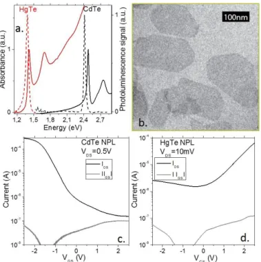
exchange, the optical features of the CdTe NPL initially in the green shift toward near infrared, see Figure 2a. The obtained materials present a narrow PL of 55 meV for the entire measurement. For the sake of comparison, the other nanocrystal materials (PbS and CuGaInS(e) ) emitting in the same range of wavelength present a linewidth of 100 meV, even for single particle measurements. Another striking optical feature resulting from the 2D shape is the fast PL emission of these NPL. The PL decay has been determined to be around 60 ns. Due to the higher binding energy resulting from the 2D shape. The PL decay is typically 50 times faster than what can be obtained with PbS and CIGS,
Figure 2 a. Absorption spectra of CdTe and HgTe NPL. b. TEM image of HgTe NPL. c. Transfer curve (drain and gate current as a function of gate bias) for CdTe NPL film measured in an electrolytic transistor configuration at room temperature. d. Transfer curve for a film of HgTe NPL. Adapted from ref [5]
We further investigate the transport properties of these 2D NPL. To do so, we incorporate the NPL into an electrolytic transistor, where the gate is obtained by ion gel gating [21,22]. This geometry allows us to explore large carrier density injection thanks to gate capacitance in the range of some µF.cm-2 and in volume gating volume
[23]. To build the device, we first exchange the NPL ligands. The initial long capping ligands (oleylamine and oleic acid) are replaced by short S2- ions [24]. In a second step, the ion gel made of LiClO
4 in PEG is deposited on
the top of the film. The initial CdTe NPL present a p-type behavior, see Figure 2c whereas after the cation exchange, the HgTe NPL become n-type, see Figure 2d.
To further explore the infrared properties of CQD and push their absorption toward longer wavelength, an interesting approach is to switch from interband transition in narrow band gap material to intraband transition. To observe intraband transition in CQD, some carrier(s) have to be injected within the conduction band. This can be obtained by optical pumping [25] or electrochemical injection [26]. However, these approaches remain poorly convenient for the design of device. Recently, self-doped CQD presenting mid infrared intraband absorption have been obtained with HgS [27] and HgSe [6,28]. We proposed an improved synthesis for HgSe with a wider range of size [6]. The typical absorption spectrum of the HgSe CQD presents two main contributions. In the near IR, we observe a broad absorption relative to interband absorption and in the mid and far infrared, we observe a peak relative to the intraband transition. Transport measurements, again conducted in an ion gel transistor configuration,
have confirmed this doping and demonstrate its n-type nature (ie electron doping) [6,29]. In this case we rather use As2S3 as capping ligand because of its low absorption in the mid infrared and also because of the previously
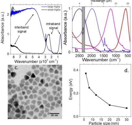
demonstrated capability of this ligand to generate high mobility and photoresponsivity [30,31]. We demonstrate the possibility to tune the HgSe CQD size from 4 to 50 nm while tuning the Se precursor (Se complexed with trioctylphosphine or SeS2), reaction duration and temperature (70°C-120°C). As a result, the intraband peak energy
can be tuned from 3 to 20 µm, see
Figure 3
b and d. The obtained material presents no aggregation, as shown on the TEM image, seeFigure 3
c.Figure 3 a. Absorption spectrum for two sizes of HgSe CQD. b. Zoom on the intraband contribution of the absorption spectra of HgSe CQD for four sized of HgSe CQD. c. TEM image of HgSe CQD. d. Energy dependence of the intraband transition as a function of the CQD size. Adapted from ref [6].
The origin of the self-doping was attributed to a reduction of the HgSe by its environment because of the large work function of the bulk [32] and limited interband band edge energy. This brings the conduction band below the O2/H2O redox couple and the negatively charged CQD becomes the stable form. We demonstrate that the doping
magnitude can be tuned by charging the capping ligands [29], we typically observe that the carrier density can be tuned by a factor 10 from 2 carriers per dot with dodecanetiol capping down to 0.2 carrier per dot with S2- capping
ions.
CONCLUSION
Significant progress has been obtained on the synthesis of mercury chalcogenides CQD with infrared optical absorption. Since the early nanocrystals absorbing above 3 µm in 2011, 2D materials have been proposed and synthetized with a strategy to achieve narrower optical features. Compared to previously existing nanocrystals, the 2D NPL of HgTe have enhanced PL performances with PL a narrower, faster and greater efficiency (about 10%). Concerning the mid infrared absorption, the synthesis of self-doped nanocrystals made of HgS and HgSe, have for the first time allows the observation of intraband features in the mid IR. It addresses the atmospheric transparency window, without the constrain of optical or electrochemical pumping. This interband absorption is tunable up to the THz range. The possibility to use intraband transition opens new possibilities for the design of infrared CQD based device.
ACKNOWLEDGEMENTS
This work was supported by French state funds managed by the ANR within the Investissements d'Avenir program under reference ANR-11-IDEX-0004-02, and more specifically within the framework of the Cluster of Excellence MATISSE led by Sorbonne Universités. SI thanks the ANR for funding through the Nanodose grant.
REFERENCES
[1] D.V. Talapin, J.S. Lee, M. Kovalenko, E. Shevchenko, “Prospects of Colloidal Nanocrystals for Electronic and Optoelectronic Applications”, Chem. Rev. 110, 389 (2010).
[2] A. Rogalski, J. Antoszewski, L. Faraone, “Third-generation infrared photodetector arrays”, J. Appl. Phys. 105, 091101 (2009)
[3] S. V. Kershaw, A. S. Susha, A. L. Rogach, “Narrow bandgap colloidal metal chalcogenide quantum dots: synthetic methods, heterostructures, assemblies, electronic and infrared optical properties,” Chem. Soc. Rev. 42, 3033 (2013).
[4] E. Lhuillier, S. Keuleyan, H. Liu, P. Guyot-Sionnest “ Mid-IR Colloidal Nanocrystals”, Chem Mat. 25, 1272 (2013) [5] E. Izquierdo, A. Robin, S. Keuleyan, N. Lequeux, E. Lhuillier, S. Ithurria, “Strongly confined HgTe 2D nanoplatelets as narrow near infrared emitter” J. Am. Chem. Soc. 138, 10496 (2016).
[6] E. Lhuillier, M. Scarafagio, P. Hease, B. Nadal, H. Aubin, X. Z. Xu, N. Lequeux, G. Patriache, S. Ithurria; B. Dubertret, “Infrared photo-detection based on colloidal quantum-dot films with high mobility and optical absorption up to the THz” Nano
Lett 16, 1282 (2016).
[7] M.V. Kovalenko, E. Kaufmann, D. Pachinger, J. Roither, M. Huber, J. Stangl, G. Hesser, F. Schaffler, W. Heiss, “Colloidal HgTe nanocrystals with widely tunable narrow band gap energies: from telecommunications to molecular vibrations” J. Am.
Chem. Soc. 128, 3516 (2008).
[8] E. Lhuillier, S. Keuleyan, P. Guyot-Sionnest, “Optical properties of HgTe colloidal quantum dots”, Nanotechnology 23, 175705 (2012).
[9] G. Allan, C. Delerue, “Tight-binding calculations of the optical properties of HgTe nanocrystals,” Phys. Rev. B 86, 165437 (2012)
[10] S. Keuleyan, E. Lhuillier, V. Brajuskovic, P. Guyot-Sionnest, “Mid-infrared HgTe colloidal quantum dot photodetectors”
Nat Photon. 5, 489, 2011.
[11] E. Lhuillier, S. Keuleyan, P. Rekemeyer, P. Guyot-Sionnest, “Thermal properties of mid infrared Colloidal quantum dot detectors” J. Appl. Phys 110, 032110 (2011).
[12] S. Keuleyan, E. Lhuillier, P. Guyot-Sionnest, “Synthesis of Colloidal HgTe Quantum Dots for Narrow Mid-IR Emission and Detection” J. Am. Chem. Soc. 133, 16422 (2011).
[13] S. E. Keuleyan, P. Guyot-Sionnest, C. Delerue, G. Allan, “Mercury Telluride Colloidal Quantum Dots: Electronic Structure, Size-Dependent Spectra, and Photocurrent Detection up to 12 μm” ACS Nano 8, 8676, (2014).
[14] S. Ithurria, B. Dubertret, “ Quasi 2D Colloidal CdSe Platelets with Thicknesses Controlled at the Atomic Level”, J. Am.
Chem. Soc. 130, 16504 (2008)
[15] M. Nasilowski, B. Mahler, E. Lhuillier, S. Ithurria and B. Dubertret, “2D Colloidal nanocrystals” Chem. Rev.,116, 10934 (2016)
[16] E. Lhuillier, S. Pedetti, S. Ithurria, B. Nadal, H. Heuclin and B. Dubertret, “2D Colloidal Metal Chalcogenides Semiconductors: Synthesis, Spectroscopy and Applications” Acc. Chem. Res. 22, 48, (2015).
[17] S.Pedetti, B. Nadal, E. Lhuillier, B. Mahler, C. Bouet, B. Abécassis, X. Xu, B. Dubertret, “Optimized Synthesis of CdTe Nanoplatelets and Photoresponse of CdTe Nanoplatelets Films”, Chem. Mat 25, 2455 (2013).
[18] L. De Trizio, L. Manna, “Forging Colloidal Nanostructures via Cation Exchange Reactions”, Chem. Rev., 116, 10852 (2016).[19] D.H. Son, S.M. Hughes, Y. Yin, A.P. Alivisatos, “Cation exchange reactions in ionic nanocrystals”, Science. 306, 1009 (2004).[20] B. J. Beberwyck, Y. Surendranath, A.P. Alivisatos, “Cation Exchange: A Versatile Tool for Nanomaterials Synthesis”, J. Phys. Chem. C 117, 19759 (2013).[21] E. Lhuillier, S.Pedetti, S. Ithurria, H.Heuclin, B. Nadal, A. Robin, G. Patriarche, N. Lequeux, B. Dubertret, “Electrolyte Gated Field Effect Transistor to Probe the Surface Defects and
Morphology in Films of Thick CdSe Colloidal Nanoplatelets” ACS Nano 8, 3813 (2014).
[22] E. Lhuillier, A. Robin, S. Ithurria, H. Aubin, B. Dubertret, “«Electrolyte gated colloidal nanoplatelets based phototransistor and its use for bicolor detection” Nano Lett. 14, 2715 (2014).
[23] E. Lhuillier, S. Ithurria, A. Descamps-Mandine, T. Douillard, R. Castaing, X.Z. Xu, P-L. Taberna, P. Simon, H. Aubin, B. Dubertret, “Investigating the n and p type electrolytic charging of colloidal nanoplatelets“, J Phys Chem C 119, 21795 (2015) [24] A. Nag, M. V. Kovalenko, J.-S. Lee, W. Liu, B. Spokoyny, D.V. Talapin. Metal-free Inorganic Ligands for Colloidal Nanocrystals: S2–, HS–, Se2–, HSe–, Te2–, HTe–, TeS
32–, OH–, and NH2– as Surface Ligands, J. Am. Chem. Soc. 133, 10612
(2011).[25] K. S. Jeong and P. Guyot-Sionnest, “Mid-Infrared Photoluminescence of CdS and CdSe Colloidal Quantum Dots,”
ACS Nano 10, 2225 (2016).
[26] M. Shim and P. Guyot-Sionnest, “N-type colloidal semiconductor nanocrystals,” Nature 407, 981 (2000).
[27] K. S. Jeong, Z. Deng, S. Keuleyan, H. Liu and P. Guyot-Sionnest, “Air-Stable n‑Doped Colloidal HgS Quantum Dots” J.
Phys. Chem. Lett. 5, 1139 (2014).
[28] Z. Deng, K.S. Jeong, P. Guyot-Sionnest “Colloidal Quantum Dots Intraband Photodetectors”, ACS Nano 8, 11707 (2014).
[29] A. Robin, C. Livache, S. Ithurria, E. Lacaze, B. Dubertret, E. Lhuillier, “Surface Control of Doping in self-doped Nanocrystals” ACS Appl. Mat. Interface 8, 27122 (2016).
[30] E. Lhuillier, S. Keuleyan, P. Zolotavin, P. Guyot-Sionnest “Mid-Infrared HgTe/As2S3 FETs and photodetectors” Adv. Mat.
25, 137 (2013).
[31] S. Yakunin, D.N. Dirin, L. Protesescu, M. Sytnyk, S. Tollabimazraehno, M. Humer, F. Hackl, T. Fromherz, M.I. Bodnarchuk, M.V. Kovalenko, W. Heiss, “High Infrared Photoconductivity in Films of Arsenic-Sulfide-Encapsulated Lead-Sulfide Nanocrystals”, ACS Nano. 8, 12883 (2014).
[32] A. H. Nethercot, Jr. “Prediction of Fermi Energies and Photoelectric Thresholds Based on Electronegativity Concepts”
![Figure 1 a TEM image of early HgTe nanocrystals with absorption edge reaching the 3-5 µm range, adapted from ref [10] b is the associated absorption spectrum with a broad absorption edge resulting from the limited size control](https://thumb-eu.123doks.com/thumbv2/123doknet/14511640.529819/3.892.107.766.275.663/nanocrystals-absorption-reaching-associated-absorption-spectrum-absorption-resulting.webp)