Construction of a Superconducting Circuit Simulator
and its Applications in Cryogenic Computing
by
0. Murat Onen
Submitted to the Department of Electrical Engineering and Computer
Science
in partial fulfillment of the requirements for the degree of
Master of Science in Electrical Engineering and Computer Science
at the
MASSACHUSETTS INSTITUTE OF TECHNOLOGY
February 2019
@
Massachusetts Institute of Technology 2019. All rights reserved.
Author
Signature redacted
Department of Electrical Engineering and Computer Science
January 31, 2019
Cetfidby.Signature
redacted
Certified by..
(UO
Karl K. Berggren
Professor of Electrical Engineering and Computer Science
Thesis Supervisor
Accepted
MASSACHUSETTS INSTITUTE OFT ECHNOLOGYFEB
21
2019
L
LIBRARIES
by
..
...
Signature redacted
X",
/ 1
F 1* A 17 1 1I
_, Leslie A. KOlOdZ1ejSKiProfessor of Electrical Engineering and Computer Science
Chair, Department Committee on Graduate Students
Construction of a Superconducting Circuit Simulator and its
Applications in Cryogenic Computing
by
0. Murat Onen
Submitted to the Department of Electrical Engineering and Computer Science on January 31, 2019, in partial fulfillment of the
requirements for the degree of
Master of Science in Electrical Engineering and Computer Science
Abstract
In this work, I first construct a unified simulation platform, where superconducting electronics can be designed and optimized with high performance and accuracy. For this purpose, I first select numerical simulation methods that can deal with the highly non-linear characteristics of the superconducting devices. I validate the simulated re-sponses with experimental data on device and circuit level examples. Following the implementation of the simulator, I use this framework to analyze existing supercon-ducting nanowire based technologies, and optimize them for wider operation regimes and higher performance metrics. I use nanofabrication processes to realize these devices and conduct liquid helium immersion measurements to characterize them ex-perimentally. Optimized devices show superior characteristics that demonstrate the predictive capabilities of this simulator. Finally, I use this simulator to design a su-perconducting nanowire based deep neural network training accelerator. I design, implement, and characterize a unit cell for this application. These local processors have significant device-level advantages over the readily available non-volatile memory technologies in realizing mixed-signal architectures. The devices produced through-out this work have immediate and near-term applications, proving the merit of having a high-performance simulator.
Thesis Supervisor: Karl K. Berggren
Acknowledgments
The study reported in this thesis would not have been possible without the support and advice of my colleagues, family and friends. In particular, I would like to thank:
My advisor, Prof. Karl K. Berggren, for his insight, dedication to science and
pro-viding a nourishing environment for his students in building independent researching skills. His method of following a wide spectrum of research has initiated and greatly supported this work throughout its course.
Andrew E. Dane, for being my mentor in the field and teaching me the fundamen-tals of material science, nanofabrication, and even more importantly, scientific rigor. Most of this work would have got stuck on an idea level if he had not chosen to share his knowledge and experience with me.
Brenden A. Butters, Emily Toomey, Marco Colangelo, Di Zhu, and Eugenio Mag-giolini for their helpful discussions, collaborations and experimental assistance.
Tayfun Gokmen, Wilfried Haensch and Heike Riel at IBM T.J. Watson Research Center, for giving me the first opportunity to become a part of something bigger.
Prof. Luca Daniel for teaching me advanced numerical simulation techniques that I have used extensively in this work.
Dorothy Fleischer for her kindness, generosity and help with keeping the group organized.
Mark Mondol, James Daley and Kurt Broderick for their technical support with fabrication.
Marco Turchetti for being a true friend and a very professional colleague who has widened my view on a long list of subjects.
My dearest colleague, Sila Deniz Calisgan, for bringing joy, laughter and
excite-ment in my life. I feel very fortunate for having been able to share all the moexcite-ments of this adventure with her.
My parents, and both grandfathers, who are the very reason behind my
determi-nation. I am grateful for their unconditional trust and encouragement. None of this work could be possible if it weren't for their dedication.
Contents
1 Introduction
1.1 Fundamental Properties of Superconductors . . . .
1.2 Small Superconductors . . . .
1.3 Superconducting Nanoelectronics and Cryogenic Computing
1.3.1 T hesis goal . . . .
1.3.2 Thesis outline . . . .
2 Construction of the Superconducting Circuit Simulator
2.1 Introduction to Superconducting Devices . . . . .
2.1.1 Josephson Junctions . . . .
2.1.2 Superconducting Nanowire Based Devices
2.2 Superconducting Circuit Simulators . . . .
2.2.1 Simulation Framework . . . .
2.2.2 Phase Coherent Circuit Solver . . . .
2.2.3 Classical Circuit Solver . . . .
2.2.4 Dynamic Time-Stepping . . . .
2.3 Demonstrations and Performance Analysis . . . .
3 Optimizing Layout and Material Considerations ing Nanowire-Based Electronics
. . . . 19 . . . . 19 . . . . 21 . . . . 26 . . . . 27 . . . . 28 . . . . 30 . . . . 32 . . . . 34
for
Superconduct-3.1 Superconducting Nanowire Based Memory (nMEM) . . . . 3.1.1 Fundamental Operation of Superconducting Nanowire Memory 3.1.2 Unconventional Operation Modes of the nMEM . . . . 39 40 40 45 13 . . 13 . . 14 . . 15 . . 16 . . 16 193.1.3 Operation Margins of the nMEM . . . . 46
3.1.4 Optimization of Superconducting Nanowire-Based Memory . . 47
3.1.5 Fabrication of Superconducting Nanowire-Based Memory . . . 51
3.1.6 Experimental Characterization of Superconducting Nanowire-Based M em ory . . . . 53
3.2 Multi-level Flux Shuttling with Shunted Nanowires . . . . 55
3.2.1 Fundamental Operation of Shunted Nanowires . . . . 56
3.2.2 Simulator Validation with Prior Experimental Results . . . . . 60
3.2.3 Optimization of Shunted Nanowires . . . . 63
3.2.4 Fabrication of Optimized Shunted Nanowires . . . . 66
3.2.5 Experimental Characterization of Optimized Shunted Nanowires 70 4 Design of a Superconducting Deep Neural Network 'Fraining Accel-erator 75 4.1 Introduction to Deep Neural Networks (DNNs) . . . . 75
4.1.1 Fundamentals of Deep Neural Networks . . . . 76
4.1.2 Crossbar Architecture . . . . 77
4.1.3 Crosspoint Element Requirements . . . . 79
4.2 Superconducting Nanowire-Based Processor . . . . 80
4.2.1 State Representation and Programming . . . . 80
4.2.2 Analog Multiplication . . . . 82
4.2.3 Crossbar Architecture and Operation . . . . 84
4.2.4 Simulation Results for Superconducting Nanowire-Based Pro-cessor . . . . 86
4.2.5 Design and Fabrication of Unit Cell . . . . 87
4.2.6 Experimental Characterization of Superconducting Nanowire-Based Inductive Processing Unit . . . . 89
4.2.7 Discussions for Superconducting Nanowire-Based DNN Train-ing Accelerator . . . . 90
List of Figures
2-1 RCSJ model and IV characteristics of a shunted Josephson junction. 20
2-2 Circuit schematic of an SFQ logic NAND gate. . . . . 22
2-3 Simulated IV characteristics of shunted and unshunted superconduct-ing nanow ires. . . . . 34
2-4 Experimental and simulated IV characteristics of a shunted Josephson junction . . . . 35
2-5 Simulated response of an SFQ logic NAND gate. . . . . 36
2-6 Circuit schematic of an SFQ logic AND gate . . . . 37
2-7 Simualted responce of an SFQ logic AND gate . . . . 37
2-8 Simulated response of a 3-bit SFQ logic counter . . . . 38
3-1 Circuit schematic of a superconducting nanowire memory (nMEM). . 41 3-2 Simulated response of an nMEM device. . . . . 44
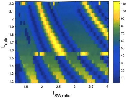
3-3 Optimization of nMEM. . . . . 49
3-4 Performance of nMEM with respect to the cross-swept ISW,ratio and Lratio. 50 3-5 Micrographs of the optimized and unoptimized nMEM devices. ... 52
3-6 Experimental characterization of optimized and unoptimized nMEM devices. . . . . 54
3-7 Simulated response of shunted and unshunted nanowires. . . . . 58
3-8 Simulated response of operation of a shunted nanowire in controlled flux shuttling. . . . . 60
3-9 Prior experimental data of controlled flux shuttling with a shunted nanow ire. . . . . 61
3-10 Simulated response validation with the formerly characterized shunted
nanowire operation. . . . . 63
3-11 Flux-per-event metric of a shunted nanowire cross-swept for the shunt
inductor, shunt resistor and loop inductor. . . . . 64
3-12 Simplified fit for flux-per-event metric of a shunted nanowire
cross-swept for the shunt inductor, shunt resistor and loop inductor. .... 65
3-13 Simulated repsonse for a shunted nanowire with differnt thermal
sink-ing characteristics. . . . . 65
3-14 Micrographs of failed fabrication attempts. . . . . 69
3-15 Snapshots of the optimized shunted nanowire chip at different process
steps... ... 71
3-16 Experimental characterization of IV curves for nanowires with different
shunting properties. . . . . 72
3-17 Experimental characterization of controlled flux shuttling with
opti-mized shunted nanowires. . . . . 74
4-1 Schematics of a resistive crossbar array at different steps of backprop-agation. . . . .
...78
4-2 Fundamental operation of the superconducting nanowire-based
cross-point elem ent. . . . . 81
4-3 Analog multiplication scheme for superconducting nanowire based
pro-cessor. . . . . 83
4-4 Circuit schematic for a superconducting nanowire-based crossbar array. 84 4-5 Simulated response of the superconducting nanowire-based processor
in incremental state programming. . . . . 87
4-6 Micrograph and basic experimental characterizations of a
supercon-ducting nanowire-based cross-point element. . . . . 88
4-7 Experimental characterization of the state programming and analog multiplication of the superconducting nanowire-based cross-point
List of Tables
2.1 Performance metrics of the simulator, derived from SFQ logic device
sim ulations. . . . . 37
3.1 Circuit parameters used in prior experimental characterization of shunted
nanow ires. . . . . 62
3.2 Physical parameters used for the simulation of the shunted nanowires 62
Chapter 1
Introduction
1.1
Fundamental Properties of Superconductors
The resistance of a normal metal gradually decreases as the temperature is lowered
and saturates at very low temperatures1 . However, some metals, undergo a phase
transition to the superconducting state (zero resistance), below a critical temperature
(T). Some typical T values for elemental superconductors are; 9.25 K for niobium,
1.1 K for aluminum and 7.1 K for silicon under high pressure
131.
For transition metalcuprate compounds T values of >120 K have been reported while the record is being
held by H2S with 203K (at ~ 150 GPa) [131.
In addition to the perfect conductivity, superconductors exclude magnetic flux. This perfect diamagnetism is named as the Meissner effect and can be used to dif-ferentiate a perfect electrical conductor and a superconductor. Similar to a critical temperature, there exists a critical magnetic field (Hc) where the phase transition occurs. Typical values for He can be given as 198 mT for niobium and 9.9 mT.
As a consequence of perfect conductivity, if a current is somehow injected into a superconducting loop, it continues to flow indefinitely. This property is also limited by a current carrying capacity, known as the critical current density (Jc). Interestingly,
the resulting flux due to these currents is found to be quantized in units of D, = 2eh . In
this work, these phenomena of 'digitized persistent currents' will be used extensively
in Chap.3 and Chap.4.
The aforementioned quantization effect indicates that superconductivity is a macro-scopic quantum mechanical phenomenon. This has been followed by a description of superconductivity where all of the superconducting electrons are represented by a single wave function. According to the BCS theory of superconductivity, physical mechanisms behind these effects lie in the pairing of the fermionic particles to form a Bose gas of paired quasiparticles. This process is mediated by electron-phonon cou-pling and results in the creation of Cooper pairs [10]. The reasoning of such a pairing can be (over)simplified by using minimizing Hamiltonian argument.
The full description of superconductivity deserves an extensive explanation of the physics. For the sake of conciseness, we will skip most of these curious phenomena such as the superconducting energy gap, quasi-particle tunneling, supercurrent equa-tion, the two-fluid model, vortex phases and flux pinning. Instead, we will skip to explaining some of the phenomena and terminology that are of particular importance for the work conducted in this thesis. The reader can use the following references for detailed coverage of the superconductivity: Refs.[42, 331. The author also wants
to cite the lecture notes prepared for the MIT course 6.732 by Prof. Mildred S.
Dresselhaus, which are also extensively used in the preparation of this introductory chapter.
1.2
Small Superconductors
Small superconductors refer to superconducting objects with scales smaller than the characteristic lengths of such materials in one or more dimensions [32]. These fun-damental length scales are the magnetic penetration depth A [28], and the coherence length [17]. Former defines the extent of the magnetic field can penetrate into the superconductor while the later indicates the spatial extent over which the supercon-ductivity does not get affected by any local perturbations (e.g. thermal fluctuations). In this work, we have worked with thin film superconductors of thicknesses varying between 5-30 nm. In such dimensions, it is known that the film's surface and interface
confine the motions of the electrons, leading to the formation of quantum well states
[8]. These states heavily influence the overall electronic structure, density of states,
and the surface energies.
Understanding these length-scales and the resultant effects have been fundamen-tal for the work conducted in this thesis. For example, the coherence length plays a major role in the switching characteristics (hot-spot dynamics) of a superconduct-ing nanowire. Although we do not cover them in this work, vortex ratchets and flux pinning devices make use of magnetic penetration depth as well. As can be ex-pected, capturing these effects in our simulator will be fundamental in explaining the superconducting device characteristics.
1.3
Superconducting Nanoelectronics and Cryogenic
Computing
Following the prediction of tunneling possibility of superconducting Cooper pairs in a superconductor-normal-superconductor (SNS) system, superconducting electron-ics have been in the focus of research enabling a variety of novel applications in both analog and digital electronics. These applications can be exemplified as super-conducting quantum interference devices (SQUIDS), millimeter-wave mixers, voltage standards, high energy magnets, power transmission lines, and most importantly high-performance computing systems [37].
In the absence of phonon scatterings at the cryogenic temperatures, electron trans-port becomes ballistic. This in return allows the superconducting phase information to be preserved over longer times, that is used as the main method of information en-coding in quantum computational systems. In combination with the advancements in superconducting logic families such as single flux quantum (SFQ/RSFQ and eSFQ), reciprocal quantum logic (RQL) and adiabatic quantum flux parametron (AQFP)
[41], advantages of Josephson switching devices have been utilized more and more extensively in computing.
In addition to being uniquely situated for quantum computing approaches with their long coherence times, superconducting electronics also have innate character-istics that make them suitable for conventional electronics. The energy spent per switching can be as low as a fraction of an aJ with switching speeds on the order of hundreds of GHz.
Considering the unique and multidimensional physics of superconductors, com-plicated highly non-linear behavior of devices and demanding nanofabrication tech-niques, producing a fully-functional superconducting electronics chip can be im-mensely expensive. To make the field feasible to compete with conventional electron-ics and allow it to prevail in niche applications of computation, advanced simulation capabilities is an indisputable necessity.
1.3.1
Thesis goal
The main goal of this thesis work is to construct a unified simulation platform where superconducting electronics can be designed and optimized with high accuracy and performance. The simulator will be optimized to be able to deal with the strong non-linearity of superconducting switching elements and will include a variety of physical
disciplines such as quantum mechanics (e.g. flux quantization), thermodynamics
(e.g. hot-spot formation and dissipation) and electrical characteristics. Following the verification of the predictive capabilities of the framework, layout and material considerations will be optimized for existing applications. Finally, a novel application will be presented in the heavily researched deep neural network training field, fully exploiting the potential of superconducting nanowire-based devices.
1.3.2
Thesis outline
Chapter 2 - Construction of the Superconducting Circuit Simulator
The physical phenomena behind the Josephson junctions and the superconducting nanowires will be analyzed. Models of these devices will be incorporated in a simulator that uses advanced numerical techniques to obtain a high-performance and accuracy designing platform. Numerical problems that arise due to the strong non-linearity of the superconducting devices will be analyzed and mitigation techniques will be provided. Validation of the simulated responses will be made by comparisons with experimental data in device and circuit levels.
Chapter 3 - Optimizing Layout and Material Considerations for
Supercon-ducting Nanowire-Based Electronics
The simulator will be used to explain the behavior of two superconducting nanowire-based systems, a nanowire memory, and controlled flux shuttling. Operation margins of the nanowire memory will be derived and its sensitivity will be analyzed with respect to its circuit model parameters. Nanowire memories will be optimized for having wider operation margins. These optimal devices are then fabricated using nanofabrication techniques and experimentally characterized in liquid helium immer-sion measurements. Optimization results obtained by the software will be validated with these experimental results.
Secondly, the software will be used to better understand the controlled
flux-shuttling dynamics of shunted nanowires. Simulated responses will be compared
with former experimental characterizations as validation. Then, shunted nanowires are optimized by changing material stacks that involve higher thermal sinking of the nanowire, suggested by the simulator we have built. Such devices are realized again by using nanofabrication techniques and measured similarly in liquid helium dewar. Experimental characterization of these optimized shunted nanowires will show supe-rior characteristics which will be used as a basic element in the realization of the system we propose in Chap.4.
Chapter 4
-
Design of a Superconducting Deep Neural Network Training
Accelerator
The simulator built in this work is finally used in creating a novel application field for the superconducting nanoelectronics, mixed-signal accelerators for deep neural network training. A quick review of DNN fundamentals and crossbar architecture will be provided. Then, the conventional resistive crossbar will be adapted into a superconducting nanowire-based alternative version. This approach mitigates the foregoing problem with the classical non-volatile memory approaches by providing inherently suitable physical characteristics for the application. A cross-point element will be fabricated, making use of the optimized shunted nanowires we have designed in Chap.3.2.3. Experimental characterization of the unit cell will be presented with an overview of system level requirements to realize a full-scale implementation.
Chapter 2
Construction of the Superconducting
Circuit Simulator
2.1
Introduction to Superconducting Devices
Superconducting devices that this work will include are Josephson junctions (JJs) and superconducting nanowire (SCNW) based devices. Having very different dynam-ics and operational principles increase the capability of superconducting electrondynam-ics solutions when interfaced in hybrid designs. This chapter will discuss the physical foundations of these devices and give proper modeling of them.
2.1.1
Josephson Junctions
Josephson junctions can be defined as a tunneling device, using Cooper pairs as the charge carriers. They are realized by sandwiching a barrier layer in between
two superconducting layers. If this barrier is sufficiently thin
(~
few nanometers),the superconducting wavefunction (describing the probability of finding a Cooper pair) can tunnel through this insulating layer. The super-current (Josephson current) flowing through the device is described with the Josephson equation given below:
'Y = 2 - #1 - AdI, (2.2)
where q is the phase of the macroscopic wave function, -y is the gauge invariant phase
difference between the two superconductors and I, is the critical current of the device
[21]. When a direct voltage V is applied to this stack, -y varies as a function of time
as follows:
-=
-
e
(2.3)
dt
h'
where e is the charge of an electron and h is the Planck constant [22]. As can be
seen from the Eq.2.1, the current-voltage characteristics of the Josephson junctions
are highly nonlinear.
(a)
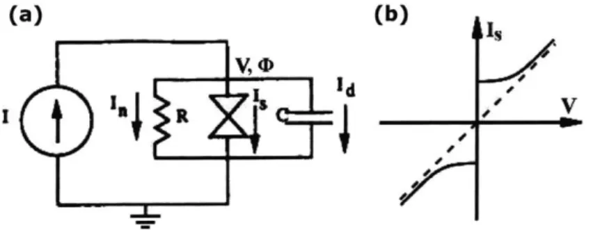
(b)
IS
R.
V
94 0
Figure 2-1: RCSJ model for a shunted Josephson junction and its characteristic
non-hysteretic current-voltage relation. Figure modified from Ref. [22].
RCSJ Model of Josephson Junctions
A common way to describe the behavior of the Josephson junction is its
alterna-tive circuit model: Resisalterna-tive-Capacialterna-tively-Shunted junction (RCSJ). Using the RCSJ
model shown in Fig.2-1, Josephson junctions can be described by using the following
constitutive equations Eq.2.4 and Eq.2.5, where I, R and C are device parameters
and # is the phase difference of superconducting order parameter 9 between the two
terminals of the junction [22]:
I Is + In + Id=
Icsin(#) +
h
+
2 (2.4)2eR dt 2e dt2
V .
h(2.5)
2e dt dt
In steady state, this behavior can be linearized as: D = LjOI, where 1 = h#\2e,
Ljo = h\2eIc, and
#
is the superconducting wavefunction phase. Therefore, JJs can be modeled as inductors if the phase is used as the nodal quantity and current as branch quantity.SFQ Logic Gates
The dominant superconducting integrated circuit technology involving the implemen-tation of Josephson junctions is single flux quantum (SFQ) logic. This technology uses arrangements of inductors and JJs to perform complex computation at clock rates beyond 20 GHz [37]. The inputs and outputs of the SFQ systems are fast voltage pulses that represent logic states, which have the integral of, as the name suggests, a
single flux quantum which is (% = h\2e = 2.067 833 831 fWb.
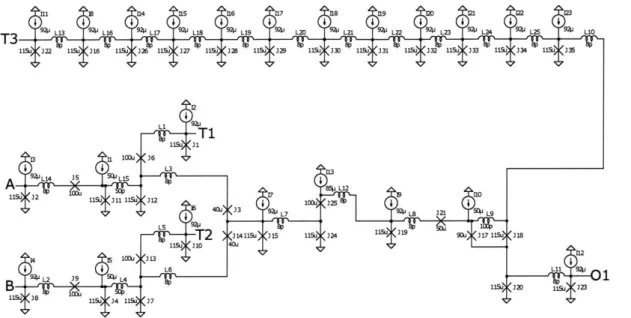
Fig.2-2 illustrates a sample SFQ logic based NAND gate consisting of 23 current sources, 25 inductors, and 35 JJs. The circuit is constructed as an AND gate (bottom left) followed by a NOT gate (bottom right), where the top part is basically a delay line, namely a Josephson Transmission Line (JTL), for the clock signal to arrive at the NOT gate at the same time as AND output. The schematic also includes circuitries that give directionality to the SFQ signal (e.g. J24-J25). These valve structures avoid bleeding of the output signal back to the circuit instead of getting transmitted to the next stage. As will be shown in Sec.2.3 this circuit can be clocked at 500GHz where the output follows the input with one clock cycle delay.
2.1.2
Superconducting Nanowire Based Devices
Nanowire-based devices can be considered as the second main family of superconduct-ing electronics. The main operation of these devices is obtained through switchsuperconduct-ing
il 1B 114 15 116 117 n8 19 22 21 22 23
1 1 1 4 ' 4 4 4 4 4 4 1
T3 92p L13 9 L16 92' L17 2? L 2 19 p L2 92 L21 L22 92P L23 L24 1L25 L10 113 122 115u J16 115U 126 11W 327 114 123 115u J29 115U 130 112U J31 1124 132 112u J33 11M J34 112J J23
L1 115u
31
B 1M0U J6 92pW L14 J L15 L3U A- )8- L12 115U o2 1 2115 J12 nouJ2 B 41 4Du J3 927 L8 J21 M L9 L5 2 _J J '1411Mu JIs 115uo J24 1150 019 jig37119 1 1 J10 40u 14 15 10ou 313 U L18 011 J81 4 11 u L11 9%p19;
Figure 2-2: Example SFQ logic based NAND gate implementation. High device
count is mainly due to the transmission line (top branch) working as delay elements
to satisfy pulse timing requirements.
these devices (from the superconducting state to resistive state). These switching
events are thermally mediated by the growth of a region, often called as a
hot-spot. The growth of these hot-spots is initiated once the current through the device
exceeds the switching current of the device. On the other hand, the decay of the
hot-spot occurs at lower than this threshold due to Joule-self heating. In other words,
the switching characteristics of these devices are hysteretic.
The switched (i.e. normal, resistive) region in a nanowire has high electrical
impedance. Therefore, they can potentially fan out to many devices. This property
has allowed these devices to perform as interfaces between JJ based circuits and
CMOS architectures
[481.
However, thermal breakdown of the superconductivity
prevents these devices from supporting quantum coherent transport. This behavior
is expected as the switching event is essentially a burst of phonons that scrambles the
phase information. Furthermore, again due to their thermal characteristics, switching
frequencies of nanowire-based devices are lower than the JJs.
The most basic structure in this device family is a nanowire constriction
1. A
'Note that in Chap.3 and Chap.4, we sometimes refer to this constriction geometry as simply nanowire and use the term interchangeably.
nanowire constriction is essentially a narrowing in a nanowire, that has a reduced
switching current2 relative to the surrounding region. As mentioned above, exceeding
this threshold leads to hot-spot growth in this constricted region. The area difference between the constricted part and the rest ensures the hot-spot event to occur reliably in a well-defined region. Once the hot-spot blocks the entire cross-section of the
nanowire, the device is called to be switched into the normal (resistive) state3 .
The nanowire constriction can be interpreted as a linear resistor and a non-linear inductor as a function of current passing through it. The resistance of the constriction is related to the hot-spot through the simple linear relation given below:
p1
RHS = --
(2-6)
dw'
where p and d are the resistivity and thickness of the superconducting film, w is the constriction width and 1 is the hot-spot length.
The rate at which the spot size changes (growth or decay) is called the hot-spot velocity. The hot-hot-spot velocity is dependent on the current flowing through the nanowire in a hysteretic relation. Nucleation of it only occurs once the current flowing through the device exceeds its switching current. Once it forms, its growth/decay
depends on whether the Joule heating (oc 12R) or the cooling is more dominant.
As a definition, the current at which the hot-spot neither grows nor decays is called
as the hot-spot current IHs or the retrapping current IR. Note that this current is
roughly one-fifth of the switching current (for thin film NbN devices on an insulating substrate), giving rise to the hysteretic current-voltage relation of the nanowire-based devices. The equation for the hot-spot velocity (vHS) is given as following:
dl 4'ilw\sw -2
VHS --
2v
0(2.7
dt
V/'0_jNw
\ Is2W- _where vo is the characteristic velocity and
4'
is the Stekly parameter [231. These terms2Here we choose to use the term switching current instead of the critical current to account for all the possible suppression effects over the depairing current.
'Before this point current flowing in the wire can bypass the hot region and flow around. The device response does not change until the device is switched into the normal state as the supercon-ducting part short-circuits the rest before.
can be written in terms of material and environment parameters as:
vo h ,\d (2.8)
C
= PIsw (2.9)
hew2d(Tc -
Ts)'
where K is the thermal conductivity of the nanowire, he is the thermal contact con-ductivity, c is the specific heat per unit volume of the nanowire and Tc,s are the temperatures of the constriction and the substrate respectively.
Considering that the nanowire is constricted only for a limited extent, 1
Hs has to
be less than or equal to the Xconstriction, which is the physical length of the constriction.
On the other hand, the minimum size of a hot-spot is given by the coherence length ( of the material. This length is a function of temperature as given below:
( (0)
((T) = . (2.10)
For the sake of simplicity, we will ignore this effect of temperature change around the hot-spot region.
As can be inspected from 2.7, vHS diverges as the denominator approaches to
0. This creates a mathematical instability for modeling nanowire behavior as each
switching event involves that particular point. The simplest solution is to saturate this velocity at a certain level. This approach makes physical sense as well considering that the hot-spot decay (a thermal cooling event) cannot occur at an arbitrarily fast rate (i.e. faster than the phonon escape time). In order to pick the fastest rate, we
use the hot-spot size a heat capacity, as it is the over time integration of VHS. Then,
we assume an exponential decay and modify 2.7 as follows:
vHS = max(vH HS) (2.11)
Tth
where IHS is the hot-spot size at that time instance.
with a load attached to the nanowire can be described as: (1) switching ('NW
f-Isw), (2) current redirection until growth stops ((INw ~~ IR)), (3) decaying and
,final
eventually diminishing of the hot-spot (f.NW dvHs < ( ). The final current in
the nanowire at the end of the switching event is therefore determined by: (1) the electrical time constants that determine the rate of change in the current flowing through the nanowire and (2) the thermal time constants that determine how fast hot-spot events can take place. Chapter 3.2 will further discuss the methods and results of modifying these characteristic timescales. Furthermore, one can find a more thorough analysis of modeling nanowire-based devices in Ref.141.
Most importantly, as the devices are purely classical (i.e. not operated with quan-tum mechanical principles), the modeling of them can be done with a simple circuit model. In other words, unlike JJs described in Sec.2.1.1, the evolution of phase across the device can be neglected. This factor allows us to apply model order reduction and simplifies the numerical complexity of the system significantly.
Here we want to note that the aforementioned devices make use of a phenomenon called the kinetic inductance[2]. Similar to the conventional definition of self-inductance
L in a circuit that is associated with the energy stored in the magnetic field produced
by the electrical current, the kinetic inductance, Lk, can be defined as the
mecha-nism that stores energy directly related to the motion of the charge carriers. For an electron, the motion equation can be written as:
dv -v = -qE - -(2.12)
v-dt m. T
where m is the mass (9.1094 x 10⁻²⁸ g) and q is the charge of an electron (1.6022 x
10-19 C). Writing the same equation in terms of the current density J = -qnv:
m m dJ dJ
E = (n)J+(
) =pJ+
A--.
(2.13)
q2n T e2 dt
dt
II
As can be seen from Eq. 2.13, the very motion of the electron gives rise to an effect that can be interpreted as an additional inductive behavior with kinetic inductivity
superconductors due to the zero series DC resistance [22]. This property will be used extensively in Chapters 3 and 4 in designing area-efficient large inductors.
Superconducting nanowires can be used for a variety of interesting applications. For example, the recently demonstrated nanowire cryotron (or nTron) [30], makes use of nanowire constrictions in its operation. Furthermore, in a y-shaped geometry, nanowire devices can utilize the current crowding effect for sensing applications (e.g. as a readout device alternative to SQUIDs)[29]. In this work, we will focus on two main examples to show the simulation and optimization capability of the simulator: (1) a nanowire memory (nMEM) in Sec.3.1, and (2) a shunted nanowire for controlled flux shuttling in Sec.3.2. These applications have been proposed previously in Ref. [491 and Ref. [43], where this work improves their characteristics using the software we build out of scratch. Finally, as a novel application, Chap.4 discusses the usage of superconducting nanowire-based devices in deep neural network training acceleration.
2.2
Superconducting Circuit Simulators
Computer-aided design (CAD) platforms for superconducting electronics have been of interest in the last three decades [34, 47, 16, 15]. The common main goal of these softwares is to create a high-performance design environment, similar to those of semiconductors owe their success to. Unfortunately, direct implementation of exist-ing CAD softwares to superconductor industry is not possible. The reasons behind this incompatibility can be listed as: (1) physical level disparities such as the carrier types (Cooper pairs instead of electrons and holes) and presence phase coherence (for superconducting devices) (2) circuit level discrepancies such as different basic active components (Josephson junctions instead of transistors), passive components (induc-tors instead of capaci(induc-tors), and interconnects (Josephson transmission lines instead of metal lines) can be listed as the circuit level reasons behind this incompatibility; (3) logic level differences (SFQ logic instead of CMOS logic) [161. In order to enable the design of early SFQ logic digital circuits, CAD tools specifically built for supercon-ducting electronics started to appear. These tools consist of circuit simulators (such
as JSpice[47] and [34]), optimizers, layout tools, inductance estimators (post-layout simulators such as Lmeter [51), and logic simulators [16].
A variety of superconducting circuit simulators are available in two main groups:
(1) SPICE-modified ones such as HSpice[40], WRSpice; and (2) original simulators
such as NioCAD[35, JSim [14], and PSCAN[341. Here we want to acknowledge
that these design tools and their predecessors (e.g. COMPASS, Jspice3, Spice 3f4) have accomplished an amazing task and immensely improved the design and develop-ment of superconducting electronics, and in particular large-scale SFQ-based circuits. However, none of these softwares has libraries designed for superconducting nanowire-based circuits or hybrid applications.
Considering that nano-cryotron based devices have started showing promising characteristics [30, 29] and applications [49, 48, 44], design platforms that are opti-mized for developing this novel family of devices is necessary. This initiative has been backed up by accurate depiction of the electrothermal dynamics behind the nanowire operations [23]. Recently, a SPICE implementation of this model has demonstrated results for superconducting nanowire-based single photon detectors (SNSPDs) [4]. Similarly, nanowire models in the WRSpice environment have been created to design
memory cells
[49].
However, due to the absence of low-level optimization to supporthot-spot dynamics, the performance of these simulators is limited.
In this work, we have aimed to create a platform that efficiently simulates both
Josephson junctions and superconducting nanowires. Furthermore, the simulator
built in this work gives the user the capacity to decide between performance and accuracy, which is highly useful for various steps of designing large-scale systems. We provide details of the solver we have constructed and validation results to show the capability of this software. It is further used in optimizing circuit and material level design parameters, for nanowire-specific applications (See Sec.3.1.4 and Sec.3.2.3)
2.2.1
Simulation Framework
The simulator in this work is constructed in MATLAB environment and interfaced with LTspice for the ease of use. The software we build here can support input
sources (voltage/current), resistors, inductors (geometrical and kinetic), Josephson junctions and superconducting nanowires. Currently, it cannot support layout level
simulations, but future work certainly intends to address this as well.
The system first inputs a netlist file for the circuit to be simulated (generated and imported from LTSpice) and an input file (programmed in MATLAB). Then, the system matrix is generated following a standard stamping procedure. At this point, the simulator chooses one of the two methods (solvers) depending on the elements in the circuit. Specifically, if there are any Josephson junctions in the netlist, it operates with the 'phase coherent solver'. This solver is capable to capture the phase evolution across the device according to the dynamics discussed in Sec.2.1.1. In the absence of any JJ devices, we simplify the system and use the classical solver. This solver is essentially a standard circuit simulator with an embedded superconducting nanowire model.
As can be expected, both of the solvers are based on solving for Kirchhoff Laws in discrete time steps. The classical solver uses branch currents as the state variables, where the phase-coherent solver uses the superconducting phase as well as the branch currents. Upcoming sections describe the common and different properties of these two solvers and delineate the advantages and tradeoffs of these decisions.
2.2.2
Phase Coherent Circuit Solver
Description of the phase evolution is fundamental to capture the characteristics of the Josephson junctions. In order to achieve this efficiently, we expand the state variables to branch currents and node phases (of the superconducting wavefunction). Describing the JJs with the RCSJ model explained in Sec.2.1.1 requires solving a non-linear system, governed by a 2nd order partial differential equation (PDE) in the
form of:
F(D, at , a2t
4
(2.14)into two 1st order PDEs in the form of:
F(4i, Vi, a)
= 0, (2.15)at
t= V. (2.16)
Removal of the second derivative will allow us to implement a trapezoidal inte-gration method at the cost of quadrupling the system size as following:
a
1
[A
A B VD+
0
.(2.17)This operation can be viewed as trading memory off for speed, which is a design choice we made for our application.
The phase-coherent solver we have built uses advanced numerical methods for describing and solving the system. At each time step, we start with producing an initial guess using forward Euler method. This computationally cheap operation is
highly beneficial, as we proceed from a meaningful starting point. Obviously, forward
Euler method cannot be used for the rest of the system as it would suffer from severe convergence issues. Therefore, we continue with a trapezoidal integration method in our solver.
Considering that the switching behavior of the JJs is highly nonlinear, implemen-tation of Newton's method is selected. Within the Newton's method, we have chosen to use gradual conjugate residual (GCR) technique to solve the linearized systems. Note that an approximate solution is sufficient around the switching point of the de-vices as the non-linearity is less severe away from the switching point. Therefore, the GCR method is particularly well-suited for our application as it allows us to trade precision for performance. The pseudocode for the implementation is shown below.
In this code P(x) represents the problem's set of conservation laws evaluated at x and J(x), which is its Jacobian matrix. P(x) should not be confused with the
trapezoidal method's objective function FT(x) (with its Jacobian function JT(s))
Algorithm 1 Phase Coherent Circuit Solver
import netlist
build connection matrices
1: while t <tend do > Trapezoidal Method Loop
2: evaluate P(.n) , j(.n)
3: tn+1 - Forward Euler to calculate initial guess
4: while Tn+1 _ Tn > tolerance do > Newton's method loop
5: evaluate P(tn+1) , j(,n+l)
6: construct PT(Xn+1) , JT+1)
7: J7 4- GCR to solve 1T6x -FT 8: Tn+1 _ Tn+1 + &T
9: end
10: adjust time step size
11: end
12: plot results
FT (;T) - Tn-1 -- - . (2.18)
2
Both of those Jacobian matrices are computed analytically at each time iteration. We want to note that we have observed Jacobian implicit techniques provide surpris-ingly lower performance. Future work might include diagnosing and addressing the reasons for this unusual behavior to obtain even higher performance. Finally, the author wants to thank and acknowledge the contributions of Marco Turchetti and Brenden A. Butters in realizing the phase coherent solver.
2.2.3
Classical Circuit Solver
Superconducting nanowire-based devices (as well as the conventional electrical cir-cuit components such as resistors, inductors etc.) do not require capturing the phase evolution to describe their operation. Therefore, for the circuits that do not involve any JJs, expanding the state variables to include the phase (See Eq.2.17) is redun-dant. Nonetheless, quantization of current in a superconducting loop is the same for nanowire-based devices. The mathematical mechanism in the model that ensures this behavior for the JJs is the sinusoidal term in the Josephson equation (Eq.2.4).
This term also ensures single-flux shuttling events due to the time derivative of the gauge invariant phase difference it inputs. Nanowires, that allow multi-flux switching events, can be modeled similarly by higher order sinusoidal terms. In this simulator we have implemented a rounding function (to the closest quantized state), which can
be viewed as the limit case of a high order sinusoidal.4
However, during a transient, rounding the state at each time step can prevent any change to occur. To exemplify, in order to change the rounded state, the phase progression at a single time step should be larger than 0.5<D.. In most cases, a rate of change of this size is rejected by the tolerance of the solver to avoid instability issues. In order to overcome this situation, we have chosen to apply flux quantization only in the steady state of the system (computed completely ignoring the quantization of flux along the loop). We have not observed any problem caused by this simplification, as the nanowire-based devices we are concerned with do not change operation as a function of phase progression across them.
The removal of the sinusoidal term and enforcing the quantization of flux only under the steady-state conditions reduces the computational complexity of the system significantly. This method can be interpreted as a model order reduction, as we remove some of the complex dynamics, temporarily, to get a crude result, and then fine-tune it to its final form. Furthermore, in the absence of these hard non-linearities,
the system becomes solvable by the built-in backslash operator (\) in MATLAB
without having any performance issues. The physical speeds of the nanowire-based devices, that are thermally controlled, are slower than that of the JJs which also support this decision. Therefore, instead of the Newton solver we have constructed for
the Josephson junctions in Sec.2.2.2, we simply use (\). This method relieves us from
explicitly calculating the Jacobian matrix for the system as well. The pseudocode for the classical circuit solver is given below.
As a further step, one might consider running a full-scale (ID, 2D or 3D)
elec-4We have not observed any noticeable differences between this approach and (sin(<O))" functions
in the steady state results. Considering that the choice for the sinusoidal order, n, would have been arbitrary either ways, the rounding function is found to be adequate for exploring the behavior of the devices we investigated in this work.
Algorithm 2 Classical Circuit Solver 1: import netlist
2: build connection matrices
3: while t <tend do
4: while tn+1 - tn > tolerance do
5: generate system[to
+
At]), state[to + At])6: Tn+1 +- system\state
7: adjust time step size
8: if Steady State then > No hot-sp
9: enforce flux quantization
10: end
11: t<-t+At 12: end
13: plot results
ots and state variables are idle
trothermal simulation for each individual hot-spot. This approach might be beneficial for applications where the time registration of each event is crucial such as single pho-ton detectors. An example application can be phopho-ton coincidence detection scenarios
[50]. However, this approach also requires a better understanding of the hot-spot
dynamics, such as how they initiate and fully disappear. Furthermore, it would also lead to a significant increase in simulation times.
2.2.4
Dynamic Time-Stepping
Superconducting circuits involve electrical and thermal events that occur in orders-of-magnitude different time scales. The shorter time constant events (e.g. SFQ pulses S1 ps) require even smaller time steps to provide sufficient accuracy. However, when the longer time constant events (e.g. electrical time constants ~ 10 ps) are tried to be computed with the same time steps the simulation times become unmanageable. Therefore having a constant time step size is not viable for simulating these systems. This problem can be solved by adjusting the time step using the algorithm below:
The pseudocode given above is used in Algorithm 1 and Algorithm 2 in the lines noted as adjust time step size.
In order to control the time step adjuster, we first check if the system converges to a solution or not. If the solution does not converge, a finer time-step is used, until
Algorithm 3 Adaptive Time Scaling
define vAt rate of change of At
define aAt rate of change of vAt
define c+,- positive and negative hysteresis counters
1: if change < tolerance then > Solution accepted: Accelerate
2: At +- At x
#
3: increment c+ > Increase positive counter
4:
set c- - 0
> Reset negative counter
5: if c+ = Countdown then
6: accelerate
#
<- /3 x a > Increase acceleration factor7: reset c+ - 0 > Reset positive counter
8: else > Solution declined: Decelerate
9: At +- At/3
10: increment
c-11: set c+ <-- 0
12: if c- = Countdown then
13: decelerate /3 <- [/3a > Increase deceleration factor
14: reset c- <- 0
the convergence is obtained. Additionally, we determine a preset maximum change for the state variables. Once these variables change more than this limit within a single time-step, even though the solution converges, solver rejects the answer and decelerates the simulation speed.
However, it must be noted that changing the time step size rapidly can cause oscillatory and unstable behavior. Using only proportional control (modifying the time step only looking at the current step, and using a constant rate) is observed to be insufficient for our purposes (particularly for JJ-based circuits). Therefore, we have implemented hysteresis counters, operating as an integral controller (in addition to the regular proportional control) over the time step adjuster. In Algorithm 3, these
features can be seen as c+ and c, which are the hysteresis counters for changing
the rate of change applied with the proportional controller. These terms can also be interpreted as 'momentum terms', disallowing the system change speed at an oscillatory rate.
Finally, we have also made use of the fact that simulator 'knows' the timings of the input pulses. The adaptive time-scaling algorithm reduces the time steps such
that the simulation does not 'skip-over' an input pulse. This simple method allows
further acceleration, as the risk to miss an input is completely mitigated.
The structure of the dynamic time stepping algorithm provides the user the
flex-ibility to choose between higher performance and accuracy as well. For example, at
early design steps where multiple rapid iterations are required, tolerances can be set
high such that the simulator provides rough behavioral estimates. Then, once the
design matures, results can be resolved in finer tolerances.
2.3
Demonstrations and Performance Analysis
In order to validate the simulator, we compare the simulated responses of various
devices with their experimental characterizations. For this purpose, we start with the
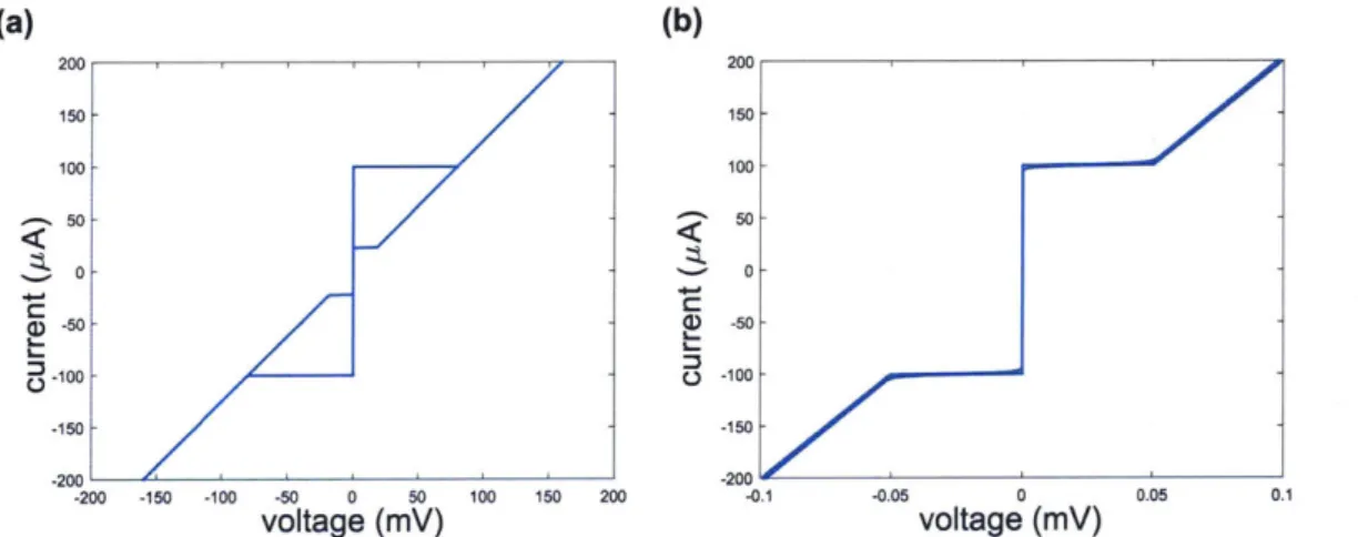
voltage characteristics of the devices. Fig.2.3 shows the simulated
current-voltage relation for an unshunted and a shunted superconducting nanowire.
(a) (b) 200 200 150 150 100 100 -~50 - 50 0 S0 -50 ID -50 1.200 -100 -150 -150 / 0 r -2001 -200 -200 -150 -10 -50 0 50 100 150 200 -0.1 -0.05 0 0.05 0.1 voltage (mV) voltage (mV)
Figure 2-3: Simulated IV characteristics of (a) shunted and (b) unshunted
supercon-ducting nanowires.
It can be seen that the unshunted nanowire shows hysteretic switching
character-istics (Fig.2.3a) while the shunted nanowire does not (Fig.2.3b). Circuits involving
superconducting nanowires will be shown in more detail in Chapters 3 and 4. On
the other hand, the work conducted in this thesis does not involve fabrication or
experimental characterization of JJs. However, it certainly is a main feature of the
simulator built in this work, to be able to simulate JJ based circuits. For these rea-sons, here we show the simulated responses of the Josephson junction and SFQ logic circuits. Fig.2-4 shows the experimentally characterized and the simulated IV curve of a shunted Josephson junction.
200 150 100 50 0 U -50 -100-.2 -200 -100 0 100 200 300 Voltage (p V)
Figure 2-4: Experimental result for a shunted Josephson junction (back) taken from Ref. [46] and simulation result generated by the simulator constructed in this work (front). Switching current of the simulated JJ is directly taken from Ref.[46j, while the other circuit parameters (that effectively define the Stewart-McCumber parameter) are modified manually to obtain the same characteristics, as they were not reported in the original experimental data.
It can be seen that the switching characteristics of the device are non-hysteretic as the junction we use here is resistively shunted. As it is a simulation involving a Josephson junction (the characteristics we show here in Fig.2-4 is essentially DC Josephson effect), we have used the phase-coherent solver.
Following this validation, we have also examined the area of the voltage pulse, generated by this junction. This value was obtained by integrating the output voltage of a Josephson transmission line (JTL) over time. Simulated response provided this number to be 2.0678 fV s, which is within 0.03 aV s of the expected value of the flux quantum (<bo = )
Following the validation of the single device characteristics with our simulator, we have proceeded to test the behavioral level simulations, using well-known SFQ logic circuits. All of the logic gates (AND, OR, buffer, NOT, NOR, XOR etc.), and
fundamental elements (SQUIDs, JTLs etc.) we have tested have produced expected
results, compatible with experimentally characterized responses. Here we show only a
few of those examples. Fig.2-5 shows the simulated response of the SFQ logic NAND
gate, which has the circuit schematic given in Fig.2-2. In the simulation panes, dashed
red-lines indicate the clock timings, while the blue lines indicate the timings of the
input pulses.
CLK
SInput Phase 6 Input Voltage 6
> 4-s
'.6 4* E 0. 0 0 20 40 60 s0 100 time (ps) Output Phase -2 0 40 60 so time (ps) Output Voltage0
. > 0. > 00 100 -2 time (ps) 0 20 40 60 80 100 time (ps)Figure 2-5: Operation of the SFQ logic based NAND gate shown in Fig.2-2. Phase
(left) and voltage (right) informations are shown throughout the operation where the
binary values of the signals noted on the graphs. It can be seen that output follows
the input after a one clock cycle delay.
It can be observed that the SFQ logic NAND gate has one clock cycle delay
between its input and output. Similarly, the circuit schematic of an SFQ logic AND
gate is given in Fig.2-6. Fig.2-7 shows the input and output voltages, where the gate
again shows a one-clock-cycle delay between its input and output.
As a final SFQ logic demonstration, we show a 3-bit counter, which consists of
many different SFQ logic elements. This circuit features 428 current sources (for
biasing the junctions), 553 JJs, and 458 inductors, creating 549 nodes, leading to a
1098 x 1098 system matrix.
TT IbAL T A LA JR J1 I 2A J A IbC CT A C B J SB JB C
Figure 2-6: Circuit schematic of an SFQ logic AND gate. Figure taken from Ref.
[22].
>6 2 0Input Voltage
0 20 40 60 80 10 time (ps)Output Voltage
E02 0 20 40 60 time (ps) 0 0 100Figure 2-7: Simualted responce
be seen that the output follows
of the SFQ logic AND gate shown in Fig.2-6. It can
the input after one full clock cycle delay.
We have observed that for the solution memory scales with O(N), and the peak
memory with O(N
2), where N is the number of nodes in the problem. On the other
had the computation time tends to scale with O(N-
5). The data points that have
led to these conclusions can be found in Table 2.1.
Parameter
NAND
3-bit Counter
Number of Nodes 35
549
Performance
101 ps/s
1.49 ps/s
Memory
4.03 kB/s 63.2 kB/s
Table 2.1: Performance metrics of the simulator, derived from SFQ logic device
sim-ulations.
V V t
I I I
I I
> 4 E > 4 E 2 0 75 0 > A
Output Low Bit
I
-0 50 100 150 200 250 300
time (ps) Output High Bit
rI
I I ' 1 90 50 100 150 200 250 300
time (ps)
Output Overflow Bit
I II
60
> 0 50 100 150 200 250 300
time (ps)
Figure 2-8: Simulated response of a 3-bit SFQ logic
counter.
After 100 ps, SFQ pulse
readings in respective ports read [0001, [001], [010], [011] and [110].
Typically, for circuits that operate at very low power and very high speed (such
as SFQ logic), operation margins are very tight. Therefore, the ability to perform
sensitivity analysis assists the designer greatly in realizing robust circuits. In Chapters
3 and 4 we will show how to use the simulator is utilized inside an optimizer to do
so. We will also realize those devices and demonstrate the capability of the software
in developing fast, scalable and power-efficient cryogenic computing elements.
Next step with this framework should be the expansion of the simulation
capa-bilities into the layout and logic levels. Our experience has shown that many design
malfunctions arise due to the underestimated parasitics, even more importantly, due
to inadvertent current crowding. A layout-versus-schematic (LVS) checker would be
highly beneficial to prevent such issues. Furthermore, to enable larger scale
imple-mentations a hardware description language (HDL) implementation will be required
as well. Finally, effective transmission line models to better understand interconnect
effects and pulse timing properties would be essential in realizing such systems.
-F
I I j
I
I I I

![Figure 2-8: Simulated response of a 3-bit SFQ logic counter. After 100 ps, SFQ pulse readings in respective ports read [0001, [001], [010], [011] and [110].](https://thumb-eu.123doks.com/thumbv2/123doknet/14464965.521154/38.917.229.663.155.481/figure-simulated-response-logic-counter-pulse-readings-respective.webp)