HAL Id: hal-00808454
https://hal.sorbonne-universite.fr/hal-00808454
Submitted on 15 Jul 2019HAL is a multi-disciplinary open access
archive for the deposit and dissemination of sci-entific research documents, whether they are pub-lished or not. The documents may come from teaching and research institutions in France or abroad, or from public or private research centers.
L’archive ouverte pluridisciplinaire HAL, est destinée au dépôt et à la diffusion de documents scientifiques de niveau recherche, publiés ou non, émanant des établissements d’enseignement et de recherche français ou étrangers, des laboratoires publics ou privés.
Electrochemical behaviour of (111) B-Doped
Polycrystalline Diamond: Morphology/surface
conductivity/activity assessed by EIS and CS-AFM
Claude Deslouis, Jacques Sanoit (de), S. Saada, C. Mer, Alain Pailleret,
Hubert Cachet, P. Bergonzo
To cite this version:
Claude Deslouis, Jacques Sanoit (de), S. Saada, C. Mer, Alain Pailleret, et al.. Electrochemical behaviour of (111) B-Doped Polycrystalline Diamond: Morphology/surface conductivity/activity assessed by EIS and CS-AFM. Diamond and Related Materials, Elsevier, 2011, 20 (1), pp.1-10. �10.1016/j.diamond.2010.10.005�. �hal-00808454�
Electrochemical behaviour of (111) B-Doped
Polycrystalline Diamond:
Morphology/surface conductivity/activity
assessed by EIS and CS-AFM
C.Deslouis ab, J.de Sanoit c, S.Saada c, C.Mer c, A.Pailleret ab, H.Cachet ab, P.Bergonzo c
(a) CNRS, UPR 15, Laboratoire Interfaces et Systèmes Electrochimiques, F-75005, Paris, France (b) UPMC, Univ. Paris 06, UPR 15, Laboratoire Interfaces et Systèmes Electrochimiques, F-75005, Paris, France
(c) CEA, LIST, Diamond Sensors Laboratory, F-91191 Gif-sur-Yvette, France
Abstract
Electrochemical activity, morphology and surface electrical conductivity of Boron-Doped Polycrystalline Diamond films prepared by MPCVD have been investigated. Heterogeneous apparent rate constants of three different redox systems, [Fe(CN)6]3−/4−, [IrCl6]2−/3− and [Ru(NH3)6]3+/2+ have been
measured by both Cyclic Voltammetry and Electrochemical Impedance Spectroscopy on < 100 > textured films with a predominance of (111) faces: first measurements have been done with [Fe(CN)6]3−/4− only on as grown samples, and secondly after a mild electrochemical pretreatment the
three redox systems have been investigated. “As-grown” samples showed a moderate average activity which was related to the presence of a minority of electronically conducting areas among insulating zones. Electrochemical treatment in neutral conditions substantially increased the activity and heterogeneous apparent rate constants kapp for the three couples were measured in the range of
10− 2 cm s− 1 with a good stability in time. Current-sensing AFM images performed ex situ showed that
the electrochemically pre-treated material presented a high superficial conductivity whereas the grown sample showed major area of low conductivity.
Keywords
Boron-doped diamond electrode, EIS, CS-AFM, Activity
1. Introduction
Boron-Doped Polycrystalline Diamond (B-PCD) thin films prepared by Chemical Vapor Deposition assisted by Microwave Plasma (MPCVD) are very promising materials for several applications in Electrochemistry [1], [2], [3] in particular in Analytical Electrochemistry and water treatment due to their wide potential window, their absence of parasitic current and their chemical stability. The origin of their electrochemical activity and its spatial distribution, the role of chemical surface terminations are always open questions. The latter is strongly connected to the nature and protocol of the applied surface treatment prior to electrochemical experiments. These treatments can be either physical by tailoring the deposition parameters in the reactor at the end of the process, or they can be electrochemical by imposing cathodic or anodic prepolarization conditions following prescribed procedures.
It is rather widely accepted that H-terminated Boron Doped Diamond (BDD) materials are more electrochemically active towards inner sphere reactions than O-terminated ones due to their negative electronic affinity, while outer sphere reactions would be insensitive to the termination. However, several factors may affect this activity: mode of synthesis, pre-treatment, dopant content, crystallinity.
For example, different values of the apparent rate constant for the ferri/ferrocyanide system ([Fe(CN)6]3−/4−) have been measured on BDD (2 × 10− 4 ≤ kapp ≤ 10− 1 cm s− 1) depending on the boron
content [4], [5], [6], [7], [8]. Significant kapp values (10− 2 cm s− 1 < kapp < 10− 1 cm s− 1) for the same
redox systems as those studied in this work have been also found for Nitrogen-containing Diamond films [9]; similarly, for films of amorphous carbon nitride materials like a-CNxHy or a-CNx, values in
the same range have been obtained: lower values (kapp ∼ 10− 4 cm s− 1) for the former [10] and higher
ones for the latter [11] (a few 10− 2 cm s− 1) consistent with the low potential difference found between
the oxidation and reduction peaks. These rate constant values strongly depend on the surface state of the materials, for example by varying the sp3/sp2 ratio [8], [12] by depositing graphite particles on BDD
substrate or by performing pre-treatments, either electrochemical or by plasma [13], [14], [15], [16], [17].
Several investigations tried to correlate the electrochemical activity with the chemical, electrochemical or plasma-assisted pre-treatments of the material surface and the nature of the terminations, ═O or ―H, was invoked to explain the observed effects. For example, Latto et al. [13] showed that for the ferrous– ferric couple, an oxidizing pre-treatment on BDD films enhances the electron transfer rate. Ferro and De Battisti [14] showed a decrease of activity with respect to ferri-ferrocyanide couple for oxidized films. In most cases, cathodic pre-treatments resulted in improved electron transfer [15], [16], [17]. Anodic pre-treatment is likely to form carbonyl or carboxyl groups which are nucleophilic and therefore slow down the electron transfer for redox reactions involving ligands as for ferri-ferrocyanide. Conversely, electrophilic terminations resulting from a cathodic pre-treatment favor electron transfer. However, if it is clear that hydrogen-terminated diamond films present extremely fast apparent transfer rates, it has been shown for B-PCD that both the air aging and the electrode use result in a monotonic degradation of the electrochemical performance, while by contrast, redox treated samples do not only recover their high activity and reversibility but also remain stable under an extensive electrochemical use even after weeks of exposure to air [18].
Most of the available data only yield an average activity and do not assess its local distribution. The Scanning ElectroChemical Microscopy (SECM) allows in principle to provide this information but the finest scale which is accessible by this technique is in the order of the tip size: the smallest tip diameter used in [19] for example was 2 µm and was consistent with the crystal size. It was shown that for moderate doping levels in boron, the activity seemed to be localized at grain boundaries. Macpherson and coworkers [20], [21] combined electrochemical method (CV) with SECM, AFM and C-AFM scanning probe techniques for characterizing the local activity of O-terminated acidic treated polycrystalline BDD. They could show that different conductivities (by C-AFM) are related to different levels of boron uptake in specific grains detected by the apparent rate constant kapp value (measured by
SECM in the generation mode). At variance with the results in ref. [19], they did not observe enhanced conductivity at grain boundaries. For finer grain sizes such as those used in this work, this approach is not appropriate in addition to the fact that the roughness is large and could corrupt the response. Another approach for mapping the local activity was proposed by Swain et al. [22] by using a chemiluminescent reaction sensing the local production of oxygen. It was shown that an as-grown BDD electrode is not uniformly reactive as the light emission was only detected on localized spots of the electrode area. Similarly, Becker and Jüttner [7] analyzed EIS data showing an impedance response in the mid frequency domain neither assigned to the electron transfer nor to the diffusion occurring on a uniformly reactive area. Conversely, they analyzed their data by assuming that electron transfer was occurring only at specific spots, which were assumed to be the grain boundaries. When the stationary individual diffusion layers do not coalesce, it is known that an additional diffusional response corresponding to the individual response of the active sites is observed. This behavior [7] was only observed for samples having moderate doping levels. Mahé et al. [8] also identified those active spots as Csp2 microdomains
Another factor involved in the electrochemical activity which was already viewed is the crystal orientation. According to several authors, (111) faces show higher apparent rate constants and possibly narrower potential window [23], [24]. This is presumably explained by the higher boron content on those faces.
In this work, activity of < 100 > textured B-PCD samples with a predominance of (111) faces was assessed. This activity was analyzed by using three redox systems, ferri/ferrocyanide, Hexachloro-Iridate IV/III, Hexaammino-Ruthenium II/III couples, and by means of Electrochemical Impedance Spectroscopy (EIS). The first redox couple is the most often used though it does not possess an outer sphere character in particular because it is sensitive to the properties of the substrate surface. The other two ones are outer sphere redox systems and tested for comparison. A thorough analysis of electrochemical performances of BDD thin films of different origins has been conducted with these three redox systems in [25]. Hydrogen-terminated surfaces provide apparent heterogeneous electron transfer rate constant kapp between a few 10− 2 to 10− 1 cm s− 1 ranges for the three systems.
So as to provide additional information on the local activity, Current-Sensing mode of AFM (CS-AFM) was used (the technique is the same as the C-AFM used in refs. [20], [21]). The principle consists in imposing, in ex situ conditions, a potential bias between the sample and the AFM tip coated by a thin conducting film. The local current is measured while the AFM is operated in contact mode which provides both the morphology and the local superficial electronic conductivity of the material at the nanometer scale. This is a prerequisite condition–but not a proof–for the local electrochemical activity, but obviously the material needs actually to be electronically conducting for electrochemical experiments. These data have been completed with SEM-FEG observations as a comparison with the morphological information provided by AFM.
2. Experimental
2.1. Preparation and characterization of the B-PCD films
A conductive polycrystalline diamond film with a {111} {100} < 100 > texture has been synthesized in three steps by MPCVD on p-Si (111) substrates (300 µm thick):
(1) Bias Enhanced Nucleation in situ pretreatment was used for the nucleation step (bias voltage of − 307 V, microwave power of 600 W, pressure of 30 hPa, 10 % CH4in 90% H2, temperature of 1023 K
and total flow of 120 sccm (standard cubic centimeter per minute), duration of 6 min, to achieve high nucleation density (> 1010 cm− 2).
(2) This nucleation step was followed by a selective growth step to develop (111) faces for 17 h (average thickness of 850 nm) with the following process parameters: microwave power of 600 W, pressure of 20 hPa, 0,6 % CH4 in 99,4 % H2 with 25 ppm of N2, total flow of 180 sccm and temperature of 953 K.
(3) The sample was further introduced in a boron doping reactor for the growth of an ultra thin (37 nm) homoepitaxial conductive layer of BDD (1020 cm− 3 < [B] < 1021 cm− 3). Trimethylboron was used as the
boron source at a flow rate of 10 sccm (2000 ppm), microwave power 1500 W, pressure 60 hPa, temperature 1000 K, CH4 0.8% in 99.2 % H2, total flow rate of 100 sccm during 4 h. The final stage
consisted in submitting the sample to a plasma under hydrogen flux at 1120 K (500 sscm, 100 mbars) during 20 mn. After the plasma had been turned off, samples were cooled under the same hydrogen flux for 2 h down to ambient temperature. Hydrogen flux was cut after cooling to avoid (or minimize) diamond oxidation. After mounting, the diamond electrode has been first tested as grown, and then further activated by cycling (10 cycles) in an aqueous and desaerated (Ar) 0.5 mol L− 1 LiClO
4 solution
between − 1.7 and + 1.7 V vs. Ag/AgCl (3 mol L− 1 KCl solution), the procedure being completed at
zero overpotential after an anodic sweep, which corresponds to mild oxidative conditions able to change the nature of the surface bonds. The use of this salt, especially the perchlorate anion, ensures that oxygen evolution is not preceded by another oxidation coming from the anion, namely the chlorine evolution with KCl.
Let us mention that other pretreatments have been recommended, in particular by McCreery et al. [26] for glassy carbon and further extended to BDD, consisting in soaking electrodes for 20 mn in distilled isopropanol prior to electrochemical measurements.
2.2. CS-AFM and SEM-FEG observations
AFM and CS-AFM observations were carried out in air using a Molecular Imaging instrument in the contact mode (deflection and topography images). This latter was composed of a Pico-LE base equipped with a micro-positioning device aimed at the precise positioning of the AFM tip in the x–y plane of the sample, a large zone scanner (100 µm × 100 µm) bearing a photo detector and the AFM nose adequate for CS-AFM experiments. The current range of the CS-AFM nose was − 10 nA/+10 nA. A PicoScan 2100 controller connected to a computer was used to drive the scanner and to collect the data generated by the laser impact on the photo detector. In this purpose, conducting AFM probes made from rectangular silicon cantilevers bearing conical silicon tips coated with a Pt-Ir alloy thin film were used. The curvature radius at the apex was 35 nm in average and the spring constant was within the range 0.5– 9.5 N m− 1 with a typical value close to 5 N m− 1. The loading force on the cantilever was maintained to
zero value. This condition was chosen so as to spare the metallic coating of the tip as wear risks were observed to be very high on this family of materials. Three images were successively made at the same spot to ensure that neither the AFM tip nor the samples were damaged. With the help of this rather heavy procedure, it was concluded that topography and local current images were never altered by any kind of variations from a sample to another.
SEM-FEG observations have been conducted with an ULTRA 55 FESEM from CARL ZEISS SMT allowing nanometer scale resolution with a magnification up to 800,000.
The electrochemical set-up consisted of an electrochemical interface AUTOLAB PGSTAT 30 (from Eco Chemie) equipped with an impedance module for EIS measurements. Impedance data were obtained in potentiostatic conditions, the signal amplitude being of 20 mV peak-to-peak. The measurements have been carried out in a cylindrical cell (250 ml) with a classical three-electrode arrangement with (i) the working electrode, cut as rectangular sample (area ~ 0.6 cm2) and then glued with a conductive resin
containing silver particles on a flexible plastic strip wearing a thin copper film; as the silicon substrate was insulating, the electrical contact for electrochemical measurements was taken from above on the edges of the superficial conducting B-PCD layer; (ii) a counter-electrode made of a platinum wire mesh of large area, (iii) a Saturated Calomel Electrode (SCE) or Silver│Silver chloride (Ag/AgCl) as reference electrodes.
The experimental impedance diagrams were analyzed in the frame of the Randles equivalent circuit composed of a serial arrangement of the charge transfer resistance Rt, accounting for electron transfer, and a Warburg impedance for diffusion in the absence of convection. A constant phase element (CPE) instead of the double layer capacitance was put in parallel to account for the usually observed frequency dispersions: the corresponding impedance is defined as : ZCPE = 1/Q(jω)n, where ω/2π is the modulation
frequency (Hz) and Q is the CPE which identifies to a capacitance when the CPE exponent equals 1. All these elements were then fitted to the experimental impedance data with a simplex method. A constant relative uncertainty of 1% on the impedance modulus was imposed in the whole frequency range in the absence of an accurate knowledge of the error structure.
2.3. Solutions
Three different redox systems, [Fe(CN)6]3−/4−, [IrCl6]2−/3− and [Ru(NH3)]63+/2+ have been tested all at an
equimolar concentration of 10− 3 mol L− 1, with 0.5 mol L− 1 KCl solution as supporting electrolyte.
The potential window was assessed in desaerated (Ar) 0.5 mol L− 1 LiClO4 aqueous solutions for
3. Results and discussion
3.1. As grown films
As the history of the successive treatments is recognized as crucial for the film activity, the sequence of treatments is further detailed. In a first stage, the film as grown was dipped in a 0.5 mol L− 1 KCl solution
containing [Fe(CN)6]3−/4−. EIS experiments have been then carried out at the formal potential
(η = 0) E0 = + 0.21 V vs. Ag/AgCl of the system. The EIS diagrams plotted in the Nyquist plane show
the classical aspect for a redox system (Fig. 1): a semi-circle corresponding to the charge transfer process (charge transfer resistance in parallel to the double layer capacitance) and a straight line at 45° with respect to the axes characteristic of semi-infinite linear diffusion described as the Warburg impedance. However, a slight flattening of the semi-circle is observed which accounts for a frequency dispersion ascribable to a Constant Phase Element (CPE see above) [27], which is considered in place of the double layer capacitance of the Randles equivalent circuit. However, the charge transfer resistance
Rt (Ω) can be adequately fitted at the formal potential and kapp (m s− 1) is determined as:
(1)
=( )
R is the molar gas constant (8.314 J mol− 1 K− 1), T the temperature (K), F the Faraday constant (96485 C
mol− 1), A the geometrical electrode area (6.4 × 10− 5 m2) and c∞ the redox species concentration (1 mol
m− 3).
Fig. 1. Impedance diagrams plotted in Nyquist coordinates for the [Fe(CN)6]3−/4− couple (10− 3 mol L− 1)
in 0.5 mol L− 1 KCl solution, at the formal potential (E0 = + 0.21 V /(Ag/AgCl)). Measurements
performed on as-grown B-PCD electrode (area 6.4 × 10− 5 m2): (■) 1st measurement (Rt = 416 Ω), (○)
2nd measurement (Rt = 483 Ω), (∆) 3rd measurement (Rt = 484 Ω). Electrolyte resistance Re = 58 Ω.
kapp value expressed in cm s− 1 for comparison with literature is around 10− 3 (see Table 1, “a” condition)
which lies in the mid range values reported earlier for moderately reactive electrodes especially without any pretreatment. Incidentally, between the first and subsequent other two diagrams kapp is shown to
slightly decrease within 15%. The sample is then submitted to cyclic voltammetry in the range (− 0.150, + 0.650 V/SCE). The voltammograms in Fig. 2 plotted for several scan rates show the aspect found for quasi reversible systems and have been therefore analyzed to determine the heterogeneous apparent rate
constant, following the procedure described by Nicholson [28]. As capacitance was not systematically investigated with potential and due to the lack of data on the structure of the double layer for such electrodes [29], the Frumkin correction was not carried out. The value in Table 1 (1.1 10− 3 cm s− 1)
indicates a stable activity after the first EIS experiments. A new sequence of EIS measurements at the formal redox potential is then performed. The EIS diagrams (not shown here) are similar to those in Fig. 1 but the size of the high frequency loop is increased by about 25 %, indicating a reduced activity. Therefore, an “as-grown sample” shows a decreasing activity with operating time under electron transfer as recently shown for the same type of material synthesized under the same conditions [18].
Table 1. Apparent rate constants for the [Fe(CN)6]3−/4−, [IrCl6]2−/3− and [Ru(NH3)6]3+/2+redox systems
measured by cyclic voltammetry (after ref. [28]) and by EIS (equation (1)). “a, b and c” conditions correspond to the sequence of measurements for the “as grown sample”: 1st EIS diagrams, 1st cyclic voltammetry, 2nd EIS diagrams.
[Fe(CN)6]3−/4− [Ru(NH3)6] 3+/2+ [IrCl6]2−/3− Before electrochemical
treatment electrochemical After treatment After electrochemical treatment After electrochemical treatment EIS Re (Ω) 58 ± 2 47 ± 2 52 ± 2 51 ± 2 Rt (Ω) (a) 416 ± 10 483 ± 10 30 ± 4 26 ± 4 21 ± 4 nCPE 0.87 0.89 0.43 0.47 0.45 Q (F sn− 1) 7.1 × 10− 6 6.1 10− 6 (4.55 ± 0.25) 10− 4 (8.00 ± 0.25) 10− 4 (7.40 ± 0.25) 10− 4 Ceq (F cm− 2) 3.4 × 10− 6 3.6 × 10− 6 1.61 × 10− 6 10.5 × 10− 6 4.7 × 10− 6 k0 (cm s− 1) (9.6 ± 0.5) 10− 4 (8.3 ± 0.5) 10− 4 (1.4 ± 0.2) 10− 2 (1.6 ± 0.2) 10− 2 (2.0 ± 0.3) 10− 2 CV k0 (cm s − 1) (1.1 ± 0.1) 10− 3 (1.5 ± 0.3) 10− 2 (1.5 ± 0.3) 10− 2 (1.3 ± 0.3) 10− 2
Prime novelty. This work shows clear evidence by CS-AFM of fully conductive BDD films after electrochemical pretreatments. This allows from EIS to give quantitative values to reaction rates of redox couples.
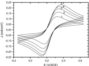
Fig. 2. Cyclic voltammograms performed after the impedance diagrams in Fig. 1. Same conditions as in Fig. 1. Scan rate: (1) 25 mV s− 1; (2) 50 mV s− 1; (3) 75 mV s− 1; (4) 100 mV s− 1; (5) 125 mV s− 1.
In diagrams of Fig. 1, it is also observed that the Warburg line displays a lower phase angle than 45°. As this occurs below a few Hz, the concentration modulated domain extends to a distance equivalent to (D/ω)1/2 ( about a few micrometers) from the electrode surface. This is much higher than the roughness
of the electrode, around 350 nm. In case of a totally active surface, one would normally find a true Warburg domain with a 45° phase angle as will be shown later. Therefore, without pretreatment, one may ascribe this CPE behaviour to non-homogeneous activity of the surface with active and inactive spots [7].
The observed CPE in the HF domain, can be analyzed according to Brugg et al. [27]and in general when the ohmic drop resistance, Re, and the charge transfer resistance, Rt, are comparable, an equivalent HF capacitance is proposed as:
(2)
= / + !( )/The calculated values (3.4 and 3.6 µF cm− 2 see Table 1) are expected for moderately doped BDD
electrodes and carbon materials in general [30].
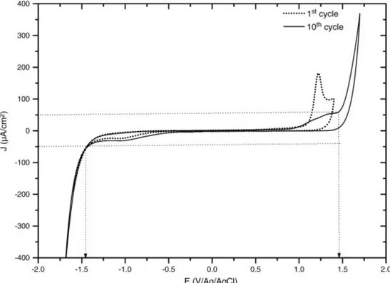
3.2. Activated films
After the second sequence of EIS measurements (see above), the same B-PCD film is electrochemically activated as detailed in Section 2.1. In Fig. 3 the voltammograms of the first and tenth cycles are displayed showing a 3 V potential window bounded by the current limits ± 50 µA cm− 2. However, small
anodic (+ 1.25 V vs. Ag/AgCl) and cathodic (− 0.6 V vs. Ag/AgCl) waves are observed before O2 and
H2 evolution reactions respectively. The small cathodic wave may be attributed to an incomplete
Fig. 3. Voltammograms (1st and 10th cycles in 0.5 mol L− 1 LiClO
4 solution) plotted during the
electrochemical activation conditioning of the B-PCD electrode after the measurements corresponding to Fig. 1, Fig. 2.
The B-PCD film is then submitted to cyclic voltammetry in presence of the three redox systems at different scan rates. The systems appear now as fast and reversible, which is confirmed by the potential difference between the peaks which is close to 60 mV (Fig. 4), and the proportionality of the cathodic and anodic peak currents to the square root of the scan rate ν (not shown).
Fig. 4. Cyclic voltammograms on the B-PCD electrode in 0.5 mol L− 1 KCl solution containing: (A)
[Fe(CN)6]3−/4− (10− 3 mol L− 1); (B) [IrCl6]2−/3− (10− 3 mol L− 1); (C) [Ru(NH3)6]3+/2+ (10− 3 mol L− 1); Scan
rates : (1) 25 mV s− 1; (2) 50 mV s− 1; (3) 75 mV s− 1; (4) 100 mV s− 1; (5) 125 mV s− 1; (6) 150 mV s− 1.
Impedance diagrams plotted at the formal potential confirm this result, as an example displayed by the ferri-ferrocyanide system in Fig. 5: the activation loop in the high frequency region is hardly visible and the Warburg region is well defined with only a negligible deviation with respect to the expected 45° phase angle with the axes in the mid and low frequency ranges.
Fig. 5. Impedance diagrams, on the B-PCD electrode, plotted in Nyquist coordinates in 0.5 mol L− 1 KCl
solution, recorded after potential pre-treatment for the [Fe(CN)6]3−/4−couple (10− 3 mol L− 1) at the rest
potential (E0 = + 0.21 V /(Ag/AgCl)). The High Frequency region is displayed in the inset. (□)
experimental data; (○) fitted data.
The same procedures as those used for the “as grown sample” for calculating the rate constant values were applied for both impedance and cyclic voltammograms.
Higher values of the heterogeneous apparent rate constant were found by cyclic voltammetry or by EIS for the three systems with only slight differences between them. kapp values in Table 1, around 10− 2 cm
s− 1, are in the range of the high reported ones in literature for B doping just below or at the SC-metallic
transition [1], [8], [22]. The accuracy afforded by the two techniques for the apparent rate constant assessment in that range is of course less but the agreement between the two sets of values is still quite satisfactory (see Table 1).
It is noteworthy to observe that the CPE exponent which was slightly lower than 0.9 before pretreatment has strongly decreased to values around 0.45 after pretreatment as reflected by the flatness of the HF region displayed in the inset of Fig. 5. This suggests that the role of diffusion is not correctly taken into account in the data analysis.
Actually, the smaller Rt values lead to a situation where the impedance corresponding to the reactive loop (Rt size) and the diffusion impedance are of the same order in the range of a few kHz, and not of a few Hz as before pretreatment. This frequency precisely corresponds to similar size scales for the electrode roughness (rms around 350 nm) and the extent of the modulated diffusion layer thickness ((D/ω)1/2 ~ 400 nm for 5 kHz assuming D = 8 × 10− 6 cm2 s− 1).
Thus, when frequency increases, the modulated diffusion layer becomes thinner as ω− 1/2 and therefore
follows more closely the actual roughness profile. The electrode area “seen” by the modulated diffusion layer increases thus from the projection (geometrical) area to the effective area above a cut-off frequency not determined here. In case of a pure fractal geometry, a CPE exponent has been predicted for a
diffusion process which is related to the dimension Df of the fractal geometry as ω(Df− 1)/2 [31], [32]. In
ref [33], such a correlation between fractal morphology characterized by AFM and cyclic voltammetry measurements was analyzed as due to the existence of non-contiguous reactive sites.
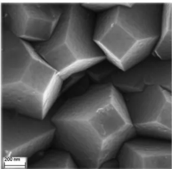
EIS measurements have been completed with SEM-FEG, AFM and CS-AFM imaging performed on samples after electrochemical activation: morphology images by SEM-FEG displayed in Fig. 6 are characteristic of the {111} {100} < 100 > texture showing truncated octahedrons defined by (111) faces with a square base. A larger scale analysis of the distribution between (100) and (111) faces, considering truncated octahedrons with lower and upper bases having 720 nm and 220 nm sides respectively, leads to 7% ± 2% for (100) and 92% ± 2% for (111) faces. The BDD film is therefore quasi (111) homoepitaxial.
Fig. 6. Field Emission Gun Scanning Electron Microscopy (Carl Zeiss Ultra 55) image (1.6 µm × 1.6 µm) of “as grown” B-PCD surface according to synthesis conditions defined in Section 2.1.
As (111) faces are known to accept a maximum boron doping level about ten times higher than the (100) faces, the average boron content in the sample should correspond to the semi conductor to metallic transition. Current–potential curves (not shown here) plotted at fixed points confirmed that the white areas are very conductive (saturation current at 10 nA is reached for very small bias potentials) while dark areas are insulating.
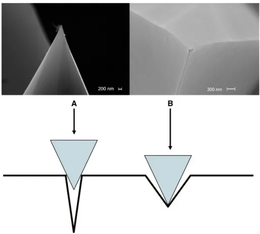
Morphology imaging by AFM in the contact mode at zero force (see topography (A) and deflection (B) images in Fig. 7) presents, with a close scale as in Fig. 6, a very similar aspect. The well defined geometrical features of the surface can be visualized on a profile scan along a horizontal line taken in Fig. 7. Such a profile (Fig. 8) shows segments of straight lines corresponding to the lateral and top faces of the octahedrons. One can then compare the steepest slopes in Fig. 8 (about 34° between 500 and 600 nm, and about 36° between 1500 and 1600 nm with respect to the vertical), which are also among the steepest ones for the whole image, to the half-angle of the circumscribed cone around the AFM tip. From SEM images shown in Fig. 9, this half-angle was estimated to be around 26° and therefore, situation “B” (Fig. 9) rather than “A” prevails, allowing one ensuring that most of the surface details were explored by the AFM tip.
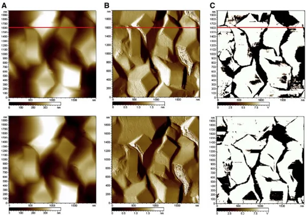
Fig. 7. Current-Sensing Atomic Force Microscopy imaging ( “A” topography images, “B” deflection images and “C” conductivity images, 2 µm × 2 µm) of B-PCD surface after electrochemical pre-treatment.
The three upper images and the three lower images represent two subsequent imaging (1st and 2nd sweeps respectively) of the same area for sake of reproducibility due to possible abrasion of the metallic coating (Pt-Ir) of the AFM tip. Potential bias applied to the substrate vs. tip: + 0.5 V. Red line shows the chosen scanned line for morphology and conductivity profiles in Fig. 8.
Fig. 8. Profile scanned on a line by the CS-AFM tip corresponding to the images in Fig. 7. Left axis, topography profile; right axis, local current measured between the substrate and the tip.
Fig. 9. Upper photographs of the CS-AFM tip taken with the FEG-SEM after imaging of Fig. 7. Cases A and B correspond to close or open valleys respectively for the AFM tip. AFM and CS-AFM imaging correspond to situation “B.”
As the tip apex contacted most of the sample, the conductivity image appearing in Fig. 7 (“C” images) reproduced fairly well the local conductivity with no or only slight geometrical convolution artifacts. In this image, bright zones represent highly conductive areas and it is visible in Fig. 8 (local current on right axis) that, on these areas, the current is saturated and so the local conductivity cannot be assessed considering the low potential bias (0.5 V) imposed between the tip and the substrate.
Even though local electrical conductivity (by CS-AFM) and local electrochemical activity (e.g. by SECM) cannot be closely related, at least the former one is required for ensuring the latter. Thus, these CS-AFM data prove that the B-PCD film after pretreatment is almost fully conductive and no specific activity distribution can be expected according to the different faces. In addition, a drop in conductivity is observed in recessed zones, however, percolation between grains is ensured since the surface appears as perfectly active.
So as to better estimate the effect of the final H2 plasma treatment at the end of the sample synthesis, the
same sample was submitted again to this process step (see above in Section 2.1). This procedure ensured thus that the boron content in the film was preserved. Fig. 10 displays two sets of mappings in the same sequence as in Fig. 7, i.e. from left to right: topography A, deflection B and conductivity C. These have been performed at quite distant locations from each other. They represent after several other scans quite extreme cases for conductivity that is expected to lie, as an average, in between. It appears that the conductivity (same 0.5 V bias as in Fig. 7) is much less than in Fig. 7 as dark zones occupy a larger area than the bright ones. When the two traces on a single scan for both the profile and the conductivity are plotted in the same figure (Fig. 11) one can see first that there is no transition between the high (saturated) and low (insulated) conductive domains and secondly that some faces are totally conductive and the others not.
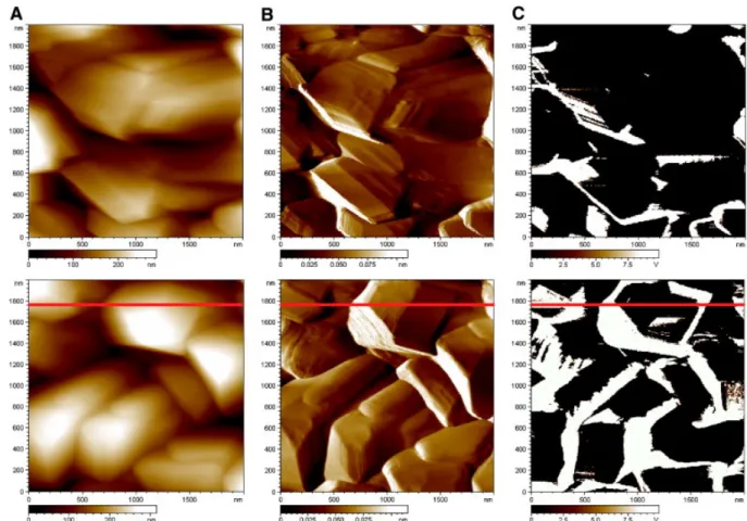
Fig. 10. Current-Sensing Atomic Force Microscopy imaging (“A” topography images, “B” deflection images and “C” conductivity images, 2 µm × 2 µm) of B-PCD surface after electrochemical pre-treatment and a new H2 cooling process restoring similar conditions of “as grown” sample. The three
upper images and the three lower images represent two subsequent imaging on different areas presenting various average electronic conductivity. Potential bias applied to the substrate vs. tip: + 0.5 V, same as in Fig. 7. Red line shows the chosen scanned line for morphology and conductivity profiles in Fig. 11.
Fig. 11. Profile scanned on a line by the CS-AFM tip corresponding to the images in Fig. 10. Left axis, topography profile; right axis, local current measured between the substrate and the tip.
In a recent similar study of poly(micro and nano)crystalline BDD films, Wang and Swain correlated topography and local electrical conductivity mapping by AFM and CP-AFM (a different denomination of the CS-AFM used here or the C-AFM used in refs [20], [21])[34]. Their analysis for CP-AFM images showed that the surface was shared between conductive and quite insulating areas as here but was only applied to as-grown samples for various B doping levels. For the highest ones, approaching (but below) the SC-metallic transition, wide conductive zones showed no preferential role of grain boundaries. They also concluded that B dopant could be heterogeneously distributed as it seems to be so here after H2 plasma cooling since some faces appear totally insulated (see the Fig. 11).
One has to explain the poor conductivity after the H2 plasma for the adopted synthesis conditions and
how it can be improved after the electrochemical pretreatment. First, it is known that the boron uptake represents the maximum value for the doping level in the BDD material: Interstitial H during synthesis and at the end of the process may actually form B–H pairing with substitutional B which gives rise to a passivation because boron atoms do not play their role as shallow acceptors and this corresponds to a lower doping level [35]. In anodic conditions, B–H complex can dissociate as:
B – H → B− + H+
B – H → B− + H° + h+
These two processes increase the free acceptor level and the concentration of holes as free carriers. This has been shown by Raman spectroscopy by the increase of the Fano resonance [36]. Then, oxidation of superficial H° could also explain the small anodic peak at about + 1.25 V (Fig. 3) which gradually disappears after the 10 imposed scans.
Another possibility concerning this small anodic peak can be found in the ref.[8] by Mahé et al. and is based on the role of residual graphite “fragments” issued at the end of the MPCVD elaboration. In fact, the first scan shows a rather narrow peak that was assigned in Ref. [8] to oxidation process in water on basal planes of graphite scales producing surface terminations of the carbonyl or hydroxyl groups. In that work, the authors purposely deposited graphite particles by HOPG abrasion on the BDD electrode. From the first scan, one can estimate a charge around 160 µC cm− 2, that corresponds to one monolayer
given a number of active sites of 1015 cm− 2. Concurrently, in the presence of basal graphite sites, the
rate constant value in [8]was found in the range 10− 3 cm s− 1. On the 10th and last scan, the anodic peak
is widened and lowered, possibly indicating a decrease of the graphitic sites. In a recent paper [37], similar anodic peak was found with cathodically pre-treated BDD electrode and was assigned to sp2 carbon.
5. Conclusions
In this work, B-PCD
thin films
with a predominance of (111) faces have been synthesized by MPCVD, and their morphological and surface electronicconductivity
, and electrochemical activity characterized by AFM and CS-AFM on the one hand, and by EIS andcyclic
voltammetry
on the other hand.The main results could be listed as follows:
Even after a controlled cooling under
hydrogen flux
in the MPCVD reactor, “as grown films” were found to be poorly reactive with respect to the [Fe(CN)6]3−/4−redox couple
.Potential scans in neutral medium, with mild successive
oxidation
and reduction conditions at the limits of hydrogen andoxygen evolution reactions
were able to activate the films up to highof the heterogeneous apparent rate constant kapp for the [Fe(CN)6]3−4−, [IrCl6]2−3− and
[Ru(NH3)]63+/2+ redox couples have been found and the film activity showed good stability in time.
CS-AFM proved that the local superficial BDD electronic conductivity was high and concerned most of the surface with, in particular, no conductivity increase in the grain boundaries. This allowed assigning a quantitative value to the measured rate constants by use of the effective electrode area determined by AFM imaging in the contact mode.
CS-AFM imaging of the surface after a subsequent hydrogen plasma similar to that applied after synthesis showed a significant decrease of the surface conductivity which was explained by a partial passivation of BDD film due to the formation of B–H pairs leading to a decrease of the acceptor levels in the film.
The explanation proposed for the improvement afforded by the mild anodic polarization pre-treatment pointed either to the dissociation of the B–H pairs with a concurrent increase of the acceptor level, thus increasing the material conductivity or to eliminating the residual graphite domains formed in the last stage of the synthesis process from the surface.
Acknowledgements
The authors acknowledge the contribution of Stephan Borensztajn who performed the SEM-FEG experiments at LISE laboratory and Emilie Vanhove (PhD Student at CEA) for valuable discussions during the course of this work.
References
[1] M.C. Granger, M. Witek, J. Xu, J. Wang, M. Hupert, A. Hanks, M.D. Koppang, J.E. Butler, G. Lucazeau, M. Mermoux, J.W. Strojek, G.M. Swain. Anal. Chem., 72 (2000), p. 3793
[2] Y. Show, M.A. Witek, P. Sonthalia, G.M. Swain. Chem. Mater., 15 (2003), p. 879
[3] M. Hupert, A. Muck, J. Wang, J. Stotter, Z. Cvackova, S. Haymond, Y. Show, G.M. Swain. Diamond Relat. Mater., 12 (2003), p. 1940
[4] R. Ramesham. Thin Solid Films, 339 (1999), p. 82
[5] M.C. Granger, G.M. Swain. J. Electrochem. Soc., 146 (1999), p. 4551
[6] C. Lévy-Clément, F. Zenia, N.A. Ndao, A. Deneuville. New Diamond Front. Carbon Technol., 9 (1999), p. 189
[7] D. Becker, K. Jüttner. Electrochim. Acta, 49 (2003), p. 29
[8] E. Mahé, D. Devilliers, Ch. Comninellis. Electrochim. Acta, 50 (2005), p. 2263
[9] Q. Chen, D.M. Gruen, A.R. Krauss, T.D. Corrigan, M. Witek, G.M. Swain. J. Electrochem. Soc., 148 (2001), p. E44
[10] H. Cachet, C. Deslouis, M. Chouiki, B. Saidani, N.M.J. Conway, C. Godet. J. Electrochem. Soc., 149 (2002), p. E233
[11] A. Lagrini, C. Deslouis, H. Cachet, M. Benlahsen, S. Charvet. Electrochem. Comm., 6 (2004), p. 245
[12] I. Duo, A. Fujishima, Ch. Comninellis. Electrochem. Comm., 5 (2003), p. 695 [13] M.N. Latto, D. Jason Riley, P.W. May. Diamond Relat. Mater., 9 (2000), p. 1181 [14] S. Ferro, A. De Battisti. Electrochim. Acta, 47 (2002), p. 1641
[15] T. Kondo, K. Honda, D.A. Tryk, A. Fujishima. Electrochim. Acta, 48 (2003), p. 2739
[17] H.B. Suffredini, V.A. Pedrosa, L. Codognoto, S.A.S. Machado, R.C. Rocha-Filho, L.A.Avaca. Electrochim. Acta, 49 (2004), p. 4021
[18] E. Vanhove, J. de Sanoit, J.C. Arnault, S. Saada, C. Mer, P. Mailley, P. Bergonzo, M.Nesladek. Phys Stat. Sol., 204 (2007), p. 2931
[19] K.B. Holt, A.J. Bard, Y. Show, G.M. Swain. J. Phys. Chem. B, 108 (2004), p. 15117
[20] N.R. Wilson, S.L. Clewes, M.E. Newton, P.R. Unwin, J.V. Macpherson. J. Phys. Chem. B, 110 (2006), p. 5639
[21] A.L. Colley, C.G. Williams, U.D'.H. Johansson, M.E. Newton, P.R. Unwin, N.R. Wilson, J.V. Macpherson. Ann. Chem., 78 (2006), p. 2539
[22] J. Wang, M. Mermoux, G.M. Swain, G. Lucazeau, J. Zak, J.W. Strojek. New Diamond Front. Carbon Technol., 9 (1999), p. 317
[23] Yu.V. Pleskov, Yu.E. Evstefeeva, V.P. Varnin, I.G. Teremetskaya. Russ. J. Electrochem., 40 (2004), p. 886
[24] T. Kondo, Y. Einaga, B.S. Sarada, T.N. Rao, D.A. Tryk, A. Fujishima. J. Electrochem. Soc., 149 (2002), p. E179
[25] A.E. Fischer, Y. Show, G.M. Swain. Anal. Chem., 76 (2004), p. 2553 [26] S. Ranganathan, T.-C. Kuo, R.L. McCreery. Anal. Chem., 71 (1999), p. 3574
[27] G.J. Brug, A.L.G. Van Den Eeden, M. Sluyters-Rehbach, J.H. Sluyters. J. Electroanal. Chem., 176 (1984), p. 275
[28] R.S. Nicholson. Anal. Chem., 37 (1965), p. 1351
[29] A.J. Bard, L.R. Faulkner. Electrochemical methods, Fundamentals and applications, Wiley, New York (2001)
[30] R.L. McCreery. Chem. Rev., 108 (2008), p. 2646
[31] P.G. de Gennes. Cr. Acad. Sci. Paris, 295 (1982), p. 1061 [32] L. Nyikos, T. Pajkossy. Electrochim. Acta, 31 (1986), p. 1347
[33] L.L.G. Silva, N.G. Ferreira, M.E.R. Dotto, M.U. Kleinke. Appl. Surf. Sci., 181 (2001), p. 327 [34] S. Wang, G.M. Swain. J. Phys. Chem. C, 111 (2007), p. 3986
[35] S.P. Mehandru, A.B. Anderson. J. Mater. Res., 9 (1994), p. 383
[36] P.C. Ricci, A. Anelda, C.M. Carbonaro, F. Clemente, R. Corpino. Thin Solid Films, 482 (2005), p. 311
![Fig. 1. Impedance diagrams plotted in Nyquist coordinates for the [Fe(CN) 6 ] 3−/4− couple (10 − 3 mol L − 1 ) in 0.5 mol L − 1 KCl solution, at the formal potential (E 0 = + 0.21 V /(Ag/AgCl))](https://thumb-eu.123doks.com/thumbv2/123doknet/12998162.379799/6.892.165.723.509.914/impedance-diagrams-plotted-nyquist-coordinates-couple-solution-potential.webp)
![Table 1. Apparent rate constants for the [Fe(CN) 6 ] 3−/4− , [IrCl 6 ] 2−/3− and [Ru(NH 3 ) 6 ] 3+/2+ redox systems measured by cyclic voltammetry (after ref](https://thumb-eu.123doks.com/thumbv2/123doknet/12998162.379799/7.892.114.841.370.887/table-apparent-constants-ircl-systems-measured-cyclic-voltammetry.webp)
![Fig. 4. Cyclic voltammograms on the B-PCD electrode in 0.5 mol L − 1 KCl solution containing: (A) [Fe(CN) 6 ] 3−/4− (10 − 3 mol L − 1 ); (B) [IrCl 6 ] 2−/3− (10 − 3 mol L − 1 ); (C) [Ru(NH 3 ) 6 ] 3+/2+ (10 − 3 mol L − 1 ); Scan rates : (1) 25 mV](https://thumb-eu.123doks.com/thumbv2/123doknet/12998162.379799/10.892.266.619.102.930/cyclic-voltammograms-electrode-solution-containing-ircl-scan-rates.webp)
![Fig. 5. Impedance diagrams, on the B-PCD electrode, plotted in Nyquist coordinates in 0.5 mol L − 1 KCl solution, recorded after potential pre-treatment for the [Fe(CN) 6 ] 3−/4− couple (10 − 3 mol L − 1 ) at the rest potential (E 0 = + 0.21 V /(A](https://thumb-eu.123doks.com/thumbv2/123doknet/12998162.379799/11.892.205.684.104.567/impedance-diagrams-electrode-nyquist-coordinates-potential-treatment-potential.webp)