HAL Id: tel-01578153
https://tel.archives-ouvertes.fr/tel-01578153
Submitted on 28 Aug 2017HAL is a multi-disciplinary open access archive for the deposit and dissemination of sci-entific research documents, whether they are pub-lished or not. The documents may come from teaching and research institutions in France or abroad, or from public or private research centers.
L’archive ouverte pluridisciplinaire HAL, est destinée au dépôt et à la diffusion de documents scientifiques de niveau recherche, publiés ou non, émanant des établissements d’enseignement et de recherche français ou étrangers, des laboratoires publics ou privés.
Study and modelling of the disturbances produced
within the STM32 microcontrollers under pulsed stresses
Yann Bacher
To cite this version:
Yann Bacher. Study and modelling of the disturbances produced within the STM32 microcontrollers under pulsed stresses. Other. Université Côte d’Azur, 2017. English. �NNT : 2017AZUR4021�. �tel-01578153�
Université Côte d’Azur – Polytech Nice-Sophia
École Doctorale des Sciences et Technologies de
l’Information et de la Communication
Electronique pour Objets Connectés – Polytech’Lab
Thèse de doctorat
Présentée en vue de l’obtention du
grade de docteur en Sciences spécialité Electronique
par
Yann BACHER
Etude et modélisation des perturbations
produites au sein des microcontrôleurs
STM32 soumis à des stress en impulsion
Thèse dirigée par Gilles JACQUEMOD Soutenance prévue le 27 Avril 2017
Jury :
Y. DEVAL Rapporteur Professeur, IPB Bordeaux
R. PERDRIAU Rapporteur Professeur associé, ESEO Angers
G. JACQUEMOD Directeur Professeur, UNS Sophia Antipolis
H. BRAQUET Co-Encadrant Professeur associé, Polytech Nice-Sophia
S. DELMAS BEN DHIA Examinateur Professeur, INSA Toulouse
- i -
Contents
List of figures ... iv
List of tables ... viii
Acronym list ...ix
Introduction ... 1
Chapter 1 Problematic introduction and state of the art... 3
1 Microcontroller ... 3
2 Microcontroller electrical stress test flow ... 5
2.1 Physical robustness tests and protections ... 6
2.1.1 HBM (Human Body Model) ... 6
2.1.1.1 HBM test description ... 6
2.1.1.2 ESD clamp protection ... 7
2.1.2 CDM (Chip Discharge Model) ... 7
2.1.2.1 CDM test description ... 8
2.1.2.2 CDM protections ... 8
2.1.3 Latchup ... 9
2.1.3.1 Latchup test description ... 10
2.1.3.2 Latchup protection ... 10
2.2 Electromagnetic compatibility (EMC) introduction standards and tests ... 11
2.2.1 EMC ... 11
2.2.2 EMC management impact on costs... 12
2.2.3 EMC coupling path and disturbances ... 13
2.2.3.1 Coupling paths ... 13
2.2.3.2 Disturbances ... 14
2.2.4 Standards ... 15
2.2.4.1 Standard creation flow... 15
2.2.4.2 Immunity standards ... 16
2.2.5 Susceptibility EMC tests applied on STM32 microcontrollers ... 17
2.2.6 Functional ESD test ... 17
2.2.6.1 Functional ESD protection ... 19
2.2.7 The Fast Transient Burst test ... 19
2.2.7.1 Test bench description ... 19
2.2.7.2 Test process ... 22
2.2.7.3 FTB protection ... 23
2.2.7.4 FTB analysis state of the art ... 23
3 Conclusion ... 26
Chapter 2 Stress propagation mechanism understanding ... 27
1 Supply pin number and placement consequence on FTB test results ... 27
1.1 Results ... 28
1.1.1 The impact of external regulator capacitor number ... 28
1.1.2 The impact of the number of supply couples ... 29
1.1.3 The impact of the supply placement ... 30
1.2 Conclusion about results ... 31
2 Common mode to Differential mode conversion hypothesis ... 32
- ii -
2.2 Common mode to differential mode conversion understanding ... 33
2.3 From concept to reality ... 36
3 Main parameters on common mode to differential mode conversion ... 36
3.1 Test bench parameters ... 37
3.2 Test board parameters ... 41
3.3 Package parameters ... 45
3.4 Chip parameters ... 48
3.5 Nonlinear effects due to protection diodes ... 50
3.6 Summary ... 51
4 Common mode to differential mode conversion versus frequency ... 53
5 Stress shape study ... 55
6 Conclusion ... 56
Chapter 3 Power network analysis methods ... 59
1 Power network behavior ... 59
1.1 Resonances and FTB disturbance ... 60
1.2 Pulse response measurement ... 62
1.3 RLC network resonance specificities ... 63
2 Resonance analysis methods ... 65
2.1 Global resonance analysis method ... 66
2.1.1 Measurement bench validation with simple circuits ... 67
2.1.1.1 A simple wire ... 67
2.1.1.2 Double wires ... 69
2.2 Microcontroller measurement ... 71
2.2.1 Differential mode resonance analysis ... 71
2.2.2 Common mode resonance analysis ... 72
2.3 Local resonances analysis methods ... 74
2.3.1 Local resonances ... 74
2.3.2 Local resonance measurement bench ... 75
2.3.2.1 Conducted emission measurement bench ... 75
2.3.2.2 Near field measurement bench ... 78
2.4 Investigation methods comparison ... 83
3 In silicon analysis ... 86
4 Conclusion ... 90
Chapter 4 Robustness improvement application & perspectives ... 93
1 Acting on external parameters modify robustness threshold ... 93
1.1 Which external parameters ... 94
1.1.1 Package ... 94
1.1.1.1 Supply and ground bonding diagram ... 94
1.1.1.2 Die pad connection ... 95
1.1.2 PCB supply tracks ... 95
2 Die pad effect study ... 96
2.1 Die pad contradictory influence ... 97
2.1.1 CHIP 1 ... 97
2.1.2 CHIP 2 ... 97
2.1.2.1 Die pad conclusion ... 98
2.2 How resonance tool helps to give coherence ... 98
2.2.1 CHIP 1 ... 98
2.2.2 CHIP 2 ... 99
2.3 Conclusion ... 100
- iii -
3.1 Resonance frequency shift using PCB and package on CHIP 2 ... 101
3.2 Resonance frequency shift of CHIP 1 by supply bonding diagram change 102 3.3 Conclusion ... 103
4 Perspectives ... 103
4.1 Using other tools ... 104
4.1.1 Debug flow and directives ... 104
4.2 How to shift resonance at wanted frequency ... 105
4.3 Modeling ... 105
General conclusion……….105
References………..109
Appendix A : Résumé en français………..113
- iv -
List of figures
Figure 1: Microcontroller schematic ... 3
Figure 2: ST microcontroller’s families [6] ... 4
Figure 3: Electrical stress test flow ... 5
Figure 4: HBM principle schematic and current waveform in a shorting wire . 6 Figure 5: ESD protection principle (positive stress) ... 7
Figure 6: CDM principle and current waveform for positive polarity ... 8
Figure 7: Output buffer schematic and silicon structure with parasitic bipolar transistors ... 9
Figure 8: Parasitic problematic bipolar structure ... 10
Figure 9: EMC issue gravity ... 11
Figure 10: EMC cost comparison ... 12
Figure 11: Disturbance propagation modes ... 13
Figure 12: EMC usual noise sources ... 14
Figure 13: Standards generating bodies ... 15
Figure 14: Functional ESD test bench ... 18
Figure 15: ESD generator principle schematic and stress shape in 50Ω load .. 18
Figure 16: Several cables in the same sheath ... 19
Figure 17: FTB test bench global schematic ... 20
Figure 18: QFP100 Test board ... 21
Figure 19: FTB test bench equivalent circuit schematic ... 21
Figure 20: Test process description ... 22
Figure 21: FTB stress shape ... 22
Figure 22: FTB generator equivalent circuit ... 23
Figure 23: EFT disturbs measurement ... 24
Figure 24: ICIM-CI schematic extracted from IEC 62433-4 standard [22] ... 25
Figure 25: The minimum and the maximum bonded supplies ... 28
Figure 26: Graphical representation of number of supply couples influence . 30 Figure 27: Supply placement influence ... 31
- v -
Figure 28: Common mode variation ... 32
Figure 29: Simple supply wires model ... 33
Figure 30: Common mode into differential mode conversion ... 34
Figure 31: Common mode to differential mode conversion QFP order of magnitude ... 35
Figure 32: Simplified multi supply wire bonding model ... 35
Figure 33: Influencing parameters studying parts ... 37
Figure 34: Test bench influencing parameters representation ... 38
Figure 35: Resistance formula ... 38
Figure 36: Inductance formula ... 39
Figure 37: Capacitance formula ... 39
Figure 38: Specific insulating plane schematic ... 40
Figure 39: Test board simplified supply equivalent schematic ... 41
Figure 40: SMD capacitor impedance versus frequency extracted from YAGEO Datasheet [27] ... 43
Figure 41: Board parameters schematic ... 44
Figure 42: Open QFP100 package ... 46
Figure 43: Generic QFP100 package resistance and self-inductance... 47
Figure 44: Package mutual inductance examples ... 47
Figure 45: Power distribution schematic ... 49
Figure 46: Protection diode on I/O ... 50
Figure 47: Main parameters summary ... 51
Figure 48: common mode to differential conversion global schematic ... 54
Figure 49: Common mode to differential mode conversion simulation of global schematic ... 54
Figure 50: Stress approximation ... 55
Figure 51: FTB measured versus theoretical spectrum ... 56
Figure 52: Two RLC circuit excited by an FTB stress simulation ... 60
Figure 53: Two ways providing frequency response of an invariant linear system62 Figure 54: Serial RLC ... 63
- vi -
Figure 55: Electric and Magnetic fields ... 64
Figure 56: 3 cascaded RLC circuits ... 64
Figure 57: Supply network electromagnetic field measurement principle ... 65
Figure 58: Resonance analysis measurement bench ... 66
Figure 59: Simple wire board setup ... 67
Figure 60: TEM Cell and GTEM Cell electrical spice simulation model ... 68
Figure 61: Simple wire resonance analysis simulation and measurement ... 69
Figure 62: Double wires board setup equivalent circuit ... 69
Figure 63: Double wires resonance analysis simulation and measurement .... 70
Figure 64: Microcontroller differential mode resonance analysis example ... 72
Figure 65: Common mode TEM Cell measurement ... 73
Figure 66: Common mode measurement setup result ... 73
Figure 67: Local resonance illustration ... 74
Figure 68: Conducted emission board ... 75
Figure 69: Conducted emission board high pass filter ... 76
Figure 70: IO buffer Vddio to output filter characteristic ... 76
Figure 71: Conducted emission measurement test setup ... 77
Figure 72: Local resonance measurement result example ... 77
Figure 73: Probe measurement path ... 79
Figure 74: Near field measurement bench ... 79
Figure 75: Langer Magnetic field probe [37] ... 80
Figure 76: Langer Electric field probe [39] ... 80
Figure 77: Magnetic field probe orientations ... 81
Figure 78: 3cm simple wire board schematic... 81
Figure 79: Simple wire near field measurement at its resonance frequency amplitude ... 82
Figure 80: Near field measurement result at 630 MHz ... 83
Figure 81: Internal measurement circuit principle ... 86
Figure 82: Diode regulator principle ... 87
Figure 83: ADC Flash and regulator schematic and simulation ... 87
- vii -
Figure 85: Level shifter based architecture schematic ... 88
Figure 86: Level shifter based architecture skew ... 89
Figure 87: Circuit layout alone... 89
Figure 88: Test chip layout ... 89
Figure 89: Test chip low frequency measurement (100 kHz) ... 90
Figure 90: Die pad in QFP100 package ... 95
Figure 91: STM32 F4 in all ST microcontroller families ... 96
Figure 92: CHIP 1 die pad influence on resonance ... 99
Figure 93: CHIP 2 die pad influence on resonance ... 100
Figure 94: CHIP 2 Resonance spectrum and FTB robustness threshold ... 101
Figure 95: CHIP 2 QFP144 and QFP100 Resonance spectrum t and FTB robustness threshold ... 102
- viii -
List of tables
Table 1: Test parameters ... 8
Table 2: Latchup test matrix ... 10
Table 3: IEC 61000-4-X standard ... 16
Table 4: Vcap influence on FTB test results ... 29
Table 5: Supply placement influence test results ... 30
Table 6: Insulating plane thickness comparison on a FTB test result ... 40
Table 7: Test bench RLC summary ... 41
Table 8: Board capacitance impedance order of magnitude ... 42
Table 9: Board RLC summary ... 44
Table 10: Microcontroller usual packages ... 45
Table 11: Package RLC summary ... 48
Table 12: Chip RLC summary ... 50
Table 13: Global RLC summary ... 52
Table 14: Parasitic elements sizes for simulation ... 53
Table 15: Stress response characteristics versus R L and C values ... 61
Table 16: CHIP 1 FTB results with and without die pad ... 97
Table 17: CHIP 2 FTB results with and without die pad ... 97
Table 18: CHIP 2 Resonance frequency shift and FTB robustness threshold summary ... 102
- ix -
Acronym list
AC: Alternating Current
ADC: Analog to Digital Converter CDM: Chip Discharge Model
CMOS: Complementary Metal Oxyde Semiconductor CPU: Central Processing Unit
DAC: Digital to Analog Converter DC: Direct Current
DIP: Dual Inline Package DUT: Device Under Test
EEPROM: Electrically-Erasable Programmable Read Only Memoy EFT: Electrical Fast Transient
EMC: ElectroMagnetic Compatibility EMC: electromagnetic compatibility EMS: ElectroMagnetic Susceptibility ESD: ElectroStatic Discharge
FTB : Fast Transient Burst
FTBth- : Fast Transient Burst negative robustness threshold
FTBth+ : Fast Transient Burst positive robustness threshold
GND: (GrouND) Used to describe the global perfect reference node GTEM Cell: Gigahertz Transverse ElectroMagnetic Cell
HBM: Human Body Model HF: High Frequency
IB: Immunity Behavior IC: Integrated Circuit
ICEM: Integrated Circuit Emission Model ICIM: Integrated Circuit Immunity Model IEC: International Electrotechnical Commission IO: Input/Output
- x - IP: Intelectual Properties
LF: Low Frequency
MCU: Microcontroller unit MCU: MicroController Unit PCB: Printed Circuit Board
PDN: Passive Distribution Network or Power Delivery Network QFP100: Quad Flat Package 100 pins
RAM: Random Access Memory
RLC: Used to describe circuit composed by resistor inductor and capacitor. ROM: Read Only Memory
SMA: SubMiniature version A (used for connectors) SMB: SubMiniature version B (used for connectors) SMD: Surface mounted device
SOC: System On Chip
SPICE: Simulation Program with Integrated Circuit Emphasis TEM Cell : Transverse ElectroMagnetic Cell
VDD: (Voltage Drain Drain) Used to describe the local power node VSS: (Voltage Source Source) Used to describe the local reference node
- 1 -
Introduction
This PhD work takes place in the Microcontroller Division of STMicroelectronics Company in partnership with EpOC laboratory, University of Nice Sophia Antipolis, and financed by the ANRT (Association Nationale Recherche Technologie). This work was done in the team responsible of IO development and Electromagnetic compatibility.
The robustness of products is a key to be distinguished in the competitive market of microcontrollers. A first thesis was made in the team regarding Electro Magnetic Interaction (EMI) by Jean Pierre LECA [1]. The aim of these researches was to create a reusable model to forecast EMI behavior of microcontrollers. Moreover this model permits also to find the weakness of a product and is proved to be very useful to improve performances. It is in the same context of continuous improvement, but this time on EMC susceptibility, that this new PhD work takes place.
Lot of work was done on Electro Static Discharge (ESD) to protect chips from physical damages [2]. It permits to create ESD protections and decrease losses during the manufacturing (Chip Discharge Model, CDM protections) and handling processes (Human Body Model, HBM protection). But ESD and more generally fast transient disturbance can occur during all the microcontroller’s life, and cause functional failures.
Studies on behavior of microcontrollers during fast transient are rare, whereas standard like functional ESD IEC 61000-4-2 [3] or FTB (Fast Transient Burst) standard IEC61000-4-4 [4] are references in EMC product evaluation. Physical ESD protections still work when the microcontroller is running and absorb a part of the stress but can’t prevent from disturbance on supply and signals.
Microcontrollers are composed by several sub-circuits which can be susceptible to disturbances. The environment (package, PCB) is also influent
2
- 2 -
parameters on robustness. Indeed it was observed that a sub-circuit integrated on different microcontrollers can be susceptible in one and not in the other. This work will focus on the study of the FTB test. Currently, concerning this test, the influence of such parameters are observed but not understood. Moreover, when a failure happens no measurement is possible to find the cause.
The aim of this thesis work is to understand the FTB stress propagation mechanisms and give tools to analyze failures and find ways to improve robustness. To achieve this, the manuscript is organized in 4 chapters.
The first one presents the context of this study and introduces the problematic. After a presentation of what is a microcontroller and its application field, an overview of the electrical test flow will leads to the presentation of the core of this work: the FTB test. To finish, measurement issues and the state of the art which are the reason of this work will be introduced.
The second chapter is dedicated to the FTB stress propagation mechanisms. Firstly the influence of the supply network will be studied. Results of this study will be used as a basis for the stress propagation understanding. It will lead to the formulation of a hypothesis which will be verified in the FTB test conditions.
In the chapter 3 power network analysis methods will be developed thanks to the understanding of the stress propagation. Based on resonance phenomenon, those tools will be presented and then compared to give a complete toolbox for chip analysis.
In the chapter 4 the contribution of this thesis work will be used with the objective of robustness improvement. The stress propagation understanding and tools will help to identify weakness of microcontrollers and keys to improve their robustness. To finish, perspectives opened by this work will be presented.
- 3 -
Chapter 1 Problematic introduction
and state of the art
1 Microcontroller
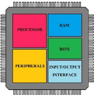
A microcontroller (MCU), depicted in Figure 1, is a complex System on Chip (SoC) which integrates on a single Integrated Circuit (IC), a processor core (Control Process Unit, CPU), memories (EEPROM, FLASH, and RAM), analog IPs and lot of Inputs/Outputs (IOs) [5]. The advantage of a microcontroller is that it reduces the size and the cost of a user application that uses microprocessor, memories and IOs separately. MCU are designed for embedded applications. Although they are designed in less aggressive technologies than microprocessors and working at lower frequencies.
Figure 1: Microcontroller schematic
The design of such system involves lot of core business. The main ones are Analogic, digital, IO and SOC design. Analog designers work mainly on peripherals (ADC, DAC, …) and supply regulation and monitoring. Digital designers work on processor, internal and external communication features. IO
Chapter 1 : Problematic introduction and state of the art
- 4 -
designers design the interface between the chip core and external pin including protection of the chip against external stresses. SOC designers are in charge of assembling all parts.
A microcontroller is a programmable chip and can be used in a wide application range. It is used for instance in washing machines, cell phones, medical, automotive, industry, robotic and so forth. To meet the market demand, several families of microcontrollers are developed. The Figure 2 shows STMicroelectronics microcontrollers’ families and their particularities. This study will focus mainly on STM32FX families which are made for mainstream and high performance applications. Those families contain 32 bit microcontrollers based on ARM Cortex cores. They are made with 180nm to 40nm technology nodes. Some products are still under development and many are already on the market.
Figure 2: ST microcontroller’s families [6]
To be a multi-application device implies to be compatible with all environment constraints. Humidity, temperature but also electromagnetic interferences are part of it. By this way, microcontrollers support several communication standards, a wide temperature range, and harsh electromagnetic environments. An electrical stress test flow is applied on products to evaluate their robustness performance.
Chapter 1 : Problematic introduction and state of the art
- 5 -
2
Microcontroller electrical stress test flow
To guarantee their robustness to electrical stress, microcontrollers are submitted to physical robustness test before functional EMC (ElectroMagnetic Compatibility) evaluation like illustrated in Figure 3. The Physical robustness test flow includes ESD like HBM (Human Body Model) [7], CDM (Chip Discharge Model) [8] and Latchup [9] tests. Those tests allow to know the limit beyond which the chip is subject to physical damages. If there is an abnormal robustness threshold at this step of the test flow, the microcontroller is modified for improvement by designers and has to be manufactured again.
Figure 3: Electrical stress test flow
EMC tests are performed while the microcontroller is executing a normal activity representative program. During tests, the correct behavior of the microcontroller is checked when it is submitted to different kind of stress. EMC tests take place after physical robustness evaluations so no physical damages are expected during this step. EMC tests are also made to verify that the chip does not disturb its environment. As well as the physical robustness tests, if an abnormal robustness or emission threshold is detected, the microcontroller returns to the design step for correction. The EMC topic is developed in the next part.
Chapter 1 : Problematic introduction and state of the art
- 6 -
2.1 Physical robustness tests and protections
2.1.1 HBM (Human Body Model)
During its movements, the human body accumulates charges by triboelectric effect [10]. By this way the body capacitance charges itself positively or negatively. When a person touches an object, his electrical potential can be different from the object and will be equilibrated by the capacitance discharge through the resistance of the body. The potential difference can reach several kV and the current several amps during a very short time.
2.1.1.1 HBM test description
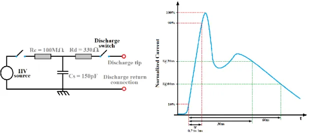
The HBM test is compliant with the ANSI/ESDA/JEDEC JS-001-2010 standard [7]. This test simulates the discharge of a human body in device pins to simulate an ESD during a handling. The ESD simulator reproduces the capacitance and the resistance of a human body with a 100pF capacitance which is discharged through a 1.5kΩ resistance. The schematic diagram of the ESD simulator is represented in Figure 4 with the current waveform in a shorting wire.
Figure 4: HBM schematic diagram and current waveform in a shorting wire
The current waveform depends on the load but the generator is calibrated by applying the discharge in a short circuit and normalized loads. During the test, a discharge is applied between each pin of the tested device. Each pin is tested with respect to all others for different voltage levels which
Chapter 1 : Problematic introduction and state of the art
- 7 -
reach several kV. If a physical damage is observed for a voltage below the maximum test limit, this voltage is considered as the robustness threshold. If no damage is observed until the maximum test voltage, the maximum voltage is written in the datasheet.
2.1.1.2 ESD clamp protection
When an ESD occurs, the capacitance is discharged from the higher potential to the lower through the chip. To protect circuits, the ESD current must flow from one pin to the other without damaging internal components. To avoid overvoltage and keep local voltage below the maximum supported by components, ESD clamp protections are implemented. Those protections have trigger voltage above maximum supply voltage but below circuit robustness limit. When this device is triggered, a low impedance path is created in parallel with the protected circuit and limits the peak voltage.
Figure 5: ESD protection principle (positive stress)
Diodes are placed on each pad which need to be protected and the ESD clamp system can be common to several or implemented in each IO, as shown in Figure 5. Diodes guide the current to the ESD Clamp protection. Notice that during handling the supply is not present.
2.1.2 CDM (Chip Discharge Model)
During manufacturing a chip is exposed to electrical fields and accumulates charges. Consequently when a pin is in contact with another electric potential a charge transfer happens. Discharge paths are different from HBM test. Other fails not covered by the previous test can be discovered and by this way, specific protections are also implemented.
Chapter 1 : Problematic introduction and state of the art
- 8 -
2.1.2.1 CDM test description
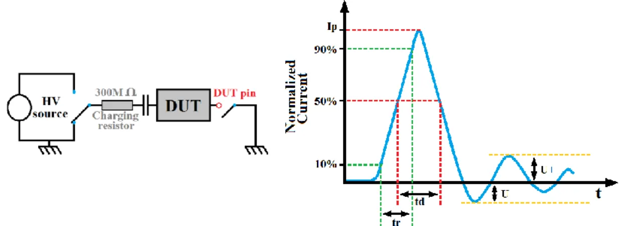
The JEDEC standard JESD22-C101E [8] describes the chip discharge model test which is applied on microcontrollers. This time, the chip is charged by an electric field positively or negatively and discharged in a ground plane. The Figure 6 represents the test bench principle and the stress current waveform in normalized condition extracted from the standard. The Table 1 synthetizes test parameters.
Figure 6: CDM principle and current waveform for positive polarity Table 1: Test parameters
Test Number
#1 #2 #3 #4
Standard test module Small Small Large Large Test Voltage (V) 500 (±5%) 1000 (±5%) 200 (±5%) 500 (±5%)
Peak current
Magnitude (A) Ip 5.75 (±15%) 11.5 (±15%) 4.5 (±15%) 11.5 (±15%)
Rise time (ps) Tr <400 <400 - -
Full width at half
height (ns) Td 1.0 (±0.5) 1.0 (±0.5) - - Undershoot (A,max) U- <50% Ip <50% Ip <50% Ip <50% Ip
Overshoot U+ <25% Ip <25% Ip <25% Ip <25% Ip
2.1.2.2 CDM protections
In the CDM case, the chip discharges itself through a pin. Whereas in the ESD HBM stress, two pins are involved, and the discharge current paths is managed thanks to the IO ESD network. During the ESD CDM stress, any internal wall (substrate p, isolated pwell, nwell) will accumulate loads and will have to find a discharge path to any contacted pin. As a consequence, the risk
Chapter 1 : Problematic introduction and state of the art
- 9 -
is located internally in the die, in a place where no ESD network is built. In this case, the main risk is that the best path for the current passes through transistor grid and breaks oxide or through any weak component. The principle of protection is to create preferential path for the current from internal accumulation area to pins.
2.1.3 Latchup
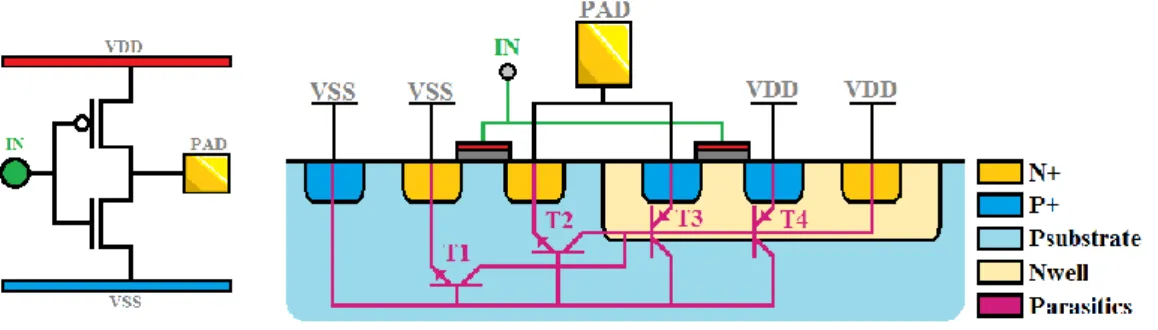
The latchup is a phenomenon due to parasitic NPNP structures in the silicon. Those structures can be triggered by over or under voltages on pins or supplies and create a very low impedance path between VDD and GND which can be hold. The latchup is responsible of functionality fails, over consumption or even physical damages on silicon. The latchup occurs mainly in IO if their design does not take into account the phenomenon, but can also occur in other areas as far as an external stress can reach them. A simple structure of an output buffer is depicted in Figure 7 to explain the phenomenon.
Figure 7: Output buffer schematic and silicon structure with parasitic bipolar transistors The cross section allows to visualize parasitic bipolar transistors which take part in the latchup phenomenon. An example of a problematic structure built with those transistors is represented in Figure 8.
Regarding the bipolar structure in Figure 8, if the PAD voltage increases over VDD about a diode threshold the transistor T3 turns on. The current from T3 flows in T1 and so T1 turns on and sinks current from transistor T4 which turns on also. The T4 and T1 structure is a low impedance path from VDD to VSS which is hold.
Chapter 1 : Problematic introduction and state of the art
- 10 -
Figure 8: Parasitic problematic bipolar structure
The same kind of phenomenon happens when the PAD goes under VSS with (T2, T4 and T1). More complex conditions can also cause latchup with other parasitic structures or dynamic effects.
2.1.3.1 Latchup test description
The latchup test permits to verify if most common latchup cases are present in the product. It consists in a current sink and injection on each pin and a verification of current consumption on the supply after. If there is no overconsumption on supply, the pin is considered as good. The Table 2 is the test matrix of the latchup test including overvoltage on supply.
Table 2: Latchup test matrix
PIN Logic state of all IO Test signal
IO low Current sink 100mA
IO low Current sink -100mA
IO high Current sink 100mA
IO high Current sink -100mA
Supply low Overvoltage test
Supply high Overvoltage test
2.1.3.2 Latchup protection
The first latchup protection is the layout implementation which takes into account parasitic structures. Decreasing bipolar transistor gain by taking collector away from emitter permits to decrease the loop gain of the NPNP structure. Lower the bulk resistance responsible from potential difference when current pass through it help to increase the trigger current. Adding guard ring degrades bipolar transistors gain and diverts current.
Chapter 1 : Problematic introduction and state of the art
- 11 -
2.2 Electromagnetic compatibility (EMC) introduction
standards and tests
2.2.1 EMC
The EMC definition is the following one:
“The ability of a device, equipment or system to function satisfactorily in its electromagnetic environment without introducing intolerable electromagnetic disturbance to anything in that environment” [11].
This is a wide definition of EMC, but there are important points to notice. The first one is that EMC concerns device immunity and emission. It means that a circuit can be a victim or an aggressor. The second point is the tolerance notion. Indeed the system has to function “satisfactorily” without introducing “intolerable” electromagnetic disturbances. The difference between a simple dysfunction or a critic dysfunction and a maximum level of emission has to be defined. This is standards job to determine limits. Of course the tolerance level depends also on the application. A dysfunction can be acceptable for a toy whereas it inadmissible for an airplane. Examples are given in Figure 9. Several standards exist depending on the domain (industrial, automotive, medical …).
Figure 9: EMC issue gravity
The earliest EMC issues go with first electricity applications in the middle of 18th century [12]. Since this period, EMC understanding hasn’t stop
Chapter 1 : Problematic introduction and state of the art
- 12 -
temperature or humidity. At the beginning EMC issues were solved case by case at the end of validation process, but research do not stop to improve models to solve EMC issues earlier in the product life.
2.2.2 EMC management impact on costs
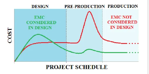
EMC has an impact on reliability of products but also on business and costs. Indeed tests and debug of EMC issues is time consuming and extends the time to market. An EMC issue not fixed in the production step impacts the reputation of the company in term of quality. The Figure 10 compares the EMC cost when considered during the design step and not considered at all. EMC consideration at the beginning increases the costs during the design step. But it lower the number of loop between designers and EMC validations and by this way the pre-production costs. The number of costumer supports decreases also during the production. The loss of customers, going to competitors because of EMC issue, is not represented in the graphic.
Figure 10: EMC cost comparison
Finding a way to quickly anticipate EMC issues is a serious stake technically and financially. Simulation at the design step would permit to reduce the time to market, customer issue risks and their impact in term of business. Considering EMC at the design step imply to have behavior models for emission and susceptibility.
Chapter 1 : Problematic introduction and state of the art
- 13 -
2.2.3 EMC coupling path and disturbances
2.2.3.1 Coupling paths
Disturbance are transmitted from a device to another by several ways. The Figure 11 illustrates usual coupling path between devices [13]. Notice that each device is a victim and an aggressor at the same time. In the Figure 11, a laptop and a smartphone both connected to supply and their unwanted interactions are represented.
Figure 11: Disturbance propagation modes
The laptop generates a noise which is transmitted to the smartphone by conduction in supply wires. The smartphone activity creates also a perturbation which affects the computer through supply wires. The same phenomenon happens through communication cables. Radiated disturbances are wanted in the smartphone case for communication purpose, but unwanted in the laptop case and due to the device activity, but in all case it induces noise in the environment. ESD has a specific propagation mode, it is conducted but come from external source like a charged human touching the device. It occurs when there is a contact or very close to contact between the source and the device.
Chapter 1 : Problematic introduction and state of the art
- 14 -
2.2.3.2 Disturbances
Unwanted signal can be called disturbance or noise. A noise can be generated by a device or from a natural source. Figure 12 represents a non-exhaustive list of noise sources [14] :
Natural noise sources o Magnetic storm o Thunderstorms o Atmospheric noise o Cosmic noise Industrial noise o Wireless communication o Motors o Lights Nuclear noise
Figure 12: EMC usual noise sources
Disturbance can be classified with their frequency spectrum, their propagation mode and duration. The noise is considered as Low frequency (LF) below 1MHz and High frequency (HF) above. A transient noise has a relatively short duration whereas a continuous noise is steady. This classification permits to have an idea of coupling phenomenon involved in the disturbance propagation.
Chapter 1 : Problematic introduction and state of the art
- 15 -
2.2.4 Standards
Compliance with EMC directives is done by self-certification to harmonized European or international standards. Manufacturer or importer can declare their product conform to a given set of standards, applies the CE mark and markets the product. It is up to the manufacturer to choose the appropriate standard to cover the maximum potential failure, and test it if necessary. The test process can also be done by an external subcontractor.
2.2.4.1 Standard creation flow
Standards propose a way to simulate immunity issues, measure emission of electronic systems, and give harmonized limits and levels. Standards are generated with the organization presented in Figure 13.
Figure 13: Standards generating bodies
IEC: International Electrotechnical Commission.
CISPR: French acronym for International Special Committee on Radio
Interference.
ACEC: Advisory Committee on EMC.
TC77: Is the Technical committee in charge of Electromagnetic compatibility. ETSI: European Telecommunication Standard Committee.
CENELEC: French acronym for European Committee for Electrotechnical
Standardization.
Chapter 1 : Problematic introduction and state of the art
- 16 -
TC77 and CISPR are two technical committees from IEC devoted to EMC work for other ones, EMC is only a part of their scope. The ACEC is responsible to prevent the development of conflicting standards in the heart of IEC. European standards are whenever possible based on IEC/CISPR results.
2.2.4.2 Immunity standards
This work is based on IEC immunity standards. Standard are classified with respect to the disturbance type. The IEC standard concerning EMC immunity tests is the IEC 61000 chapter 4 which is divided into several parts. A list of those parts with their description is presented in Table 3 extracted from the IEC website [15].
Table 3: IEC 61000-4-X standard
General
IEC 61000 - Electromagnetic compatibility (EMC) - Part 4-1: Testing and measurement
techniques - Overview of immunity tests (IEC 61000-4 series)
LF conducted disturbances
Part 4-11: Voltage dips, short interruptions and voltage variations immunity tests
Part 4-13: Harmonics and interharmonics including mains signalling at ac power port, low
frequency immunity tests
Part 4-14: Voltage fluctuation immunity test for equipment with input current not exceeding
16 A per phase
Part 4-16: Test for immunity to conducted, common mode disturbances in the frequency
range 0 Hz to 150 kHz
Part 4-17: Ripple on dc input power port immunity test
Part 4-27: Unbalance, immunity test for equipment with input current not exceeding 16 A per
phase
Part 4-28: Variation of power frequency, immunity test for equipment with input current not
exceeding 16 A per phase
Part 4-29: Voltage dips, short interruptions and voltage variations on dc input power port
immunity test
Part 4-30: Power quality measurement methods
Part 4-34: Voltage dips, short interruptions and voltage variations immunity tests for
equipment with mains current more than 16 A per phase
LF radiated disturbances
Chapter 1 : Problematic introduction and state of the art
- 17 -
HF conducted disturbances
Part 4-4: Electrical fast transient/burst immunity test Part 4-5: Surge immunity test
Part 4-6: Immunity to conducted disturbances, induced by radio-frequency fields
Electrostatic discharges
Part 4-2: Electrostatic discharge immunity test
Those standards are made for finished equipment. Microcontroller are not finished equipment but are designed to be a part of such device. EMC immunity and robustness levels are not the same for a microcontroller alone or embedded in a final application. For example, a chip susceptible to ESD stress can be completely safe in a final application if its pins are not accessible by the user. Or on the contrary, good electromagnetic emission with the chip alone can be amplified by the PCB routing of a final application. But in order to give information to customer and help them to make a choice between available products on the market, standards are also used and adapted to chips alones.
2.2.5 Susceptibility
EMC
tests
applied
on
STM32
microcontrollers
The EMC test flow of a microcontroller includes emission and susceptibility tests. For microcontrollers, two susceptibility tests are performed in our division: Functional ESD (IEC 61000-4-2) and Fast Transient Burst (FTB) (61000-4-4). Only FTB evaluation is studied in this work. However, these two kinds of tests are presented below.
2.2.6 Functional ESD test
The functional ESD test, specified in the 61000-4-2 [3], simulates a discharge when a program is running on the chip. The principle is almost the same as HBM test but the chip is supplied and capacitor and resistor values of the stress generator are not the same. The stress is applied on each pin of the device under test and its behavior is observed. The device has different kind of behaviors. It can function normally when a stress is applied, it can fail and reset,
Chapter 1 : Problematic introduction and state of the art
- 18 -
or it can fail and stay in indeterminate state. Each behavior has its level of gravity and can be acceptable or not depending on the application targeted.
A schematic of the test bench is depicted in Figure 14. This configuration is provided by the standard. Each element has its importance since it can impact the stress shape and thus the behavior of the tested device.
Figure 14: Functional ESD test bench
The test is performed for several voltage levels which go from 200V to 2kV on microcontrollers. The stress generator and stress shape in 50Ω load are described in Figure 15. The stress shape depends on load in which the discharge is applied. The standard describes a specific 50Ω load for the generator calibration.
Chapter 1 : Problematic introduction and state of the art
- 19 -
2.2.6.1 Functional ESD protection
Even if they are not designed specifically for this stress shape, ESD clamp protections have still an effect when the device is supplied and contribute to its protection. By this way devices are most of time not physically deteriorated. But some latchup effect can still be observed because new coupling paths appear which are not present in the latchup test since the stress shape is more aggressive.
2.2.7 The Fast Transient Burst test
The Fast Transient Burst (FTB) simulates a common mode conducted disturbance. This kind of perturbation happens when several devices have supply or signal wires in the same sheath (illustrated in Figure 16). In this case, if a motor starts, inrush current occurs in its supply cables and creates fast transient voltage variations. Due to capacitive coupling, a disturbance appears on other wires. This noise appears in all cables, this is a common mode perturbation.
Figure 16: Several cables in the same sheath
The FTB test was developed to take into account the maximum of switching transient cases even repetitive ones at a relatively high frequency (relay contact bounce). The principle of the test is to apply multiple fast transient burst in common mode by capacitive coupling. The FTB stress generator must guarantee specific rise and fall time, and sufficient amplitude. The device under test is supplied by a DC generator and is running. The robustness threshold of the device corresponds to the maximum stress voltage without fail.
2.2.7.1 Test bench description
This work, focuses on a specific FTB test, which is inspired from the IEC 61000-4-4 standard [4] but applied only on supply of microcontrollers. This
Chapter 1 : Problematic introduction and state of the art
- 20 -
standard is normally made for finished equipment, but is used here because there is no other standard which covers those potential fail cases. New standard [16] has been recently published to potentially cover those fail cases but not applied yet. The FTB test bench is presented in Figure 17.
Figure 17: FTB test bench global schematic
During the test, the device under test (DUT) welded on a test board is supplied by a DC Voltage source and the FTB stress is applied on the power supply through a capacitive coupler. The stress is provided by a FTB generator compliant with the standard. In this work, the Schaffner NSG 2025 will be used as a generator. An error return cable transmits the failure information to the FTB generator.
The Test board corresponds to IEC 61967-2 standard [17] with only 2 layers, a ground side and a power and signal side, as shown in Figure 18. Each supply is decoupled with 100nF capacitor as close as possible to the pin. The DUT is in its package and welded on the ground layer side of the test board.
Chapter 1 : Problematic introduction and state of the art
- 21 -
Power and signal layer Ground and chip layer
Figure 18: QFP100 Test board
A simplified electrical equivalent circuit is proposed in Figure 19. Inductors Lp protect the DC supply from the stress, Capacitors Cc represent the
capacitive coupler, and Cc2 is a capacitor which forces a common mode variation. Nets VDD* and VSS* correspond to the local supply after the capacitive coupler. At this point there is a common mode variation with respect to the ground.
Figure 19: FTB test bench equivalent circuit schematic
For this work the same generic test board will be used with several package footprints. It is also used for each EMC test flow (ESD, FTB, EMI …) and needs to be compatible with all those test benches. A QFP100 version of the board is represented in Figure 18.
Chapter 1 : Problematic introduction and state of the art
- 22 -
2.2.7.2 Test process
A specific test protocol, illustrated in Figure 20, was determined in order to minimize hazards [18]. The first step is done at positive low voltage level (200V), five tests are performed at each steps, the stress level increases until the DUT fails 5 times in a row or the maximum test limit is reached. Once the positive robustness level reached, the stress voltage level is decreased step by step in order to observe an eventual hysteresis phenomenon. The same process is done for negative stress voltages.
Figure 20: Test process description
The stress shape is described in Figure 21 which is extracted from the IEC standard. For each test the run duration is 12s. Bursts are applied on supply through the capacitive coupler with a repetition period of 300ms. Each 15ms long burst contains 75 pulses.
Chapter 1 : Problematic introduction and state of the art
- 23 -
The Figure 22 extracted from the standard IEC 61000-4-4 illustrates the stress generator principle. It must guarantee for a unique pulse 5ns rise time ±30% and 50ns fall time ±30%. The fall time is fixed by the size of the capacitor Cc and the resistor Rs. With the given schematic the management of the rise time
is left to the implementation of the generator made by the manufacturer of the device.
Figure 22: FTB generator equivalent circuit - Rc = charging resistor
- Cc = energy storage capacitor
- Rs = impulse duration shaping resistor
- Rm = impedance matching resistor
- Cd = DC blocking capacitor
2.2.7.3 FTB protection
There is no specific protection against FTB stress inside microcontrollers. The board implementation integrates decoupling capacitance and so on to decrease noise on supply but they are not placed for FTB purpose and there is no guarantee of their positive effect. The FTB stress mechanism is worth to be studied to find effective protections to improve microcontroller’s robustness.
2.2.7.4 FTB analysis state of the art
The FTB test is used to evaluate product robustness. However, the source of bad results at this test is hard to understand. In practice, when a device fails abnormally on a susceptibility test the root cause needs to be found for design correction. Usually, investigations start from the simple information of fail/pass to measurement and eventually simulations. Unfortunately during an
Chapter 1 : Problematic introduction and state of the art
- 24 -
Electrical Fast Transient (EFT) pulse as functional ESD or FTB stress, no measurement is possible due to electromagnetic disturbance (cf. Figure 23). Indeed, coupling on probe cable disturbs measurements when performed during the stress [19]. To provide some answers, the state of the art of the FTB analysis and investigation will be provided in this paragraph.
Figure 23: EFT disturbs measurement
Nowadays there is no efficient mean to investigate on FTB test fail other than empiric. Indeed when a fail is detected on a product, the impacted design is protected blindly expecting that the bug will be corrected. This method requires loops between design and validation which are time and cost consuming.
It was seen that no measurement are possible during the FTB stress. What about simulations? Because the stress is in common mode on supply, IBIS models (IO Buffer Information Specification) and IMIC (IO Model For integrated Circuits) are not adapted to the simulation of the stress. Few works deal with the EFT modeling in order to anticipate fails [20] using classic Passive Distribution Network (PDN) model or more complex ones [21].
The ICIM (Integrated Circuit Immunity Model) method is standardized in IEC 62433-4 standard [22] for susceptibility purpose. A principle schematic is depicted in Figure 24.
Chapter 1 : Problematic introduction and state of the art
- 25 -
Figure 24: ICIM-CI schematic extracted from IEC 62433-4 standard [22]
This model is composed by a Passive Distribution Network (PDN) and an active part modelled by an Immunity Behavior (IB). The Passive part represents the disturbance coupling path. The disturbance can be introduced through differential input terminals or single ended depending on the modelling level. The Immunity behavior part models the behavior of the device related to the level of disturbance applied. Based on immunity criteria it determines condition for which disturbance causes a fail. No electrical connection is made between the passive distribution network and the immunity behavior model.
The ICIM seems to be the most adapted to simulate circuit submitted to FTB stress. But this approach can’t be performed without knowing the injected stress. Indeed it will be seen later in this document that although the disturbance is about thousand volts, the resulting stress inside the die is suspected to be totally different. Without knowing this stress how is it possible to perform simulations?
Knowing stress mechanism is essential to perform efficient simulation and potentially use existing models. By this way it is possible in the end to
Chapter 1 : Problematic introduction and state of the art
- 26 -
predict the test result at the design step. But in a first time, this thesis will try to give keys to understand the FTB stress propagation. It will try to define the resulting stress inside the die and understand fail mechanisms.
3
Conclusion
Microcontrollers are polyvalent system on chip. To meet constraint of all potential applications, they need to be electrically tested for physical robustness and EMC. Among the two EMC test applied on microcontrollers in ST, this work will focus on the particular FTB EMC test.
The FTB test is an EFT in common mode on supply. There is not much publication dealing with this standard concerning ICs. Publication available are about the bench modelling [23][24]. To complete the state of the art, the next chapter is dedicated to the stress propagation mechanism understanding based on the IEC 61000-4-4 standard particularities. Once main mechanism understood, investigation tools will be provided in the Chapter 3 helping to understand fail root causes. This methods and mechanism understandings will be used to improve microcontroller robustness in the last chapter.
Chapter 2 : Stress propagation mechanism understanding
- 27 -
Chapter 2 Stress propagation
mechanism understanding
Microcontrollers are system on chip designed for a very wide application spectrum. Among electrical tests performed on microcontrollers to guarantee their robustness, this work will focus on the specific EMC FTB test. It consists in applying a common mode stress on supplies while the microcontroller is executing a representative program.
Because the FTB stress is applied on supplies, a first hypothesis is that the quality of the supply network influences the FTB test results. A good way to verify this hypothesis is to test a product with different supply configurations.
Usually for supply integrity purpose, designers ask for the maximum supply couples as possible. It decreases the resistance and inductance effect of supply nets and improves the power quality. It is also better for electromagnetic emission as current in each supply loop is lower when it is distributed around the chip. To reduce electromagnetic emission, ground wire needs to be as close as possible to power wire to decrease loops size.
For marketing purpose the less supply couples there are, the more functionalities can be sold to a customer for a same package. So a compromise needs to be done between power integrity, emission, and available functionalities to optimize the supply pin number.
1 Supply pin number and placement consequence
on FTB test results
Microcontrollers allow different supply setup for a same chip. A good way to know if only the chip is responsible of the robustness threshold or if the external supply network influence the FTB test results is to test the same chip with several bonding configurations.
Chapter 2 : Stress propagation mechanism understanding
- 28 -
Tests are performed on STM32FXX product in TQFP100 package. Using different bonding diagrams allows to change the number of supply around the same die. It is possible to change the number of VDD or VSS independently as well as the number of external regulator capacitor (Vcap).
Several bonding diagram setups, from the minimum supply number to have a functional chip, to the maximum supply pads connected, were tested. Between the two extremes, illustrated in Figure 25, several variations are named with the following method: Number of VDD Number of VSS Number of VCAP (external regulator capacitor). For example, 221 (the minimum supplies number, cf. Figure 25) means 2 VDD, 2 VSS and 1 VCAP connected.
2 2 1 12 12 2
Figure 25: The minimum and the maximum bonded supplies
1.1 Results
1.1.1 The impact of external regulator capacitor number
The measured chip has an internal regulator which needs external capacitors. There are two available pads to connect external capacitors named Vcap. To study the impact of Vcap number on the FTB robustness, several bonding with one or two Vcap were tested. Results are presented in the Table 4.
Chapter 2 : Stress propagation mechanism understanding
- 29 -
Table 4: Vcap influence on FTB test results
Nb VDD Nb VSS Nb Vcap FTBth+ FTBth-
5 5 2 >3.5kV <-3.5kV
5 5 1 >3.5kV <-3.5kV
4 4 2 3.0kV -2.9kV
4 4 1 2.6kV -2.5kV
Chips with bonding diagram 551 and 552 have robustness threshold up to the maximum test voltage. However, the 441 and 442 configurations permit to conclude that the number of external regulator capacitor affects the FTB test results. For all the next bonding configurations two Vcap will be kept.
1.1.2 The impact of the number of supply couples
The number of supply couples is often challenged by marketing teams. Indeed in a given package the more supply pin there are, the less functional IOs are available. Decreasing the number of supply permits to sell more functionalities but affect microcontroller’s performance and robustness. This test will permits to know how the robustness is impacted.
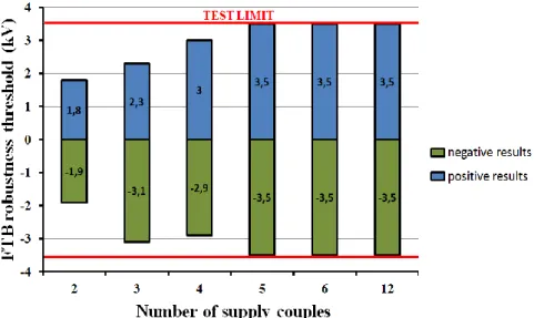
The influence of supply couples amount on the robustness results is measured by testing bonding diagram with the number of VDD equals to the number of VSS. Notice that supply couples are smartly placed around the chip (VDD wire is next to the GND wire and uniformly distributed) and no singular bonding diagram is tested with respect to usual rules. FTB test results are graphically represented in Figure 26.
With such results, it seems that the more supply couples there are, the more robust the microcontroller is. But to validate this hypothesis several placements for a given number of supplies will be tested.
Chapter 2 : Stress propagation mechanism understanding
- 30 -
Figure 26: Graphical representation of number of supply couples influence
1.1.3 The impact of the supply placement
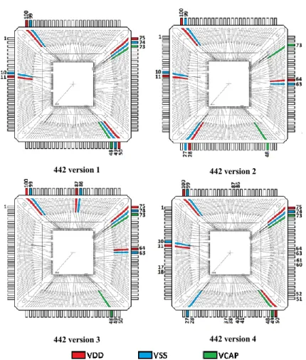
As there are 12 available supply pads on the chip, it is possible for low count supply couples, to change their placement. Bonding diagrams with the same number of supply couples are measured. The 442 configuration is chosen because its results on the previous test are under the maximum test limit. By this way, improvement or degradation would be observable. For supply placements described in Figure 27, singular placement like separated VDD and VSS (442 version 4) or non-distributed supply around the chip (442 version 3) are evaluated. Notice that the previous 442 bonding diagram corresponds to the version 1.
FTB test results are summarized in Table 5. The previous hypothesis regarding the number of supply requires a deeper analysis. Indeed, the supply placement has also a significant influence on the FTB robustness voltage threshold. It can change results positively or negatively.
Table 5: Supply placement influence test results
Bonding version FTBth+ FTBth-
442 1 3.0kV -2.9kV
442 2 >3.5kV <-3.5kV
442 3 2.2kV -1.3kV
Chapter 2 : Stress propagation mechanism understanding
- 31 -
442 version 1 442 version 2
442 version 3 442 version 4
Figure 27: Supply placement influence
1.2 Conclusion about results
The number of external capacitors, the number of supplies and the placement of those supplies are able to change the robustness threshold in a wide amplitude. Results provided by this study permit to affirm that the chip is not the only contributor to the FTB test robustness. The supply network and the bonding diagram in particular has a sensible effect on the robustness to FTB stress.
No clear rules can be extracted from this study. But classic design rules, such as mores supply pair as possible, GND close to VDD, supply distributed around the chip, are not enough to protect a chip from the FTB stress.
Beside those results which show that bonding diagrams impact the susceptibility, there is no reason that the PCB escapes to this rule. It is clear that
Chapter 2 : Stress propagation mechanism understanding
- 32 -
the supply network, including PCB, bonding wires and silicon, influence the stress propagation and its effect on the microcontroller behavior.
How does the stress go through this network from the injection point and disturbs circuits inside the die? Seeing results presented before, the hypothesis that fails are caused by the common mode to differential mode conversion seems to be the most obvious. This hypothesis will be explained in the next section.
2
Common mode to Differential mode
conversion hypothesis
This section is dedicated to the understanding of the common mode disturbance and its implication in the circuit disturbance. The mechanism which transforms the common mode stress into a differential stress will also be broached.
2.1 Common mode on supply
The particularity of the FTB stress is that it is a common mode disturbance. If it is applied on a device supply, the reference node (GND) and the power node (VDD) vary at the same time with the same amplitude with respect to the ground. It means that the device supplied between those two nodes sees the same voltage VDD – GND during all the common mode variation as shown in Figure 28.
Chapter 2 : Stress propagation mechanism understanding
- 33 -
A priori an electric device can’t be disturbed by a common mode disturbance on its supply if nodes impacted are its only references. This is the case of microcontrollers when only one supply is used. But this is not what is observed during a FTB test as the microcontroller fails anyway. This observed behavior leads to the following question.
How a common mode perturbation on supply can disturb an electronic device? A common mode stress can be transformed into a differential mode stress in certain conditions. This conversion will be explained in the following section.
2.2 Common mode to differential mode conversion
understanding
A common mode variation on supply cannot disturb an electrical circuit, only differential mode disturbance can impact its behavior. The hypothesis which follows from that, is this one:
The common mode stress is converted into a differential mode between the injection point and inside the die.
It is of course not possible if the supply network is considered as two perfect wires for the power and the ground. What if we consider imperfect wires for power and ground? To understand what happens, a simple model is proposed representing two supply wires. This model given in Figure 29 takes into account the resistance, the inductance and the capacitance of wires with respect to ground.
Chapter 2 : Stress propagation mechanism understanding
- 34 -
The signal VIN represents a common mode disturbance, the capacitive
coupler is not represented, and this is a AC simplified schematic. If R1 = R2, L1 = L2 and C1 = C2, voltages on A and B with respect to the ground are the same. VAB is constant, an IP supplied between A and B would see the same voltage.
If just one of R, L or C parameter is modified, voltages at A and B points are not the same anymore, VAB is not constant. By introducing a common mode
stress a differential variation appears. The Figure 30 show a simulation with only a difference on wires inductance. The first wire has an inductance of 20nH which correspond approximatively to a 2 cm length and the second 25 nH for a 2.5 cm length wire. The input signal VIN is a simple step.
Figure 30: Common mode into differential mode conversion
It is possible to make the same model with the order of magnitude of bonding wire in a QFP package. The inductance value is around 2nH for a QFP100 bonding wire and resistance approximately equal to 100mΩ. The capacitance of the VDD and VSS nodes with respect to the ground if the insulating plane of the FTB test bench is 10cm thick is around 10fF depending on the size of the chip (cf. Figure 17, page 20). In a QFP package the wire bonding length varies by 40% depending on their placement. In Figure 31 the differential voltage is plotted for L1 = 2nH and L2=2.5nH, which correspond to 0.5mm length difference, and a single stress amplitude of 1kV.
Chapter 2 : Stress propagation mechanism understanding
- 35 -
Figure 31: Common mode to differential mode conversion QFP order of magnitude
By modifying the bonding diagram, the way by which the common mode is converted into the differential mode changes. So the stress seen by internal IPs changes for each kind of bonding too. As it is a mismatch issue we can suppose that increasing the number of supply bonding wires only contributes, to average and therefor lowering the difference between paths.
Indeed, if the same kind of model is made with multi supply bonding wires instead of simple supply couple, it would give the circuit in Figure 32. To simplify it, only bonding wires are represented, but to be more accurate, the printed circuit board and the supply network on the silicon might be also modeled.
Figure 32: Simplified multi supply wire bonding model
There are still two paths from the signal generator to a point A and another to point B. But the number of influent parameters on common mode to differential mode conversion is much higher than with only two wires. Those
Chapter 2 : Stress propagation mechanism understanding
- 36 -
parameters depend on bonding wires length, wires height with respect to the ground plane, their geometry, and their material. It is almost impossible to have the same path from the signal generator to point A and B because of several reasons such as mechanic constraints for connections which induce tolerances, imperfections on materials and so on.
For the FTB test, all paths between the stress injection point and the supply points of a weak intern circuit have to be taken in account to understand a failure.
2.3 From concept to reality
A way to convert a common mode stress into a differential mode stress is identified. But imperfections of supply network such as capacitance or inductance have an impact which depends on frequency. The sensitive frequency range depends on the order of magnitude of those parasitic elements and so on the implementation of the supply network in the test conditions.
The next section is dedicated to the study of influencing parasitic elements of the supply network. It will lead to conclude if they are significant enough to provide a differential stress able to disturb circuits inside the chip in real conditions, and for which frequency range.
3
Main parameters on common mode to
differential mode conversion
A key factor on FTB test failure understanding is the common mode to differential mode conversion of the disturbance. The encountered phenomenon has been described in the previous part. The common mode to differential mode is caused by the difference between the VSS and VDD path from the stress injection point to the tested circuit. In a first time, the microcontroller is considered as the tested circuit. But a microcontroller is by itself a complex assembly of several circuits, so it is possible to consider one of those circuits as
Chapter 2 : Stress propagation mechanism understanding
- 37 -
the test target. By this way the internal parameters of the chip have also their contribution.
Influencing parameters will be studied from the bigger in terms of size to the smaller as illustrated in Figure 33.
Figure 33: Influencing parameters studying parts
Each part has its specificities and interacts with each other. No precise value will be given, but only the order of magnitude. Indeed parts of the test bench are handmade and subject to mechanical tolerance, and this study is intended to be as general as possible.
3.1 Test bench parameters
In this paragraph, the test bench refers to the stress generator, cables and the capacitive coupler. The test board, the package and the die will be studied in next parts. Formulae to calculate most encountered parasitic elements are also introduced in this section.
A schematic of the entire test bench is given in Figure 17 (page 20) and a simplified electrical equivalent schematic in Figure 19 (page 21). The capacitive coupler is considered as perfect and Lp protection inductors as an
open circuit for the stress. However, there are wires between the capacitive coupler and the test board which can be modeled with a RLC circuit as represented in Figure 34.

![Figure 24: ICIM-CI schematic extracted from IEC 62433-4 standard [22]](https://thumb-eu.123doks.com/thumbv2/123doknet/13183484.391392/38.892.273.611.108.509/figure-icim-ci-schematic-extracted-iec-standard.webp)