Capacitance
by
Albert C. Chow
B.S., Columbia University (1999)
Submitted to the Department of Electrical Engineering and Computer Science in partial fulfillment of the requirements of the degree of
Master of Science
at theMassachusettes Institute of Technology June 2002
© Massachusetts Institute of Technology. All Rights Reserved.
Author
Department of
Certified by.
Assistant Professor, Department of Electrical
BARKER MASSACHUSETTS INSTI V
OF TECHNOLOGY
JUL
3 1 2002
LIBRAR IES
Electrical Engineering and Computer Science
February 24, 2002
7
,David J. PerreaultEngineering and Computer Science Thesis Supervisor
7<
Accepted by
Arthur Smith
by
Albert C. Chow
Submitted to the Department of Electrical Engineering and Computer Science in partial fulfillment of the requirements of the degree of
Master of Science
Abstract
Switching power converters are widely used due to their excellent efficiency, but they inherently generate ripple. Passive low-pass LC filters have been traditionally employed to meet ripple and EMI specifications [1]. These passive filters can contribute
considerably to the volume and weight of a power converter. In particular, capacitors can become relatively large in order to meet strict ripple specifications. This is detrimental to cost and reliability of these passive EMI filters. For these reasons, capacitors in EMI filters can pose a considerable design challenge. Active circuit techniques can
substantially reduce passive EMI filter capacitor requirements. This thesis investigates using active circuitry to mitigate the challenges of designing with large capacitors on three fronts: reducing capacitance in EMI filters, reducing damping capacitance, and reducing capacitance cost.
A significant reduction of the passive EMI filter capacitor can be achieved by
active ripple filters. This thesis investigates a hybrid passive/active filter topology that achieves ripple reduction by injecting a compensating voltage ripple across a series filter element. Both ripple feedforward and feedback are employed. The design of sensor, amplifier, and injector circuitry for this application is explored. The experimental results demonstrate the feasibility and high performance of the new approach, and illustrate its potential benefits.
The damping capacitor can easily become the dominant capacitance of the system. By using signal-level transistors, the needed capacitance can be greatly reduced.
A feedback system using current sense and current drive is explored in this thesis. Test
results demonstrate an improvement by a factor of a thousand.
Active techniques can also reduce the cost of capacitor in EMI filters, by
enhancing the performance of low cost capacitors. This work applies active techniques to the input EMI filter of a commercial automotive motor drive system. Initial evaluation has demonstrated the feasibility of this approach. More work will be required to further evaluate the details of active filter system to this commercial application.
Thesis Supervisor: David J. Perreault
I would like to acknowledge the support for this research provided by the United States
Office of Naval Research and by the member companies of the MIT/Industry Consortium on Advanced Automotive Electrical/Electronic Components and Systems.
I owe a great debt of gratitude to my advisor, David Perreault, for his infinite patience,
for his kindness, and for his bountiful knowledge of circuits and life, which always brought a smile to my face and occasionally filled me with awe. Everything I know about power electronics and possibly circuits I learned from him. I would also like to thank Professor Kassakian and Dr. Keim, whose support and advice I value greatly. Special thanks to all my colleagues and friends in LEES, Ashdown, and other random places, without you, life at MIT would be boring. In the end, it is the times which I spent with all of you that I will remember.
I would like to dedicate this thesis to me, because I wrote it. On second thought, I would
1 Introduction
1.1 M otiv ation ... 1.2 A Feedforward/Feedback Active Ripple Filter...
1.3 A ctive D am ping... 1.4 Feedback A ctive Filtering... 1.5 Thesis Objective and Organization...
2 Voltage Injector Design
2 .1 Introdu ction ... 2.2 Single Magnetic Component Voltage Injector... 2.3 Two Magnetic Component Voltage Injector... 2 .4 C on clu sion ...
Active Circuitry Design
3 .1 In trodu ction ...
3.2 Feedforward Control Implementation...
3.2.1 Design of Summing Amplifier Using a Current Feedback Op-A m p ...
3.2.2 D esign Procedure...
3.3 Feedforward Control Analysis... 3.4 Feedback C ontroller...
3.4.1 Feedback Gain Amplifier... 3.4.2 Compensation Design Procedure...
3 .5 Su m m ary ...
Active Damping
4 .1 In trodu ction ... 4.2 Active Damping Design Considerations...
9 9 12 13 15 15 17 17 18 26 28 31 31 32 33 35 36 38 41 43 47 49 49 52 3 4
4.3 D esign Procedure... 56
4.4 Initial T est R esults... 56
4 .5 Sum m ary ... 57
5 Experimental Results 59 5.1 Introdu ction ... 59
5 .2 T est S etup ... 59
5.3 Experimental Results and Evaluation... 61
5.4 Design of a Comparison Passive Filter... 63
5.5 Design of a Complete Active Filter ... 64
5.6 Sum m ary ... 68
6 Application of Active Filtering to Motor Drives 69 6 .1 Introduction ... 69
6.2 Active Filter Design Considerations... 72
6.3 Amplifier Design Considerations... 75
6.3.1 Voltage Sense - Current Drive Topology... 76
6.3.2 Voltage Sense - Voltage Drive... 79
6 .4 Sum m ary ... 8 1 7 Conclusion and Future Work 83 7.1 Introdu ction ... 83
7.2 A ctive Filtering... 83
7.3 A ctive D am ping... 85
7.4 Active Motor Drive Filters... 85
7.5 Sum m ary... 86
INTRODUCTION
1.1 Motivation
Switching power converters inherently generate ripple, and typically require input and output filtration to meet ripple and EMI specifications, (e.g., Fig 1.1). Passive LC low-pass filters have traditionally been employed to achieve the necessary degree of ripple attenuation [1]. The capacitors in these passive filter components often account for
a large portion of filter size and cost [1-4]. Furthermore, the temperature and reliability limitations of filter capacitors can present a significant design constraint.
Take for example a commercial application, which uses a 1-kilowatt inverter for automotive electro-hydraulic power steering. The input filter for this switching inverter requires three electrolytic capacitors and two inductors. The capacitors account for
approximately 75% of the filter volume, and a rough estimate suggests that they attribute to more than 60% of the cost. Furthermore, there is the question of the lifetime of these
large electrolytic capacitors when they are subjected harsh environmental conditions (e.g. vibration and wide temperature ranges). Coupled with strict EMI requirements shown in Fig 1.1, techniques to reduce the required capacitance become attractive.
An alternative to the conventional passive filtering approach is to use a hybrid passive/active filter [2-10]. In this approach, a small passive filter is coupled with an active electronic circuit to attenuate the ripple. The passive filter serves to limit the ripple to a level manageable by the active circuit and to attenuate ripple components that fall beyond the bandwidth of the active circuit. The active filter circuit cancels or suppresses the low-frequency ripple components that are most difficult to attenuate with a passive low-pass filter. Essentially, the cut-off the LC filters needs to be placed well below the
SAE J1113/41 Class 1 EMI Specifications
80 ~ - -- ~ ~ -~ -- - -- -- ---I -- -- ---- --- -- I r -70 - - - - --40 0.1 1.0 10.0 100.0 Frequency (Mglz) FCC EMI Specification 70 --- -~*""---. _ ____ FCC Class A FCC Class B 50 --- --- - -- - --40 ___ 0.1 1 Frequency MHz) 10 100
Figure 1.1 Various EMI specifications: (from top to bottom) SAE Ji1113/41 Class 1 Automotive
conducted EMI specification for narrowband signals. FCC conducted EMI limits. The voltage is measured across a 500 LISN impedance.
frequencies that are to be attenuated, which make the components large. By using active circuitry to provide a fair amount of attenuation, less attenuation is required from the passive filter. This permits a substantial reduction in the passive filter size, with potential benefits in converter size, weight, and cost.
Active filters may be characterized by whether they inject ripple voltages [3,7] or currents [2,4-10] to achieve ripple reduction. Controls governing the ripple correction can be derived through either feedforward [2,9,10] or feedback [5-8]. Feedforward controlled filters sense a ripple component and inject its inverse, while feedback
controlled filters suppress ripple via high-gain feedback loop, see Fig 1.2. Combinations of these mechanisms are also possible (see [3,4] for example), and there are a wide variety of means for implementing the sensing and injection functions.
This thesis focuses on active filter techniques that minimize the required
capacitance in filters. A hybrid active/passive topology is introduced that achieves ripple reduction by injecting an opposing voltage in series with the voltage ripple source. This
z z Z
Power Power
Converter Load onverter Load
(noise K 4 (noise
source) source)
zZ Z
Power Power
Converter Load Converter Load
(noise A (noise
source) source)
Figure 1.2 Various active ripple filter topologies (clockwise from top left): Current ripple filter using feedforward control. Voltage ripple filter using feedforward control. Current ripple filter using feedback control. Voltage ripple filter using feedback control.
is effective in minimizing the size of EMI capacitors needed. A second hybrid
active/passive technique uses a current amplification topology to reduce the needed filter damping capacitor. Finally, the use of feedback active filters to reduce the filter capacitor size in PWM motor drives is explored.
1.2 A Feedforward/Feedback Active Ripple Filter
Figure 1.3 illustrates an active ripple filter topology using both feedforward and feedback. This topology operates by injecting ripple voltage to oppose the ripple voltage appearing across the buck capacitor Cb,,ck. Essentially this technique mimics a voltage divider. The voltage ripple is divided between the active voltage source and the output.
If the voltage source perfectly duplicates the voltage ripple then the output voltage will be
ripple free. The injector design is challenging since it must accurately generate the desired ac injection voltage while carrying the full dc converter current. The injection signal is based on a superposition of easily-measured feedforward and feedback voltage ripple signals. Implementing the control design is also a challenging task. The transfer
function from the ripple source to the output is given by equation 1.1 for a feedforward gain of K(s).
V0 (s)
Vrpe (S)= - K(s) (1.1)
V, (S)
ubuck
Figure 1.3 Feedforward / feedback voltage ripple filter used in combination with a passive filter at the output of a buck converter. The hybrid passive/active filter enables a reduction in the size of the passive filter components.
For a perfect feedforward path gain of unity, the ripple at the output would be zero. However, due to gain and phase accuracy limitations in the components, feedforward cancellation alone cannot fully attenuate the ripple. Considering the feedback path alone, the ripple source to output transfer function is:
V U1 (s) .1
Vrippe(S) 1+ A(s)
The ripple at the output becomes small as the magnitude of gain A(s) becomes large. In the feedback case, stability considerations limit the achievable feedback suppression. Combining feedforward and feedback takes best advantage of the injector circuitry and maximizes ripple attenuation. This thesis will explore this active/passive filter technique in detail. It will be shown that the proposed structure is attractive in cases where it is desirable to minimize the passive filter capacitance, Cu,.
1.3 Active Damping
Figure 1.4 illustrates how filter damping is often implemented. In many cases, passive components used to implement filter damping can be larger than the primary filter elements themselves. For instance, the capacitor value used in a shunt damping leg is
Lbig
R
out
Cbig
cout
Figure 1.4 Illustrates common damping topologies (from left to right): series damping and shunt damping.
The series damping topology employs an inductor and resistor. The DC current component flows through the output inductor. At higher frequencies the current flows through the resistor because the bypass inductor is smaller than the output inductor. The shunt damping approach uses a capacitor and resistor. At DC there is no voltage across the resistor. At AC frequencies near the corner frequency ripple flows through the resistor.
usually an order of magnitude larger than the value of the filter capacitor [1]. Active damping, in which active circuits are used to realize the desired damping characteristics, is an attractive approach for reducing passive component size.
Realizing active damping for a shunt damping leg suggest topologies where a damping capacitor is actively enhanced. Just as with active ripple filters, this can be accomplished in a variety of feedback topologies: current-sense/current-drive, voltage-sense/current-drive, current-sense/voltage-drive, and voltage-sense/voltage-drive (Figure
1.5). This thesis investigates the use of the current-sense/current-drive topology for
damping. It will be shown that the required size of the damping capacitor is greatly
lZ ZC Iz zc AA~s)Iz ZZ r Z ,, Z Z Z [1+)V AVs A+ sA(s) zZe Zeq z A(s) eq + -A(s)V, e CA(s) Z 1+ A(s)
Figure 1.5 Various impedance reduction topologies (clockwise from top left): Current sense-Current Drive. Current sense-Voltage drive. Voltage sense-Current drive. Voltage sense-Voltage drive.
reduced by the active circuitry. 1.4 Feedback Active Filtering
Capacitors contribute significantly to the cost of EMI ripple filter. High
frequency demands further exacerbate this cost. In other words, the cost to capacitance ratio increases for high frequency capacitors. For instance, ceramic capacitors are extremely expensive due to their excellent high frequency performance. Filter designs
still rely on relatively large ceramic capacitors in order to meet strict EMI specifications at high frequencies, which add to filter cost. This makes ceramic capacitors a prime target for active techniques.
Active topologies are used in conjunction with low frequency capacitors to mimic the performance of high frequency ceramic capacitors at a fraction of the cost.
Since the hybrid filter must replace an expensive ceramic, cost considerations severely constrain the design of the hybrid filter. The active ripple filter uses feedback control. Similar to active damping, the various topologies is shown in Figure 1.5. These active techniques are applied to a full production, commercial PWM motor drive. The thesis will explore the primary technical challenges and proposed topologies.
1.5 Thesis Objective and Organization
The thesis is organized as follows: The following two chapters of the thesis explore the design of the active ripple filter illustrated in Fig 1.3. Chapter 2 addresses the design of transformer-based voltage injectors and sensors. Chapter 3 explores the design of feedforward and feedback control circuitry for this approach. Active damping
techniques are addressed in Chapter 4. Chapter 5 of the thesis describes the application of the proposed scheme to the output filter of a buck converter, and experimentally
compares the performance of the approach to that achievable with a conventional passive filter. Chapter 6 explores the implementation of active ripple filter to PWM motor drives. Finally, Chapter 7 offers a conclusion to the work.
VOLTAGE INJECTOR DESIGN
2.1 Introduction
This chapter considers the design of voltage injectors for active ripple filters. The injector circuit (represented as a controlled voltage source in Fig. 1.1) must meet a
number of challenging requirements. First, the injector must carry the full de output current with minimal losses. Second, the injector must provide both isolation and sufficient input impedance for the active electronics. Finally, it must be able to replicate the injector signal with high fidelity. For the given constraints, a transformer proves to be an ideal choice for a voltage injection mechanism. Advantages of a transformer-based
injector include minimal dc losses and inherent galvanic isolation (for coupling to control circuitry.) Furthermore, for an ideal transformer the voltage appearing on the primary
Voltage Transformer Lp_ L Buck* N2 C out DC 6_ V Converter
High Pass Filter
Figure 2.1 Hybrid Active/Passive Filter implementation using a single-magnetic component voltage injector. Voltage is sensed with an op amp via a high pass filter. Voltage is injected using a voltage transformer; the significant transformer parasitics are shown. L,, is the magnetizing inductance, and L1 and L12represent the leakage inductances.
side is a perfectly scaled version of the voltage on the secondary side. This thesis considers two different voltage injector implementations that address these challenges.
2.2 Single Magnetic Component Voltage Injector
Figure 2.1 illustrates one possible transformer-based injector, including the relevant transformer parasitics. A primary challenge is handling the large de current in the system. In this case, the dc current of the converter passes through the magnetizing inductance of the transformer. This requires that the core be properly sized and gapped to prevent saturation under this heavy bias condition. The transformer magnetizing inductance L, and turns ratio must also be selected such that the transformer presents sufficient impedance so that the signal-level amplifier is not loaded. The amplifier circuitry is required to generate an ac voltage of magnitude:
N2
Vircuit = N (2.1)
and a current of magnitude:
'circuit - N1 Vrippie (2.2)
N2 CorippleL
where L, is the magnetizing inductance measured on the transformer's primary side, IVrippiel is the magnitude of the ripple to be cancelled, and 0
Oripple is the fundamental frequency of the ripple.
The first step in designing a transformer voltage injector is calculating the
required magnitizing inductance (and hence transfomer core size), which is determined by the output current and dissipation limits of the amplifer circuitry. The transformer turns ratio is used to match the voltage and current drive levels of the amplifier to those
required for voltage ripple cancellation. To maximize amplifier use and minimize injector size, the turns ratio should be selected to fully utilize the available amplifier voltage and current swing. For example, the amplifier in the prototype system has an output voltage limit of +/- 6 V, and a current limit of +/- 100 mA. To suppress a 2.4 volt peak-to-peak ripple voltage, a turns ratio of 1:5 is selected. Given a 125 KHz fundamental ripple frequency, a magnetizing inductance of 5 pfH is selected so that the current drive capability of the amplifier is not exceeded. The magnetizing inductance determines many of the characteristics of the transformer.
The transformer must be properly designed for the calculated magnetizing inductance, which depends on four parameters (as in an inductor): the number of turns
(N), flux density (B), core area (A), and current (I).
LP NBAC (2.3)
I
The number of turns, N, is determined by core characteristics. The saturation flux, B, and core area, AC, is a factor of the type of core chosen and the material. The current, I, is given by the particular application (the maximum current should be used) and therefore is set. Although not represented in equation 2.3, window size is a very important
parameter. All of the windings must be able to fit in the core. Each of these parameters are inter-related, thus a list of possible cores choices can be generated and evaluated for use.
The core material is selected in the second design step. It is determined by numerous factors; including cost, core loss characteristics, magnetic saturation limit, and permeability. Neglecting cost, high frequency core losses are the primary factor.
Excessive core loss will generate heat and more importantly cause the transformer to greatly deviate from its ideal behavior. In the prototype, a 3F3-ferite core was selected for excellent performance at high frequencies. The core material in turn determines what flux will saturate the material (Bsat). As the flux in the core approaches Bsat, the permeability decreases, the inductance decreases, and the core losses increase.
Therefore, the transformer should be designed to operate less than the saturation flux density. The prototype has been designed with a Bmax of 0.3 T.
From equation 2.3, having determined Bmax and I a list of cores can be generated
by varying N and A. The number of turns, N, and core area, Ac, is not completely
independent. The core size if determined by numerous factors, one of which is window size. The window size must be able to accommodate both the primary and secondary turns. The size of the wire is determined by the amount of current that the wires carry. As a rule of thumb, the maximum current density should not exceed 500 A/cm2.
Otherwise, there will be excessive losses and heating due to the resistance of the wire. The prototype system has a maximum of 14 A through the primary and 100 mA through the secondary. Therefore, 14 awg wire is used for the primary and 22 awg wire for the secondary (wire data is readily available [14]). The minimum window area needed is the number of turns of the primary wire times the cross-sectional area of the primary wire plus the number of turns of the secondary wire times the area of the secondary wire, all multiplied by a factor to account for the limited packing factor of wire in the window. As a rule of thumb, the total wire cross-sectional area should be multiplied by a factor of 1.5 to 2 to get the required window area; again, packing factor estimates are available [14].
turns, N, is determined. A set of viable cores is narrowed from this larger list by checking if all the windings are able to fit in the core window. To fully determine the characteristics of a core the gap size needs to be extracted.
The maximum flux sets the gap size. The amount of flux through a core is dependent on the number of turns, current, core area, permeability, and mean core length. The core area, permeability, and mean core length can be incorporated into one parameter denoted as AL, representing the number of nH per turn squared. Thus the flux is
determined by N, I, and AL. The flux B in terms of AL is given below:
B = NIAL (2.4)
Ac
The Bmax and I are predetermined and a set of Ac with corresponding N was found
previously, thus AL can be determined. This provides a set of possible cores with a given
N, core area, and gap size. AL and Ac are inter-related.
When selecting a particular core the tradeoff between gap size and core size must be considered. Equation 2.4 shows a couple of interesting relationships. For a given number of ampere-turns, the core area can be reduced if the Bmax is increased.
Alternatively, the core area can also be decreased if AL is decreased. This has the downside of increasing the leakage inductance which has detrimental affects on the
R
R
corei+R
Ni (Rair core
Rgap
Figure 2.2 A magnetic circuit representation of leakage inductance in a transformer. Flux is represented by current and reluctance is represented by resistance. As the gap increases, the resistance increases and more flux will travel through the air, causing more leakage.
system performance (discussed later). The increase in leakage inductance with reduced
AL (and larger air gap) is illustrated by the magnetic circuit in Fig. 2.2. AL is decreased by
decreasing the core permeability or increasing the air gap. As the gap increases, its resistance to flux increases, therefore causing a larger percentage of flux to bypass the core. Percentage leakage inductance is directly related to the fraction of flux that bypasses the core. Given the relationships of the main parameters, tradeoffs between different selections can be made.
Leakage inductances in the transformer affect the controls of the filter and
therefore play an important part in the design. The use of feedforward ripple cancellation requires that the ripple be both sensed and injected with great accuracy. Therefore, the injector must have negligible magnitude attenuation and phase shift for the frequency range of interest: any phase or magnitude error will greatly degrade the performance of the feedforward control. The signal fidelity of an ideal transformer is perfect. However, transformer parasitics [11,12] (illustrated in Fig. 2.3) can limit the injector performance. Experimental results have verified that the primary-to-secondary shunt capacitance,
Cshunt, can be neglected for converters operating at up to several hundred kilohertz,
because it does not affect the behavior of the injector for the frequency range of interest.
L1:
L1
V .LVprimary
psecondary
However, the secondary side (amplifier-side) leakage inductance, L12, forms a voltage
divider with the magnetizing inductance reflected to the secondary side, resulting in a magnitude error. A transformer design that minimizes percentage leakage inductance is advantageous.
Leakage inductance also affects the stability of the feedback control. Stability is the major factor limiting achievable attenuation. The injector transformer is in the feedback loop, so any phase lag added by the transformer can greatly decrease stability. An ideal transformer adds zero phase lag, but the parasitic inductance on the primary side (injection), L11, plays a surprisingly important role in the stability of the system. As will be described in chapter 4, L11 and the output capacitor, Cour, form a 2nd order low-pass filter, and the phase shift associated with this parasitic filter can affect the stability of the feedback control. As a result, the transformer design should also minimize L11 to ease the
constraints on the control design.
Topology Primary Over Secondary Interleaved Litz Wire Secondary Over Primary Secondary
Over Primary Description 0 P0 P0 oP0 0 0 0 0 P 0 p 0 M 0 0 0
Manufacturing Low Low Medium High
Difficulty
[Lp (pH) 4.92 4.86 4.82 4.68
Lii (pH 0.13 0.12 0.04 0.07
L2 (H 0.34 0.75 2.45 0.78
Table 2.1 Characteristics of different transformer winding topologies. The description row illustrates the winding geometry, showing half of the bobbin. The large circles represent the primary winding and the smaller circle represents the secondary.
It is advantageous for both feedforward and feedback control to minimize the leakage inductances, which depends on two factors: winding geometry (as mentioned above) and core gap length. Reducing gap size will reduce the leakage inductance, but it substantially increases transformer size. For a given current, magnetizing inductance, and maximum allowable flux density, there is a direct relationship between AL
(inductance factor, nH/turns2) and core area, A core:
A core - 'p,maxXLAL (2.7)
Bmax
AL is inversely proportional to the gap length, which typically correlates with leakage
inductance. Thus, there is a tradeoff between the leakage inductance and the core size. Leakage inductance can be further reduced by finding a beneficial winding geometry.
Various winding geometries are investigated in this thesis, bearing in mind the constraint of manufacturing ease. Leakage inductance stems from imperfect coupling, where the flux generated by one set of windings does not link the other set of windings. Winding topologies that have the windings close together are advantageous. Topologies where the windings are interleaved and placed on the same magnetic component are
Impedance at the primary Impedance at the secondary Impedance at the primary side with the secondary side side with the primary side side with the secondary side
shorted open open
L12 L
11
primary L secondary V L
V. L1/N N2L Vprimary
Z3=L12+L2 /N2 Z2=LI2+N2L, Z1=Lil+L,
Figure 2.4 A method for measuring leakage inductance. Three measurements are made (as illustrated n the three columns). The magnetizing inductances and both leakage inductances can be estimated from these measurements.
investigated further. Table 2.1 illustrates the experimental evaluation of a number of possible winding arrangements. The winding geometries and corresponding leakage inductances are show. The leakage inductances can be calculated from various measurements on the primary and secondary side, as illustrated in Fig. 2.4. After comparing several geometries, while keeping implementation ease in mind, an
interleaved primary over secondary winding method was selected for the prototype, as
this resulted in a low value of L12.
Given these relationships various tradeoffs must be made in the core selection. For instance, the prototype injector could be implemented using a RM14 core with a relatively small gap and low leakage. Given the required primary side inductance and
current following equations illustrate some of the previous tradeoffs:
L = ALN 2 (2.5)
L = core max (2.6)
2 Imax A L
A RM12/I core was selected with an area of 146 mm2. A standard gapped core with an
AL value of 315 nH was chosen, resulting in four primary turns and twenty secondary
turns. This results in a primary side leakage (L11) of 0.156 ptH (3.4%). The secondary
side leakage (L12) is 2.3 pfH (2.5%). The corresponding attenuation of 0.98 is calculated
from equation 2.4.
Attenuation = LU ' (2.8)
L +N 2 LU V(
To the extent that this attenuation is known and repeatable, it can be compensated for in the control design.
2.3 Two Magnetic Component Voltage Injector
An alternative method for implementing the injector is to use a bypass inductor in parallel with a high-frequency transformer, as illustrated in Fig. 2.5. In this approach, the bypass inductor, which is implemented with a gapped core and wound with large-gauge wire, serves as the dc bypass element. This function is accomplished by the magnetizing inductance LP in the previous case. The high-frequency transformer is implemented with a much smaller ungapped core using small-gauge wire. This element serves as the means for voltage injection. The relative winding resistances determine the dc current sharing between the inductor and the transformer, while the ac characteristics are determined by the relative inductances. This topology essentially de-couples the inverse relationship between leakage inductance and core size.
The design of the inductor and transformer is similar to the previous design of the transformer. In the bypass inductor implementation, the smallest core area should be selected because the inductor leakage inductance does not affect the filter performance. The transformer implementation is also the same except it must be implemented with an ungapped core to keep overall performance comparable to the single-core
implementation. Furthermore, the magnetizing inductance must be at least ten times that of the bypass inductor, which remains at 5pfH. This is due to the AC performance; at the frequencies of interest the parallel AC impedance of the bypass inductor and the
magnetizing inductance must equal 5tH. Once again the winding topology is important in minimizing parasitic inductances' (see table 2.2), which affect performance. The attenuation of the voltage injected with this approach may be calculated as:
N
2 L L VAttenuation = U ( DC ) _ out
N2
L
+ L 12 Ll + LDC V(.
By minimizing the leakage inductances, L,1 and L,2, the attenuation is minimized. It
should be noted that in the previous case, only L,2 caused a magnitude error in the
injected signal. In the two-core approach, Li1 also causes a magnitude error because it
forms a voltage divider with the bypass inductor. This approach can thus lead to a larger magnitude error.
A prototype ac transformer (with a 50pfH L,,) was wound on a non-gapped RM5
core, while the bypass inductor (5pfH) was wound on a gapped RM10 core. The
combined volume of the inductor and transformer is 4884 mm3. The single-core design
has a volume of 8340 mm3. The two-component approach thus yields almost a 50% reduction in total volume. The ac transformer magnetizing inductance L, is 50 pH, L11 leakage is 0.148 [tH (or 0.4%) and the L12 leakage inductance is 1.32tH (or 0.15%). This
is much lower than in the previous design. However, the attenuation is increased to 0.92,
1 The previous method of measuring parasitic inductances is not accurate in this case. Due to the increase in the number of turns, the shunt capacitance is larger. When the secondary side is shorted, a capacitive component appears on the primary side impedance. The previous method assumes no capacitance. To measure leakage, the attenuation from primary to secondary must be measured by driving the transformer
Topology Primary Over Secondary Over Interleaved
Secondary Primary Secondary Over
Primary Description P S S s s P S P SS P SS P s P S S P S S S P S P SS P SS P S S P SS P S S S P S P S S P SS p S S P S S P SS P 5 P S S pS S P SS P ZnS S p S pS5 p pSS
Manufacturing Low Low Low
Difficulty
L 38.83 41.36 48.23
L, (pH) .15 2.75 -2.8*
L12 (pfH) 1.32 2.77 -1.06*
* Not a negative inductance. Due to measurement errors. Larger shunt capacitance affects measurement models.
Table 2.2 Characteristics of different winding topologies. The figures illustrate the winding geometry. (Half the bobbin is shown.) The primary and secondary wire sizes are the same. The primary is denoted with a P and secondary with a S.
as compared to 0.98 yielded by the single-core design. The example confirms a volume versus gain tradeoff with the two magnetic component implementation in comparison to the single magnetic component implementation.
2.4 Conclusion
Transformer based implementations are well suited to the design challenges of a voltage injector. A primary constraint is handling the large DC current in the system without significant dissipation. Two implementations were introduced that overcame this constraint. The first passes the DC current through the magnetizing inductance of the injection transformer. The second uses a discrete bypass inductor. The voltage injector must also isolate the active circuitry from the power system; transformers naturally achieve galvanic isolation. For control considerations, the voltage injector should have high
with an AC source and measuring the open circuit secondary side voltage. Attenuation = N*Lp/Z2; Z1 and
fidelity. Different winding topologies are investigated to minimize parasitics that affect system operation. A simplified design procedure was introduced to design the proposed transformer:
Step1: Determine the desired voltage ripple to be canceled. Determine the maximum current and voltage of the active circuitry.
Step 2: Determine the turns ratios and inductance from equations 2.1 and 2.2.
Step 3: Select the core material base on individual constraints, including high frequency
performance of the material. Material selection determines the maximum core flux.
Step 4: Use equations 2.5 and 2.6 (with the constraints of current, inductance, and
maximum flux) to generate a list of possible core sizes, turns, and gap sizes. With the relationship of gap size (and hence core size) and transformer leakage inductance in mind, select an appropriate core.
Step 5: Choose a winding topology that will minimize parasitic leakage inductances. A
ACTIVE CIRCUITRY DESIGN
3.1 Introduction
The design of the active circuit is greatly dependent upon the frequency band over which the active filter must operate. For a dc/dc converter, the frequencies of interest include the fundamental switching frequency and beyond. Achieving significant attenuation at very high frequencies (e.g., beyond 10 MHz) is difficult and is better handled with purely passive attenuation. The example power converter considered in this thesis has a fundamental switching frequency of 125 KHz. Therefore, its pass band should include 100 KHz and beyond.
For a multi-stage amplifier implementation, minimizing the number of stages is beneficial in terms of cost and reliability, and facilitates the design of the feedforward and feedback controller. Feedforward control depends on the ability to amplify signals with high fidelity. Each amplifier stage introduces noise and parasitic capacitance, which distorts to the feedforward signal. The feedback controller needs to have a stable loop
Feedforward
Input Power Gain
Feedback Input
Feedback Feedforward
Gain Gain
Figure 3.1 A block diagram representation of the multistage amplifier. A three-stage amplifier structure is employed, comprising a feedback stage, a feedforward stage, and an output (power gain) stage.
response. Adding additional stages adds gain, but at the penalty of adding poles due to both amplifier dynamics and parasitic capacitances between stages. These parasitic poles can contribute to phase shifts near the unity gain crossover frequency, hurting phase margin (stability). Thus, the design objective is to achieve the necessary gain and bandwidth using as few amplifier stages as is practical. The design considered here is implemented with a three-stage amplifier structure: a power gain stage, a feedforward stage, and a feedback stage (see Fig 3.1). A high-speed buffer, LM6121, is used to implement the power gain stage. It is able to provide +/- 100 mA of current with +/- 6 volt output swing at a bandwidth of 50 MHz. This particular component was chosen because of its large bandwidth. Smaller bandwidths would lead to distortion caused by the dominant pole.
3.2 Feedforward Control Implementation
To obtain a three-stage design, the feedback-summing junction and the feedforward gain stage, illustrated in Fig. 3.1, are combined. The feedforward controller must be implemented with exact gain, minimal phase shift, and low distortion over the frequency range of interest. The desired gain of the feedforward path is equal to the injector turns ratio divided by the attenuation caused by the transformer parasitics:
Gainsinge N2LU + L11 (3.1)
NLU
Gainwo = N2L ±L 2 ( +LDc) (3.2)
NLU LDC
This way, the feedforward gain can be used to compensate the magnitude error due to transformer attenuation. In the prototype system, the single-core injector transformer
Feedforward 190 Q LM6121 Feedback --- 1 Ip 1k LTk2 I k --- LM6361 k00k 190 Q 1F60QY I I k Ip 800Q 180pF
Figure 3.2 A three-stage amplifier implementation of control. (From top to bottom and left to right.) The first stage
provides the power gain to drive the injector transformer. The second stage serves as the feedforward gain and the summing point for the feedback control. The last stage is the feedback gain with minor-loop compensation.
requires a feedforward gain of 5, while the two-component injector requires a gain of 5.2, since its attenuation is larger. It is important to note that manufacturing variations can make this gain compensation challenging, particularly for the two-component
implementation. The prototype amplifier design, illustrated in Fig. 3.2, uses readily available discrete components.
3.2.1 Design of Summing Amplifier Using
a Current Feedback Op-Amp
A current-feedback op amp is used for the feedforward gain because it achieves
the necessary gain, bandwidth, and slew-rate requirements for this application. The feedforward op amp also acts as a summer, which allows this stage to incorporate the feedback control signal. Current feedback op amps offer several advantages over the traditional voltage feedback op amps, but the design is more constrained. First, current feedback op-amps do not have a gain-bandwidth product limit. In other words, the -3 dB
point does not vary much as the closed loop gain is varied, unlike voltage feedback op-amps in which bandwidth decrease with an increase in closed-loop gain. Second, current feedback op-amps typically have a larger slew rate. These advantages come with the penalty of an increase in design difficulty. Therefore, the use of these op-amps in the prototype is limited to basic gain configurations using a purely resistive feedback loop. Capacitive feedback networks are possible, but the compensation is difficult. A further constraint requires the feedback resistor to be set by the capacitance in the load of the current feedback op-amp. Although there is no gain-bandwidth limit, the bandwidth is slightly degraded with increasing gain. Thus, in the stage which combines the
feedforward and feedback signals it is advantageous to make the gain for feedforward and feedback signals the same (equal to the desired feedforward gain); a separate gain stage will be added for the feedback control.
Several basic op-amp summing topologies are available for the stage which combines the feedback and feedforward control signals. Possible configurations include a: non-inverting summing amplifier (eqn 3.3), inverting summing amplifier (eqn 3.4) or a difference amplifier (eqn 3.5) (see Fig 3.3).
R+ Reedback Rfeedforward
R Rfeedback + R feedback R + R Vfeedfrward (3.3)
R R
out R f"edback + R f ,kedforward (3.4)
feedback feedbadforward
2 ) Rfeedward feedback)
Each of these topologies has its limitations. In the non-inverting configuration, the loop gain, which affects the bandwidth, is set by the Rf term. From eqn 3.3, the loop gain of
the op-amp is attenuated by the feedforward and feedback resistors; therefore the loop gain needs to be larger for a given gain. Increasing the loop gain will decrease the bandwidth. For the inverting configuration, the feedback and feedforward resistor is set
by Rf for a given gain. Thus the input impedance for both the feedforward and feedback
path is constrained to a relatively low value. For the prototype system, a difference amplifier is implemented. The difference amplifier allows the feedforward and feedback gain to be equal with out attenuating the loop gain. Although the feedback input
impedance is set by Rf, this configuration allows the feedforward input impedance to be set independently. This topology is advantageous because it provides this extra degree of freedom.
3.2.2 Design Procedure
The design procedure for the difference amplifier is as follows: The first step is to determine the load capacitance of the difference amplifier, which corresponds to the input capacitance of the power gain stage and parasitic capacitance. This capacitance
determines the value of feedback resistor. The estimated input capacitance of the
LM6121 power gain amplifier is about 3.5 pF. The number is rounded up to about 10 pF,
Non-Inverting Summing Amplifier Inverting Summing Amplifier Difference Amplifier
Rf Rfdbk R\^ Vfeedba R2 Rfeedback v vfeedback L---' d o~ut (Vd k + V-- Rout Rffeebac outI
Redak Vfeedfo ard ReRdfonvard
Vfeedforward
feedback
Figure 3.3 Various summing topologies (from left to right): non-inverting summing amplifier, inverting summing amplifier, and difference amplifier. In the non-inverting configuration the bandwidth is reduced. The inverting summing amplifier has low input impedance. The difference amplifier has low feedback input impedance.
to account for board and layout capacitance. From the data sheet, this results in a 1K feedback resistor.
Next, the feedback resistances can be determined, which affect the input
impedances of the difference gain block. The input impedance for the feedforward input
is R1+Rfeedfonvard. The input impedance of the feedback stage is R2. The input impedance
of the feedforward signal determines the size of the capacitance needed to sense the signal; more will be mentioned about this later. The prototype uses the minimum feedback resistance of 1K. Therefore R, and R2 are 190 ohms; and Rfeedback is 1K.
Finally, care must be taken to ensure that the power supplies are stiff. In other words, the amplifier power supply voltages must be constant with varying signal
amplitudes and frequencies. This can be easily accomplished by placing decoupling capacitors across the power supply very close to the amplifier. In the prototype a large-valued tantalum capacitor is used in parallel with a small ceramic capacitor.
3.3 Feedforward Control Analysis
There are two main limitations that dominate the feedforward system: non-exact gain compensation and nonzero amplifier output resistance. Due to parameter variations of the inductor and transformer, the feedforward gain cannot completely compensate for the magnitude error. Assuming zero phase error, the percentage error in magnitude
corresponds directly to the percentage of residual ripple. For example, a 10% magnitude error results in a 10% residual ripple. The phase error is also proportional to the residual ripple. The nonzero output impedance of the power gain stage, Ro,, causes a phase error, because it forms a high pass filter with the magnetizing inductance on the secondary side of the transformer (see fig 3.4):
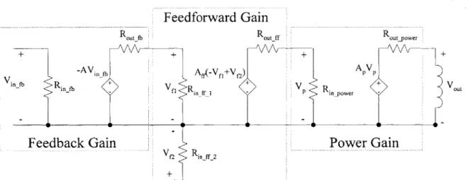
Feedforward Gain
R out fb R out ff Rout_power
-AViA-V+) A V
V
n~inffb R y RV Rinpower "
Feedback Gain Power Gain
Figure 3.4 The three stage amplifier with input and output impedances. There is a significant voltage divider between the feedback gain and the feedforward gain stages. A high pass filter is formed at the output.
Vran~sormer sN2 LU
(3.6)
Vircuit Rou, + sN2 Lu
For perfect gain, the percent residual ripple depends on the phase error
#
in the following manner:%Vesidual =100 * (1 - cos )2 + sin 2 yO (3.7)
The pole associated with the output resistance and magnetizing inductance is at 6.4 KHz in the prototype. Although it is well below the fundamental frequency, there is a slight phase shift of three degrees at the switching frequency. This results in a maximum 95% ripple cancellation by the feedforward system, as per eqn 3.7. The corresponding
+ Vinject
-+N C
L 20
AV
Figure 3.5 The left diagram shows the circuit representation of the feedback loop. The diagram on the right
depicts a block representation of the proposed feedback loop. The performance of the feedback controller is directly proportional to the gain, A (s).
magnitude error is negligible given knowledge of the transformer parasitics. Therefore it is these errors in magnitude and phase that prevent perfect ripple nulling.
3.4 Feedback Controller
Figure 3.5 shows the proposed feedback system. The design of the feedback controller is not only dependent on the switching frequency, but also on the stability of the control loop. The effectiveness of feedback control is directly dependent upon gain. Thus maximizing gain, without instability, is most desirable. As mentioned in section 2.2, the injector transformer leakage inductance LI, and the output capacitor Cu, form a low-pass filter, illustrated in Fig. 3.6. This two-pole filter causes an additional -180 degree phase shift from Vijec, to Vsense. Neglecting damping and assuming that the buck capacitor is nearly ac ground, the following equation gives the transfer function from the injected voltage to sensed voltage:
Hinjectr(VS) = Vsense (s) - 1
Vinject (s) 1 + (LCOU )s2 (
The higher the unity-gain crossover frequency of the loop gain, the larger the attenuation
V.
sense Rload
C ,
Figure 3.6 A circuit represention of the voltage injector loaded with the output capacitor. The voltage source represents the injected signal on the voltage transformer internal to the leakage inductance. To simplify the analysis the buck capacitor and the damping due to RIoad has been neglected. The feedback signal is sensed across the output capacitance.
will be across the frequency range of interest. However, if the -180 degree phase shift occurs at or before the unity-gain crossover, then the system will be unstable. The parasitic low-pass filter in the prototype occurs at around 1.5 MHz, therefore restricting the gain across the frequencies of interest, in this case from 125 KHz to 1 MHz.
The narrow frequency range is insufficient for this application. To overcome this limitation, a small inductive element, Lcomp, is added between the sense point and the load, see Fig. 3.7. In the prototype system this was implemented as a small magnetic bead. This results in the addition of two zeros after the two poles:
Vsen, (s) -(LCOmPCout )s2 -1
Hcomp, S in(s== Vinject (s) (3.9)
s 2 (Lcomp + L11 )Co, + 1
If Lcomp is much smaller than Ll, then the zeros occur just after the poles. Therefore the
phase of the system approaches -180 degrees (never reaching it due to damping) and then
returns to zero degrees. Figure 3.8 shows the frequency response of Hompinj(s) for the
prototype system.
The attenuation of the ripple will be greatly degraded at the frequency where the
V.inject
V R
sense 'sload
Cou
Figure 3.7 A circuit represention of the voltage injector loaded with the output capacitor and series compensating inductor. The voltage source represents the injected voltage. To simplify the analysis, the buck capacitor and the damping due to RIoad has been neglected. The feedback signal is sensed between the two inductors.
minimum of the magnitude response occurs. Furthermore, the ripple at this frequency is greater with feedback filtering than without. This is because not only is the magnitude at a minimum but the phase is nearly -180 degrees, which makes the gain, A(s), a negative number less than one, thus causing the attenuation to become less than one. These poorly damped pole and zero pairs make the design of the feedback control loop difficult.
One solution is to add additional series or shunt damping. In either case, resistive damping needs to be added on the load side of Vsense of Fig. 3.7, thereby allowing a
damping term for both the zero and the pole. A shunt damping leg is chosen for this particular application because it can be easily and inexpensively implemented with a
Bode Plot of Compensated Injector
-14.6 ---14.8 -.- 15.0 -15.2--15.4 -15.6 ~ 15.8 ; -16.0 -16.2 16.4 -16.6 -16.8 10 U1 IL 0 --20 --40 --60 --80 --100 --120 --140 --160 - -180-Limited -Two Poles
7
----
----.
L-A Two Zeros
0 1000
Frequen cy (K H z)
Phase Response of Compensated Injector
--- - --- ,--- - -- - --- --- -- --- --- --- --- --- -- ---- --- -- -- --- ---100 Two Zeros - ---- ---- --- - -1000 Frequency (KHz) 1 00co 10000
Figure 3.8 The transfer function from injected to sensed voltage. The two poles are due to the low-pass filter formed by Lij+Lcom, and C, adds a -180* phase shift. Lomp adds the two zeros and Co,, brings the phase back to 0*. The magnitude shows peaking near the poles and zeros of the system, which is due to limited damping.
capacitor and resistor. Simulations demonstrate that a 1 pF capacitor in series with a 0.5
Q resistor provides ideal damping. The implementation of the damping leg uses a 0.22 Q
resistor instead of a 0.5 Q to account for the ESR of the 1 pF capacitor. A series damping topology would require an inductor in parallel with a resistor. The inductor would be required to withstand the large bias current, thus making it large. This problem is similar to the one faced in the design of the transformer. As will be discussed in the following chapter, both damping schemes can also be implemented with a simple active circuit.
3.4.1 Feedback Gain Amplifier
The feedback amplifier block needs to be designed with large gain and
bandwidth, to maximize the effectiveness of the feedback controller. Furthermore, an op-amp with a basic, second-order frequency response with a dominant pole will facilitate the stability and compensation design. It is for this reason that a current feedback op amp was not chosen to implement the feedback block. The current feedback op-amp has a large, negative phase shift with small amplitude attenuation when it reaches its
bandwidth. This particular response is indicative of either a time delay or a large number of poles at frequencies slightly beyond the -3dB bandwidth. A high-frequency voltage-feedback op amp, LM63 61, is used for the voltage-feedback amplifier because it has a predictable attenuation and phase shift.
The overall topology of cascading the feedforward stage and the feedback stage leads to a tradeoff between feedback gain and feedforward signal noise. This relationship stems from the input impedance of the difference amplifier. The feedback gain block has non-zero output impedance, which forms a voltage divider with the input impedance of the difference amplifier as illustrated in Fig 3.4. The difference amplifier has relatively
small input impedance, 190 ohms, therefore the attenuation is significant. Thus the maximum gain of the added feedback gain stage is limited, and consequently the gain of the feedback loop is limited. Based on PSPICE simulations, the maximum open loop gain in the proposed configuration is around 100. In order to increase the input impedance the feedback resistor must be increased on the difference gain block. For current feedback op-amps, this increases the noise in the signal. The added noise only
(A) buck feedbackIV (active)
1. OH _ - __ 1. 0_ Al- 42.763M, 5.0665 A2 - 41.8101. -249.488 dif- 945.368K, 254.555 100rmV__ V (buf f out) Od-500 1. 0jHz 10mHz 100mHz 1L0Hz 10Hz 100Hz 1.CKHz 10KHz 100KHz 1.ONHz 1OMHz100HHz L2 P?(V(huff ut)
Figure 3.9 Simulation of the open ioop frequency response of the multi-stage amplifier. The unity gain cross over of 42 MHz and phase of -250 degrees is shown.
affects the feedforward controller because it relies on high signal fidelity. On the other hand, the noise in the feedback control is reduced by the loop gain. Even with this relationship, the cascade provides some advantages in minimizing the number of stages. The prototype attempts to minimize feedforward noise and therefore has a maximum overall feedback gain of 100.
3.4.2 Compensation Design Procedure
A compensator must be added to ensure feedback loop stability, which can be
implemented as minor loop compensation. Phase margin serves as a measure for the degree of stability. Phase margin is defined as 180 degrees minus the phase at unity gain cross over. As a rule of thumb, the phase margin should be at least 45 degrees.
Gain Compensation
Grn=12.C44 803 (at 3.Itt3e,007 radisec7, PIm:58.565 dkg. (at -.:I11 -(W0 0081007
0- - -
---I
Leg Compensation
Giai-13.004 dB tat 3. IZ24a.007 rad'bc), Prn=55S27d 2i .0347e+007 maOwro
i1
50
A 00 .
207R .
-OX1 7-40
Frequency (rad/sec) Frequency (rad/sec)
Lead Compensation Minor Loop Compensation
Gm=7.5451 dB (at 5.8523e.007 d/sec) Pm=57.059dg d A 3.1058+007 rad/seo) Gar-10.522 dB (at 4,5533e+007 rad/sec). Pmr79,17 deg. (at 4989e+007 radtec)
-2V
-2-Frequency (rad/sec) Frequency (rad/sec)
Figure 3.10 (Clockwise from top left) Various compensation techniques. Gain Compensation. L Compensation. Lead Compensation. Minor Loop Compensation.
I S
The first step in selecting a unity gain frequency is to determine the frequency response of the open loop system. Assume for now that the transformer and output capacitor add no phase shift, so the phase is primarily due to the multi-stage amplifier. Any phase error due to the passive components can be accommodated by a larger phase margin. The frequency response can be measured experimentally, simulated, or
approximated from the data sheets. From simulations (see Fig 3.9), the unity gain frequency is around 40 MHz and has a phase of -250 degrees, which makes the closed-loop system unstable. The closed-loop can be stabilized if the open closed-loop gain is shaped by a compensator.
The next step is to select a compensation method that allows the system to meet the determined crossover frequency and phase margin. The feedforward gain stage, power gain stage, and the transformer have a combined gain of approximately one and marginal phase shift below 10 MHz. Therefore, the entire system will be stable if the feedback gain block is designed with a unity gain crossover of 10 MHz and a phase margin of at least 85 degrees (this is the phase margin of the feedback stage alone). After the unity gain frequency has been selected, the problem reduces to the compensation of a single op-amp. Below is a list of possible compensation methods and their tradeoffs, see Fig. 3.10:
Gain compensation - Reduce the gain across all frequencies without affecting phase
Advantages - Easy to implement
Lag compensation - A zero is followed by a pole. The gain at frequencies beyond the
pole is decreased allowing the frequency response to cross over sooner. The zero is added to offset the negative phase shift added by the pole.
Advantages - Only lose high frequency gain
Disadvantages - Adds a small amount of negative phase
Lead compensation - A pole is followed by a zero. Adds a phase bump.
Advantages - Increases the phase at crossover
Disadvantages - Increases the crossover frequency, which may affect high frequency noise. As a rule of thumb, the maximum phase bump is around 60 degrees. Therefore, it may be
Ri
R2 ,C
R
Gain vs Frequency of Op-amp
80 60 5 0 -- - - - - - - - -- -4 0 --- ---S30 30 - - --10 --
-20-1.0E+03 1.0E+04 1.0E+05 1.OE+06 1.0E+07 1.0E+08 1.OE+09 Frequency (Hz)
Figure 3.11 Op-amp implementation of minor loop feedback. The gain vs. frequency of the amplifier in open loop configuration verses minor loop configuration is shown.
necessary to decrease the gain in order to meet phase margin specifications.
Minor loop compensation - Compensation is added to the feedback network of the op-amp. Advantages - A combination of lead and lag compensation can be implemented
Disadvantages - More difficult to implement.
The prototype uses minor loop compensation. For minor loop compensation the frequency response can be approximated by plotting the lower value of the open loop transfer function and the feedback impedance. The feedback impedance has a resistor in parallel with a series connection of a resistor and a capacitor (see fig 3.11). The impedance has a zero followed by a pole. The lower curve has a pole followed by a zero followed by a pole as the frequency increases (see fig 3.11). This forms a lag-lead compensator.
Intuitively, at lower frequencies the gain is set by R1. As the frequency increases, the
capacitor impedance decreases, which causes the feedback impedance to decrease. Thus the gain decreases. The minimum gain is reached when the capacitor shorts leaving R1 in
parallel with R2. As the frequency is further increased, the op-amp bandwidth is reached
and the gain is further reduced. The placement of the zero and pole are related. Placing a zero right at the crossover frequency has the advantage of maintaining the crossover while adding a slight phase bump. Knowing that the frequency response will crossover with a slope of 20 dB per decade, the position of the pole can be determined. With a gain of 100 and a zero at 10 MHz the pole must be placed at 100 KHz (from eqn. 3.10)
Cozero Gain
(3.10)