Design of a Wideband,
100 W, 140 GHz
Gyroklystron Amplifier
by
Colin D. Joye
MASSACHUSETTS INSTiTUTE OT TEGCLOGY2004
UBRARIES
B.S., Electrical Engineering and Computer Science (2002)
Villanova University
Submitted to the Department of Electrical Engineering and Computer
Science
in partial fulfillment of the requirements for the degree of
Master of Science in Electrical Engineering
at the
IASSACHUSETTS INSTITUTE OF TECHNOLOGY
September 2004
@
Massachusetts Institute of Technology 2004. All rights reserved.
Author ...
...
...
Department of Electrical Engineering and
Certified by...
6'
Computer Science
igust 6, 2004
Richard J. Temkin
Senior Research Scientist, Deptartment of Physics
Accepted by ...
Arthur C. Smith
Chairman, Committee on Graduate Students
Department of Electrical Engineering and Computer Science
uK
Design of a Wideband, 100 W, 140 GHz Gyroklystron
Amplifier
by
Colin D. Joye
B.S., Electrical Engineering and Computer Science (2002)
Villanova University
Submitted to the Department of Electrical Engineering and Computer Science on August 6, 2004, in partial fulfillment of the
requirements for the degree of Master of Science in Electrical Engineering
Abstract
The design study of a 140 GHz, 100 W continuous wave gyroklystron amplifier is presented. The device is intended for use in Dynamic Nuclear Polarization (DNP) enhanced Nuclear Magnetic Resonance (NMR) spectroscopy experiments. The gy-roklystron has five cavities and operates in the TE(0,2) mode with a low power elec-tron beam. The design was performed using MAGY, a nonlinear code for modelling gyrotron devices. The design process of the gyroklystron starting from the linear theory to the optimization of the final design in MAGY has been described in detail. Stagger tuning was employed to broadband the device. The design yields 130 W peak power, 36 dB saturated gain, and a -3 dB bandwidth of over 1 GHz (0.75%) with a
15 kV, 150 mA electron beam having a beam pitch factor of 1.5, radius of 0.64 mm
and calculated perpendicular momentum spread of 4%. Preliminary designs of the Magnetron Inject Gun (MIG), the input and output couplers, and the mode converter to transform the TE(0,2) operating mode to the HE(1,1) mode for low loss transmis-sion of the output power are also presented. The design meets the specifications for the DNP experiment.
Thesis Supervisor: Richard J. Temkin
Title: Senior Research Scientist, Deptartment of Physics
Acknowledgments
First of all, I am most grateful to my Lord and Savior, Jesus Christ, without whom all of my labor is without meaning. Throughout all of my difficult days in undergrad, many of which started with a 5:30 AM paper route, and all of my stressful days at MIT, many of which started before 5:00 AM with prayer, God was the only one I could turn to for my daily strength. My whole existence belongs to God and for His grace and mercy, I am eternally thankful.
Secondly, I'd like to thank my parents, Dr. Donald Joye and Claudia Joye, who educated my brothers (Gavin and Chris) and I for twelve years each at home so that we could learn the values and virtues not taught in the schools. They sacrificed much of their time and comfort to help us and several hundred other homeschooling families bring their children up in the way they thought was best. I am especially thankful to my father, whose laboring many years as a professor at Villanova University allowed me to get a high quality education for free. I thank my mom for her encouragement, help with all planning and administrative things and especially for food! My brothers have been a source of encouragement and good times as we grow together.
Wherever I went, I was blessed with a multitude of friends who have kept me
thinking about what's really important in life - People. A year's worth of research
cannot outweigh the joy of deepening friendships. Over the years, I have been involved in dozens of activities: Years of hard training in Tang Soo Do taught by my instructor, Master David Kremin, have taught me the importance of discipline and tenacity, as well as how to teach others; my interests in music, audio, electronics, and art have led me to many places I never dreamed of; my interest in languages led me to learn Korean and meet many wonderful Korean friends at First Korean Church in Cambridge, including my (hopefully) future wife, Heidi.
From my lab, I'd like to thank my advisor, Dr. Rick Temkin, who works harder than all of us, Dr. Michael Shapiro for his help on mode converters and codes, Dr. Jagadishwar Sirigiri for his never-ending help in everything, and Eunmi Choi, who shared in many helpful and encouraging conversations in our office.
Contents
1 Introduction
1.1 Motivations for the Gyroklystron . . . .
1.2 Description of Operation . . . . 1.2.1 Gyrotron . . . . 1.2.2 Gyro-TWT . . . . 1.2.3 Gyroklystron . . . . 1.2.4 Gyrotwystron . . . . 1.2.5 Gyro-BWO . . . .
1.3 Previous Gyroklystron Work . . . .
1.3.1 Novel Features of this Design . . . .
1.4 Thesis Outline . . . .
2 Overview of Program
2.1 Overview of the Current Experimental Setup . . . .
2.2 Overview of the Gyroklystron Operation . . . .
2.2.1 The RF Source . . . .
2.2.2 Superconducting Magnet . . . .
2.2.3 Power Supply . . . .
2.3 Main Components . . . .
3 Theory
3.1 Magnetron Injection Gun. . . . .
3.1.1 Other Sources of Velocity Spread . . . .
7 17 18 20 21 22 23 23 24 24 25 25 27 27 28 30 31 31 31 33 33 39
3.1.2 Variable Definitions for MIG design section . .
3.1.3 Computer Codes for MIG design . . . .
3.2 The Cyclotron Resonance Maser interaction . . . . .
3.2.1 Linear Dispersion Relation . . . .
3.2.2 Oscillation Start Current . . . .
3.2.3 Linear Theory . . . . 3.2.4 Nonlinear Theory . . . .. 3.2.5 Computer Codes . . . . 3.3 Mode Converter . . . . 3.3.1 Theory . . . .. 3.3.2 Computer codes . . . . 3.4 D iscussion. . . . .
The Gyroklystron Cavity Circuit
4.1 Gvroklystron Amplifier Design . .
4.2 Mode of operation . . . .
4.2.1 Electron Gun Cathode . .
4.2.2 Cavity Heating . . . .
4.2.3 Mode Conversion...
4.2.4 Mode Selection . . . .
4.3 Cavity Circuit . . . .
4.3.1 Number of Cavities . . . .
4.3.2 Initial Cavity Dimensions
4.3.3 Optimizing Cavity Circuit
4.3.4 Initial Designs . . . .
4.3.5 First Design . . . .
4.3.6 Second Design .
4.3.7 Unusual effects of
Q
and velocity spread4.4 Final
4.4.1
Gyroklystron Design . . . .
Final Design characteristics . . . .
8 4 41 42 42 47 48 51 53 54 56 57 59 59 61 61 63 64 65 65 67 67 67 69 69 71 73 75 75 78 78
. . . .
. . . . . . . .4.5 Preliminary Input Coupler . . . .
4.6 Conclusions . . . .
5 The Electron Gun
5.1 Overview . . . .
5.2 A 20 kV MIG design . . . 5.3 Conclusion . . . . 6 The Output Section
6.1 Nonlinear Uptaper . . . .
6.2 Mode Converter . . . .
6.3 Complete Output Section
6.4 Conclusion . . . .
7 Discussion and Conclusions
7.1 Future Work . . . . 7.2 A 500 W Gyroklystron . . 9 88 88 91 91 92 95 97 97 97 99 100 101 102 102 . . . . . . . .
List of Figures
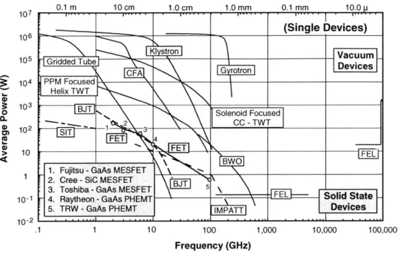
1-1 Recent advances in vacuum electron device technology showing
gyro-devices pushing the frontier to higher power and higher frequency. . . 19
1-2 Common gyro-device cavity profiles with an electron beam: (a)
gy-rotron oscillator; (b) gyro-TWT; (c) gyroklystron. . . . . 21
2-1 The current DNP test bed utilizes a, 140 GHz gyrotron, waveguide with
2 miter bends and a downtaper, a DNP probe, and another
supercon-ducting magnet. Losses were measured previously. . . . . 28
2-2 The system block diagram: (1) Electron gun (MIG), (2) Solid state RF
source, (3) Superconducting magnet, (4) Cavity circuit (gyroklystron
shown) and (5) Mode converter. . . . . 29
2-3 The predicted magnetic field profile shown at the rated maximum field
strength of 6.2 T. The ±0.5% uniform field length is 28 cm and the field falls off as roughly B, ~ 1/z 4 in the vicinity of the cathode, which
is located at z = -55 cm . . . . . 32
3-1 Diagram of beam cross-section showing the guiding center and Larmor
rad ii. . . . . 34
3-2 Diagram of the typical triode MIG showing the beam and two anodes. 35
3-3 Diagram showing the definitions in a simplified system of conical
elec-trodes... ... 37 11
3-4 Evolution of electrons in phase space: (a) Initial uniform distribution of phases; (b) acceleration of electrons; (c-d) formation of the bunch and transfer of electron momentum; (e-f) spent beam. (Courtesy of J.
A nderson) . . . . 43
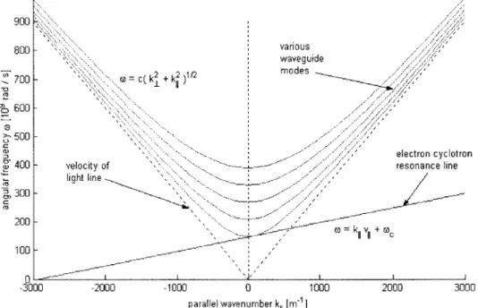
3-5 Uncoupled dispersion diagram for waveguide modes and resonance line. 49
3-6 Plot of the oscillation start current versus B-field strength for various
modes in a cavity designed to support the TE02 mode. ... 52
3-7 Efficiency contours of an optimized gyroklystron. (a) Optimized
per-pendicular efficiency
rL.
(b) Bunching parameter q. (c) Detuningparameter A. (d) Relative phase 0. . . . . 54
3-8 A sample output from a non-linear, non-stationary imacroparticle code
showing the temporal evolution of the fields in the cavity (Courtesy of
J. R . Sirigiri). . . . . 55
3-9 The mode conversion process: A circumferentially perturbed pipe
con-verts TE02 to TEO; A "snake" converter transforms TEO to TE,
and a scalar horn followed by overmoded corrugated waveguide
con-verts TE1 1 to H E ,. . . . . 57
4-1 Profile of a 5-cavity gyroklystron with a linear uptaper section (top),
Evolution of electric fields in the cavities (bottom). . . . . 62
4-2 Two methods for lowering the cavity total
Q:
(a) loading the cavitieswith lossy ceramic inserts to lower the ohmic
Q,
(b) lowering diffractiveQ
by leaky slots. . . . . 664-3 An HFSS simulation of a PBG structure to confine the TE02 mode.
(Courtesy of J. R . Sirigiri) . . . . 66
4-4 Output from an independent code based on linear theory showing
tar-get unsaturated gain of around 40 dB obtained with 5 cavities and
cavity field amplitude F = 0.04. . . . . 68
4-5 (a) Characteristic power saturation and over-saturation; (b) optimal saturated electron bunching and (c) over-bunching due to an elongated
structure. . . . . 72
4-6 The effect of velocity spread on an amplifier system. The power
in-creases up to a point and the peak shifts to higher frequencies due to the slower electrons. Note that the bandwidth at the 50-watt level
around 140.8 GHz is increasing with increasing velocity spread. . . 77
4-7 Current variations on the final design. The design value of current is
10=0.15 A, showing a -3 dB bandwidth of 1050 MHz, a bandwidth of 1270 MHz at the 50 Watt level, and a peak power of 130 W. ... 80
4-8 Magnetic field variations on the final design. The design value is
BO=51.38 kG. Even over a BO deviation of 0.4%, over 1 GHz of BW is
available at 50 W . . . . 81
4-9 Input power variations: The design value is P,=25 mW. . . . . 82
4-10 Gain and output power versus input power. The linear gain is 39 dB and the saturated gain is 36 dB. The frequency here was 140.5 GHz,
roughly the peak of the power spectrum. . . . . 83
4-11 Velocity spread variations. The design value was 4%, but it delivers
over 1 GHz of BW at 50 W even with 6% spread. . . . . 84
4-12 Beam pitch factor (a) variations. The nominal value is 1.5 for the design. 85
4-13 The electric field profiles in the cavities for several frequencies. .... 86
4-14 The pulse shapes for a 4 ns trapezoidal pulse showing a propagation
delay of approximately 1 ns. . . . . 87
4-15 The preliminary work on the input coupler (quarter-slice shown): (a)
139.4 GHz; (b) 140.0 GHz; (c) 140.3 GHz. . . . . 89
5-1 The MIG parts: Cathode, Anode 1, Anode 2 ("mod-anode"), shown
with an electron beam and the equipotential contours. . . . . 92
5-2 The EGUN simulation results for the 20 kV MIG design (Courtesy of
J. R . Sirigiri). . . . . 94
5-3 The dimensions in millimeters of the gun section used for the EGUN
sim ulation. . . . . 95
6-1 The gyroklystron output section consisting of linear and nonlinear
up-taper sections. . . . . 98
6-2 The results of the simple equations and the CASCADE simulations
show reasonable agreement. The mode converter consists of N = 5
periods and has a bandwidth of 14 GHz and a peak efficiency of 98.6%. 99
7-1 The preliminary design of a 500 W gyroklystron circuit with a 27 kV,
0.4 A electron beam and saturated gain of 47.4 dB at 6% transverse
velocity spread. . . . . 103
List of Tables
1.1 Gyroklystron Achievements
3.1 Key MIG design parameters
4.1 4.2 4.3 4.4 4.5
Coupling Coefficient Cyp for Initial Design Parameters. First Design Parameters . Second Design Parameters Final Design Parameters .
TEop modes
5.1 MIG Design Parameters . . . . 7.1 500 W GKL Preliminary Design Parameters .
15 24 36 64 71 74 76 79 93 104
Chapter 1
Introduction
The gyroklystron amplifier is a high frequency vacuum electron device (VED) used to amplify electromagnetic waves with wavelengths on the millimeter scale to higher power levels. The gyroklystron is part of a larger class of general fast wave gyro-devices that utilize the electron cyclotron resonance maser (CRM) instability. The possibility of an electron beam interacting with an electromagnetic wave was known
by the end of the 1950s, laying the foundation for all gyro-devices [1]. In particular, the gyrotron oscillator research that has been going on since the 1970s has focused primarily on applications for plasma heating in the millimeter band range of 28 GHz
to 170 GHz, at power levels typically greater than hundreds of kilowatts or more
[2].
More recently, gyrotron amplifier research has begun to take root in fertile fields such
as radar
[3],
target tracking, imaging, cloud physics [4] [5] and experiments utilizingDynamic Nuclear Polarization (DNP) [6] [7].
In gyro-devices, a weakly relativistic electron beam gives up energy to radio fre-quency (RF) electromagnetic fields in the cavities through bremsstrahlung, a process whereby the electrons emit radiation as they experience forces from the electromag-netic fields. The term fast wave comes about because the phase velocity of the electromagnetic wave in the interaction structure is faster than the speed of light. In this regime, the cavity structures are typically several wavelengths long and the energy is extracted from the perpendicular component of the electron momentum. In contrast, the interaction structure of the slow wave device keeps the RF phase
ity below the speed of light so that the electrons travel in synchronism with the RF fields. When this happens, Cherenkov radiation is emitted by interaction with the parallel component of the electron's velocity instead of the perpendicular component. In both slow wave and fast wave devices, the transverse dimensions of the interaction structure scale inversely with frequency, which limits the power that can be safely generated in the structure due to the increased ohmic losses. Fast wave devices can, however, operate in higher order modes very efficiently. This allows the dimensions of the interaction structures to be larger, making it possible to generate higher power while limiting the thermal losses in the structure. The efficiency of slow wave devices is very poor at higher order modes and thus the fast wave devices have a distinct edge at the millimeter wave frequencies and above.
The gyroklystron amplifies RF via a focused electron beam travelling through a series of resonant cavities. It is the fast wave extension of the klystron, which is itself a slow wave device used for generating microwaves. Gyroklystrons are known for their high efficiency and ability to provide high power in a frequency band that is out of reach for both slow wave and laser devices (Fig. 1-1) [8]. Among the competitors for the microwave band are conventional microwave tubes such as klystrons, magnetrons, travelling wave tubes (TWTs), backward-wave oscillators (BWOs) and other slow-wave devices. In the millimeter band, the competition thins out, leaving gyro-devices as the only practical high-power sources. BWOs, Orotrons, and even some solid state devices are capable of producing power in the millimeter bands, but do not extend to sub-millimeter wavelengths at the necessary power levels. By operating at integer harmonics of the fundamental, gyrotron devices have achieved operation frequencies of up to 889 GHz [9].
1.1
Motivations for the Gyroklystron
Since this gyroklystron will be incorporated into an existing DNP experiment at the Francis Bitter Magnet Laboratory, Cambridge Massachusetts, it is a desirable feature that the source be capable of continuous wave (CW) operation as well as
0 CC L. (D 107 106 105 104 103 10 10 10-1 10-2 .1 10 100 Frequency (GHz) 1,000 10,000 100,000
Figure 1-1: Recent advances in vacuum electron device technology showing gyro-devices pushing the frontier to higher power and higher frequency.
scale short pulses. The short-pulse capability requires a fairly wide bandwidth and a high amount of phase stability. The CW operation is much easier to achieve at low electron beam power, whereas an amplifier would lend itself to phase-stable short pulses [10]. Furthermore, lab safety is an important consideration, as higher voltage makes shielding the power wires considerably more challenging. Unfortunately, the lowering of beam voltage in most amplifier devices causes the bandwidth to become narrow, but the gyroklystron provides a series of cavities that can be tuned to differ-ent resonant frequencies to widen the bandwidth at the expense of amplifier gain, a method known as stagger tuning [11]. The cluster cavity [12] technique can theoreti-cally widen the bandwidth without losing gain if the cavities are uncoupled, but this has yet to be achieved in practice. Another challenge of low beam power is that the gain is severely restricted at low beam currents.
(Single Devices)
Vacuum
Gridded Tube
lDevices
.PPM Focuede
Helix TWT
Solenoid Focused
\2 CC - TWT
FETE4
1. Fujitsu - GaAs MESFET\
2. Cree - SiC MESFET'
3. Toshiba -GaAs MESFE T T 5
4. Raytheon - GaAs PHEMT Folid State
5. TRW -GaAs PHEMT IMPATT Devices
0.1 M 10 CM 1.0 crm 1.0 MM 0.1 MrM 10.0 LI
1.2
Description of Operation
In all gyro-devices, an electron beam is emitted from an indirectly heated cathode and guided along a precision magnetic field through a single cavity, series of cavities, or a long gyro-travelling wave tube (gyro-TWT) section. The electron beam consists of many electrons gyrating around the magnetic field lines in a. small helix with a, cyclotron frequency near the operating frequency of the device as they propagate from the cathode side of the tube to the collector side. These small helicies form a, larger hollow annular ring beam.
If the Larmor orbits of the electrons are smaller than the guiding center radius
(average radius of the hollow annulus), then the device is called a small orbit device. On the other hand, if the Larmor radius is greater than or equal to the guiding center radius, the device is said to be a large orbit device. A small orbit beam can be easily generated by a Magnetron Injection Gun (MIG), and this is the type of beam we will utilize here. The generation of a large orbit beam is more complicated and is usually achieved by imparting a kick to a linear beam by either a magnetic cusp or a, microwave kicker.
Energy is extracted in the gyrotron interaction by the relativistic cyclotron res-onance maser instability in which the electrons are phase bunched in the azimuthal direction due the RF fields. The bunches grow along the beam, and if the operating frequency is slightly higher than the cyclotron frequency of the electrons, the bunches
end up in the decelerating phase of the microwave field and give up it energy to it
f13].
Only the transverse energy is extracted from the electron beam during a CRM fast wave interaction and hence an electron beam with significant transverse energy is
chosen in a gyrotron device. Typically the pitch factor, or the ratio of the transverse
energy to the longitudinal energy of a gyrotron beam varies from 0.5 to 2.0 and is given the symbol a.
At the end of the interaction, the beam has lost a significant amount of its original energy to the RF fields in the cavities and is collected by a thermally cooled collector. The remaining RF fields are extracted from the tube and sent through waveguides to
electron
beam
(a)
Pin
Pout
.- j1.
1
L-.
()---
---
-- -
-
--- -
--- - -- --- -- --
----Pin
Pout(C)
Figure 1-2: Common gyro-device cavity profiles with an electron beam: (a) gyrotron oscillator; (b) gyro-TWT; (c) gyroklystron.
the desired application. The particular variation of the interaction circuit falls into several categories [14]:
1.2.1
Gyrotron
The gyrotron oscillator consists of a short cylindrical resonant cavity section bounded on either side by a down-taper and up-taper (Fig. 1-2a). The energy is extracted from the uptaper section and often sent through an internal quasi-optical mode converter in high power gyrotrons. High power gyrotrons usually operate in a high order mode,
such as the TE22,6 mode so that a larger electron beam diameter can be used to
reduce the problem of space charge [15]. A mode converter is necessary to change this mode to a Gaussian-like mode to further reduce spurious mode conversion and transmission loss through a waveguide transmission line.
1.2.2
Gyro-TWT
Gyro-TWTs are capable of very high gain and large bandwidth due to a near match-ing of the waveguide mode and cyclotron mode and because the group velocity is very close to the electron beam velocity. The interaction structure is most simply a waveg-uide with no resonant structures, so the bandwidth can be quite large (Fig. 1-2b). Velocity spread is typically the limiting factor for how long a structure can be. The gyro-TWT often suffers from problems with instabilities and self-oscillation due to spurious backward waves, although the more recent use of heavily- loaded, lossy TWT waveguides was found to be a good way of controlling these problems. Gyro-TWTs have not been built at very low beam voltages.
Another version of the gyro-TWT uses confocal waveguide to avoid the use of expensive, fragile and often temperature-sensitive lossy ceramic materials. The con-focal gyro-TWT was first successfully demonstrated at MIT [16]. The large gap on
either side of the waveguide lowers the total
Q
by diffraction, allowing it to be easilybuilt without the use of lossy ceramics. In a confocal waveguide, the diffractive losses from the open sidewalls allow the suppression of lower-order modes. Thus, using it in a gyro-TWT allows operation in higher-order modes without mode competition. This in turn allows the the use of an interaction structure with larger transverse di-mensions and hence higher power handling capability. Because part of the annular electron beam sees no RF fields, efficiency is lower than the gyro-TWT. Mode con-version may also be more difficult from the hybrid modes to lower-order Gaussian beams.
The new possibility exists of building a gyro-TWT using Photonic Band Gap (PBG) structures. The PBG gyro-TWT would consist of a 2-D lattice of rods peri-odically spaced with a defect in the lattice where some rods are removed. The PBG interaction structure can be designed so that the backward wave frequency lies in the passband of the PBG structure and hence leaks out of the lattice. This is likely
to dramatically reduce the
Q
of the structure for the backward wave mode andal-low operation at higher beam currents in the forward wave amplifying mode. Hence 22
the result is a mode-selective structure supporting only the design mode. A PBG gyrotron oscillator was demonstrated at MIT [17]. A PBG amplifier has yet to be built.
1.2.3
Gyroklystron
A gyroklystron consists of a series of nearly isolated prebuncher cavities, each of
which bunches the electrons such that gain occurs in each cavity (Fig. 1-2c). In theory, the gyroklystron can have as much as 18 dB of power gain per cavity in the linear regime [18], lending gyroklystron devices to relatively short circuits. A small RF signal is coupled into the first cavity, then amplified in each cavity and finally extracted at the end. Gyroklystrons typically have very good linearity, less sensitivity to velocity spread and can have considerably wide bandwidth even at low beam voltages. Since the gyroklystron typically has a more narrow bandwidth than the gyro-TWT, it is also less noisy. This device, however, is more difficult to build, since several cavities have to be tuned properly and the alignment of the cavities with the electron beam can be difficult. Furthermore, the drift spaces, where ideally no fields exist, are susceptible to a plethora of modes and resonances in practice.
A common method for adjusting the
Q
factor of each cavity in the gyroklystron is to use lossy ceramics. However, other possibilities exist, such as lossy tunable slotsin the cavity that would lower the
Q
by diffracting some power out. Large slots couldbe used in the drift sections to allow the fields to leak out and be absorbed by larger lossy ceramics.
1.2.4
Gyrotwystron
A gyrotwystron is a hybrid device consisting of a gyroklystron section followed by
a gyro-TWT section. Utilizing this configuration rather than a plain gyroklystron alone, higher bandwidth can be achieved, as well as extra protection against RF breakdown. Another version is the inverted gyrotwystron, where the travelling wave section appears first. The gyrotwystron is typically more susceptible to oscillations
Table 1.1: Gyroklystron Achievements
Source V [kv] Io [A] POt [kW] eff fo [GHzI BW [MHz] gain [dB] CPI, NRL [19] 55 6.0 10.2 (ave) 31% 95 700 (0.74%) 33 NRL [20] 72 9.6 208 (pk) 30% 35 178 (0.51%) 53 CPI, NRL [21] 53.7 5.1 72 (pk) 27% 95 410 (0.43%) 50 CPI, NRL [21] 56 4.4 84 (pk) 33.8% 95 370 (0.39%) 40 CPI, NRL [22] 58 4.2 60 (pk) 25% 93 640 (0.68%) 27 CPI, N1RL [23] 65 6 80 (pk) 29.5% 94 600 (0.64%) 24.7 Nusinovich [24] 40 0.3 1.0 (pk) 8.5% 360 72 (0.02%) Proposed GKL at MIT 15 0.15 0.10 (cw) 5% 140 1000 (0.71%) 36
than the gyroklystron. sparse.
Not many have been built and the documentation is rather
1.2.5
Gyro-BWO
In a BWO, the output frequency is directly adjusted by the operation voltage, but higher magnetic fields are required for the BWO than for other gyro-devices because of a negative Doppler shift, making the BWO undesirable at very high frequencies. BWOs also suffer from a relatively low efficiency and low output power.
1.3
Previous Gyroklystron Work
Many advances have been made recently in the field of gyroklystron research. Tab. 1.1 lists several examples of gyroklystrons that have been built recently.
Some gyroklystron design advances and variations include a dual-cavity coax-ial gyroklystron [25], third-harmonic gyroklystrons [26], and sub-millimeter second-harmonic designs [24]. In addition, many advances have been made in the theory of gyroklystrons, such as the optimization of gyroklystron efficiency [181, AC space
charge analysis [27], the effects of penultimate cavity position and tuning [28], and
the theory of stagger tuning [29].
1.3.1
Novel Features of this Design
Because it is desirable to have CW operation on the order 100 W, a low beam power is necessary to maintain reasonable efficiency. A low beam voltage would lend itself to lab safety. Thus one aspect of this design that is considered novel is low beam power. Operation as such low voltage (leading to a more weakly relativistic beam) and low current poses significant challenges. Low voltage causes the bandwidth to become more narrow as the cyclotron resonance line intersects the waveguide modes near cutoff and also makes it difficult to avoid problems with space charge. Low current significantly reduces the gain. Most gyroklystron designs have operated in the neighborhood of 60 kV and above 4 A, whereas this design focuses on 15 kV at
0.15 A. No gyroklystron has ever been designed with such a low beam current.
The use of Photonic bandgap (PBG) resonators has been evaluated to reduce or eliminate mode competition in the cavity circuit as well as a novel method for
adjusting the
Q
in the cavity without use of lossy dielectrics or ceramics.1.4
Thesis Outline
Chapter two is an overview of the whole design, chapter three summarizes the theory behind the operation of gyroklystrons, chapter four focuses on the cavity circuit, chapter five shows the details of the electron gun design, chapter six touches on the nonlinear uptaper and mode converter and chapter seven is the conclusion.
Chapter 2
Overview of Program
Here is presented an overview of the whole test bed already in place at the Francis Bitter Magnet Lab (FBML) in Cambridge, MA, as well as an overview of the proposed gyroklystron amplifier.
2.1
Overview of the Current Experimental Setup
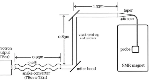
The current Dynamic Nuclear Polarization enhanced Nuclear Magnetic Resonance (DNP/NMR) test bed at the FBML consists of a 140 GHz gyrotron, waveguides, a
DNP probe and another superconducting magnet (Fig. 2-1). The gyrotron delivers
approximately 15 Watts in the TEO, mode into a snake mode converter which
trans-forms it to the TE11 mode before it propagates down straight copper pipes. Two
90' miter bends exist before the oversized waveguide is tapered down to fundamental
waveguide. The total losses were measured previously to be approximately 6.4 dB with theoretical losses totalling 3.7dB [30]. At the probe, approximately 1 to 2 watts
of power is delivered into the sample.
In this DNP test bed, the 140 GHz gyrotron will be replaced with the proposed 140 GHz amplifier. The amplifier will deliver approximately 100 Watts in the TEO, mode into the existing snake converter. If the existing waveguide is also used, the resulting power at the probe is expected to be in the tens of Watts. A newer
sys-tem including a TE1 1 to HE,, scalar horn mode converter and low-loss corrugated
gyrotron output (TE0i) 0.93m -0..5(IB J snake converter (TEoi to TE11) 1.33M> taper -4dB taper -2-5dB total wg
o.83m and mirrors
probe J
miter bend miter ~, bed_______ NMR magnet
-Figure 2-1: The current DNP test bed utilizes a 140 GHz gyrotron, waveguide with 2 miter bends and a downtaper, a DNP probe, and another superconducting magnet. Losses were measured previously.
waveguide lines are also available to lower the spurious mode conversion and waveg-uide losses, if needed. The amplifier will feature ease of frequency tunability where previously only a single frequency was used, and it will also allow nanosecond-scale short pulses to be sent to the samples.
2.2
Overview of the Gyroklystron Operation
Referring to the block diagram of the gyroklystron in Fig. 2-2, an indirectly heated cathode ring in the electron gun at one extreme of the gyroklystron tube emits an annular beam of electrons by thermionic emission in a carefully designed region with high electric fields. The electrons adiabatically spiral around the magnetic field lines created by the magnet. The size of this spiral is determined by the Larmor radius which is related to the static magnetic field and the relativistic mass of the electrons. The electrons are initially randomly distributed in phase over the range (0, 27r) and are assumed to produce a uniform current density over the area of the annular ring.
The gyroklystron cavity circuit consists of an alternating series of cavities and drift spaces. In the first cavity, RF power is coupled in from an external source. As
* Source 140 GHZ RF Gunn & IMPATT To Experiment Electic Field Profile 1OOW RF RH~
0Cavity
CircuitGin Coil
*
Mode Convertero
Electron Gun0
6.2T MagnetFigure 2-2: The system block diagram: (1) Electron gun (MIG), (2) Solid state RF
source, (3) Superconducting magnet, (4) Cavity circuit (gyroklystron shown) and (5) Mode converter.
the electron beam enters the first cavity, the electric field produces a force on the electrons as they spiral around the magnetic field lines. This force not only changes the phase of the electrons as their orbits are slowed down and sped up, but it also causes the electrons to emit bremsstrahlung radiation, which is superimposed over the existing fields in the cavity. This effect of changing the perpendicular momentum of the electrons by interaction with an electric field leads to a process called bunching, which causes a majority of the electrons to emit bremsstrahlung in phase coherently. After the first cavity, the electron beam enters a cutoff region called the drift space where the electromagnetic fields cannot propagate (evanescence). The electron phases, being affected by the RF-induced forces in the first cavity, continue to evolve in the drift space in a process known as ballistic bunching. The purpose of the drift space is two-fold: To isolate adjacent cavities from coupling to one another, and to allow the bunching to evolve. A beam that is more highly bunched tends to emit bremsstrahlung in phase and hence emits more RF energy. However, if the beam
is allowed to evolve too long, or if the bunching process is forced too strongly, an overbunching may result in which the efficiency drops dramatically. Longer drift spaces then have the effect of increasing the gain, unless they are too long.
Upon entering the second cavity, where no pre-existing RF is present, the electrons give off RF at the Doppler-shifted frequency given by the beam line relation. If the cavity is tuned properly, the bunching in the beam will be reinforced and the total RF fields in the second cavity will be higher than those in the first cavity. The second drift space has the same function as the first. This process continues in each following cavity up to the fifth cavity in this design.
In the last (fifth) cavity, the RF energy is extracted from the beam, allowed to
travel through the uptaper section and then converted from the TE02 mode to a more
versatile Gaussian-like mode, such as the HE,, mode using a mode converter. The mode conversion process happens in three steps. The Gaussian-like modes propagate through the corrugated transmission lines and windows with very low loss and low mode conversion compared to the TEr,, schemes [31].
The extraction cavity and uptaper must be very carefully designed to prevent mode conversion from the design mode to unwanted modes. Usually, a nonlinear uptaper is used to achieve this. Furthermore, this nonlinear taper must not allow RF oscillations to occur from the spent electron beam.
Finally, the spent electron beam will be collected in the collector region, where the beam dissipates on a water-cooled wall. The RF will reach the mode converter and then propagate through an oversized, low-loss corrugated waveguide to the ap-plication.
2.2.1
The RF Source
The low-power RF source must be able to supply approximately 50 mW CW with a bandwidth of greater than 1 GHz at a center frequency of 140 GHz. The source should also be capable of generating short pulses and be very phase stable. Possible systems include an IMPATT diode injection locked by a GUNN diode in a 4-phase pulse-forming network.
2.2.2
Superconducting Magnet
The high precision superconducting magnet for this experiment was requisitioned from Magnex Scientific, LLC. The maximum field strength is 6.2 T with a ±0.5% uniform length of 28 cm. The magnet has a 5-inch horizontal, room-temperature bore with a, flange at one end for mounting the external, copper gun coil. A unique feature of this magnet is that it is actively shielded such that the magnetic field falls
off as Bz ~ i/z- in the vicinity of the cathode. Fig. 2-3 shows the predicted magnetic
field profile along with the fall-off exponent of the field strength.
2.2.3
Power Supply
The power supply must be capable of supplying at least 15 kV at 0.15 A continuously and should be capable of millisecond-scale pulses. It may be necessary to have a power supply capable of microsecond-scale pulses. Furthermore, the unit should be capable of interfacing with a computer to facilitate automation and data acquisition.
2.3
Main Components
In the following chapters, the electron gun, cavity circuit and mode converter will be discussed in detail. These are the main components that require careful design in this project.
Magnetic Field Profile
-60 -40 -20 0 z-distance [cm]
20 40 60
The predicted magnetic field profile shown at the rated maximum field
6.2 T. The ±0.5% uniform field length is 28 cm and the field falls off as
~1/z4 in the vicinity of the cathode, which is located at z = -55 cm.
32 B ~ 1/zn +/-0.5% uniform length: 28cm -z B n 7 6 5 0 4 0 E2 0 Figure 2-3: strength of roughly Bz 80 -1L_ -0
Chapter 3
Theory
In the first section of this chapter, first-order design equations are presented for elec-tron gun design. The first-order design is an essential part of optimizing an elecelec-tron gun. Next, the electron cyclotron interaction is explained and the gyroklystron theory is presented in its linear and non-linear forms. Lastly, the topic of mode conversion is discussed.
3.1
Magnetron Injection Gun
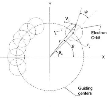
The Magnetron Injection Gun (MIG) is responsible for generating the high quality electron beam necessary for successful operation of the gyroklystron. Figure 3-1 shows a cross sectional slice of the electron beam and the typical electron orbit. Since the electrons do not cross the straight, axial magnetic field lines, 00 and r. are essentially fixed for a given electron in a constant magnetic field. This means the current density is approximately constant throughout the length of homogeneity in the magnetic field. The Larmor radius along with other parameters used in this section are defined below in Sec. 3.1.2.
The characteristics of the electron beam are determined largely by the operation voltage, V, which controls the acceleration, and therefore the velocity, of the electrons as they are thermionically emitted from the cathode. The relativistic constant -,0
Y 'N V r
A
Electron Orbit rg Guiding centers AFigure 3-1: Diagram of beam cross-section showing the guiding center and Larmor radii.
relates V to the velocity components of the electron, vi and vIl as
Vo(kV)
511
where m, is the electron mass and c is the speed of light. For a typical design voltage
of around 60
kV,
-yo ~ 1.12. The values for v1 and vIl are obtained by using thedefinition of the pitch factor:
o
= vi/vll. The magnetic field controls the frequencyat which the electrons orbit the magnetic field lines through the relativistic electron-cyclotron equation:
=eB
_-
V(3.2)Yome TL
where e is the charge of an electron and rL is the Larmor radius at which the electron orbits around the magnetic field.
MIG designs are typically either diodes or triodes. In the triode configuration,
there are two anodes (Fig. 3-2). The first anode is responsible for accelerating the 34
(3.1)
-V
2 -1/2
-B RF interaction region B-field
B Cath. field
BC
Axial
B-field profile
Second
Anode
X Firstd 11 RF interaction L region LngthC Ring Electron beam
Cathodn
Gun axis
Figure 3-2: Diagram of the typical triode MIG showing the beam and two anodes.
electrons up to the desired relativistic level, while the second anode allows the user to tune parameters such as the pitch factor, a. In a diode configuration, the potentials on both anodes are the same and they are fabricated as one unit. The advantages of the diode configuration are that the power supply is much simpler and that there are fewer ceramic insulation rings, which can be a source of electrical breakdown problems and also drive up the cost and complexity. With a diode there also are fewer parameters to optimize in the experiment. In the case where tuning a is important, or where the electron beam requirements are such that the diode design does not meet the specifications well, then a triode structure must be used.
In MIG design, there are five primary parameters constrained by the require-ments of the system and four free variables that must be optimized for any given set of primary parameters [32]. These parameters are listed in Tab. 3.1. Additional con-siderations beyond these nine key gun design parameters are the mode of operation in the tube, harmonic number, and magnetic field requirements or constraints.
Table 3.1: Key MIG design parameters
Parameter Symbol Design value
Beam power P = V x J" 2.3 kW
Electron energy YO 1.029
Cyclotron frequency
we
2-F x 140 x 109 rad/sGuiding center radius rgo 0.64 mm
Pitch factor a ='v±/vil 1.5
Cathode Radius rc 4.02 mm
Cathode Current Density Je 2 A/cm2
Cathode Slope Angle
#c
500Cathode-Anode Spacing Factor DF 3
While computer codes are very important in optimizing the electron gun design, it is important to start with a, good first-order design. Typically, the most important parameter is the cathode radius, r,. For some choices of variables, such as low voltages (corresponding to low -yo), no suitable r, exists due the presence of space charge.
Analysis for a first-order cavity design begins with the assumptions of cylindrically symmetric DC fields in the cavity, E(r,z) and B(r,z), as well as an assumption of conservation of momentum. To lowest order, B(r,z) can be assumed to be constant over the thickness of the electron beam, and thus becomes simply B(z), where the boldface indicates a vector quantity.
The following first order analysis for the MIG is presented in Baird, et al [32]. The fundamentals of MIG design are cast in a way that simplifies the design down to the four free variables that were listed in Tab. 3.1. The definitions for the parameters used in this section are defined below in Sec. 3.1.2.
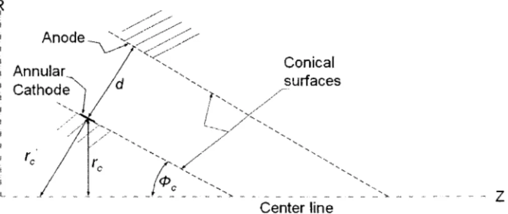
Figure 3-3 shows the first order approximation of the electron gun as two con-centric cones. The DC electric fields in this configuration are approximated by the equation for potential in a cylinder using a substitution to obtain the cones:
E (r) = V " (3.3)
I n( r' /r')
where r' co) and r' =r + d.
The spacing factor, DF, is normally
chosen
to have a minimum limit of 2, whereAnode Annular Cathode d rc rc I -, L( Conical surfaces Center line
Figure 3-3: Diagram showing the definitions in a simplified system of conical elec-trodes.
the beam clears the anode wall by one Larmor diameter. DF satisfies the following
equation as a function of guiding center radius rg, and Larmor radius, rL,
DF = d o _L Cos c (3.4)
TLrgo
Larger values of DF give more clearance and also require higher second anode voltage.
At the point where the first and second anode voltages are the same, the second anode becomes unnecessary.
The magnetic compression ratio, Fm, can be written,
Bo
F- = = 2RC (3.5)
The normalized slant length, L,, and the normalized cathode radius, R,, are
related by,
L,
Re
10 1
27r 2Je R2 (3.6)
The ratio of guiding center spread to guiding center is given by,
SR
9 sin OcR
9 K~2±+1 I0 1 27rr%2Jc R2 37Z
(3.7)The cathode to anode spacing variables, Dac and DF are related to the cathode angle,
Dac _ DFK (3.8)38
Re cos Oc
The normalized potential is given by,
ln(1
+
DFr)4
-y
2 - CV 1 + 23.(Da = F + -_ 1 (3.9)
" ln(1 + 2r,) K2 R2 COS2 Oc a2 + I I + 2K
The electric field should never exceed approximately 100 kV/cm to prevent arcing, although the actual design may need to be much below this limit. The cathode nose is typically a point of high stress. One way to alleviate high electric field gradients is to increase the cathode radius, r,. The possibility of arcing places a, lower limit on
rc-Ec _ moc2/e E, 4)aCOS Da -Tnoc2 cos
#c
C / _11(3.10) Emax EmarrLo in(1 + DFK) RcThe ratio of beam current density to Langmuir limiting current density, Jc/JL, must be kept below 15-20% because adiabatic MIG design assumes negligible effects of space charge. As rc is increased, this ratio quickly increases, and this equation sets a hard upper bound on the size of r, since it scales as approximately ri:
_c -=- 27rri 2Jc(1 + DFK)C2 R2
- - (3.11a)
JL 4.0 X 0-6gC2/e3/2 COS2 Oc <3/2
AL 14.66 x 10⁻⁶(mrno)/co2 b (Da 3.1a
1 + _ 5 24
1
C1 exp(-C 2/2)
[C
2 + -0C2 + 300 + 9900 C (3.11b)C2 ln(1 + DFK) (3.11c)
where Eq. 3.11c is accurate to three significant figures up to C2 3.0. If one finds the
lower bound on rc from (3.10) is greater than the upper bound from (3.11), then that MIG design might not be possible unless beam voltage is increased or ao is lowered. The perpendicular velocity, can be approximated as follows for small cylindricity parameter, K:
F3/2 Ec cos (1
UvLo ~ o, (3.12)
where the following relation also holds:
A- aV 2 (3.13)
VII V1
The assumption of adiabatic flow, meaning that the perpendicular energy of the electrons is proportional to B(z), can be violated if the variations in the static electric or magnetic fields occur on a scale smaller than the gyro-orbit of the electron:
d {BE}
-{B, E} < ' (3.14a)
dz ZL
d2 {B E}
dz2{B, E} < 'ZL, (3.14b)
where ZL is the axial length travelled by the electron during one cyclotron orbit. In the vicinity of the cathode, care must be taken to form shapes that promote adiabatic flow. An elongated cathode nose is occasionally used to produce quick variations in E-field, but this can lead to large non-adiabatic effects.
3.1.1
Other Sources of Velocity Spread
Besides the velocity spread due to geometric optics, velocity spreads also occur due to thermal non-uniformity and roughness of the cathode surface. Estimates of these
values are given by Tsimring
[33]:
A V_ KTc Fm 1/2 1 (3.15)
VI T [n 0 y,
I
v1 0A vi 0 4 2eEcR Fm1 /2 1 (3.16)
V" ) R m0 70 V 0
where K is Boltzmann's constant, T, is the cathode temperature in Kelvin, and R is the radius of a small hemispherical bump characteristic of the cathode roughness. The spreads are estimates of the standard deviations of the velocities such that the
average spread width would be given by ±(Avi/vi).
These spreads due to optical, thermal and roughness effects combine orthogonally,
(Aj UI
j
0
0
Ui) + (A[(A2 2 (AV)2- 1/2
\E- / total \ L / 0 \0- / T \ -L /_ (317
Generally, one can expect the total spread to be at least double that of the optical spread when the roughness and thermal spreads are included. The value of total perpendicular spread assumed for this design was 4% (parallel spread of 9%).
3.1.2
Variable Definitions for MIG design section
Vo = Beam voltage, volts
I0 = Beam current, amps
0 =1 + eVo/moc2 1 + V(kV)/511 = relativistic mass factor
VO = c(1 - 1/7 )1/2 - electron velocity, M/s
vZO = vO/(a + 1)1/2 - longitudinal velocity, m/s
ao = V-Lolvzo = pitch factor
L,, = 2,rfcO = eBo/mo'o =relativistic cyclotron frequency, rad/s
rqo = guiding center radius at RF interaction region, in rLo vi/o'c = Larmor radius at RF interaction region, m
R9 = rgo/rLo = normalized mean guiding center radius
6Rg = 6rgo/TrLo = normalized full width guiding center spread
= (R 2 _ 1)-1/2 = cylindricity parameter
Fm = Bo/Bze = magnetic field compression ratio R = rc/rLo = normalized mean cathode radius
Oc = Cathode tilt angle (always positive)
LS = 1l/rLo = normalized slant length of cathode
DF = Cathode to Anode spacing factor (select DF > 2)
Dac = d/rLo = normalized slant spacing between cathode and anode (D a = eVa/moC2 = normalized first anode voltage
Ec = Cathode electric field
Emax ~ V/m as a conservative value
Je
= Temperature limited cathode current density, A/rM2JL
= Langmuir space charge limited current density, A/n 23.1.3
Computer Codes for MIG design
If Jc/JL in Equation (3.11) seems questionably high, the self consistent MIG design
codes will indicate whether there is a space charge problem or not. These codes typically do not, however, estimate the spread due to thermal non-uniformity or surface roughness, which must be considered separately.
Currently, there are several common MIG design codes available, such as several versions of EGUN [34], OMNITRACK (2D and 3D) [35][36], and MICHELLE [37].
EGUN was used extensively in the design of this MIG. These computer codes
self-consistently compute the trajectories of the electrons as they propagate from the cathode down through the cavity region. In the problem of the moving charge, it is important to consider the self-consistent effects. Since the electron is a charge, it experiences forces from the electrostatic fields in its path and simultaneously alters them. Since it is also a moving charge, it generates a current of its own and therefore a magnetic field, which affects the total magnetic field it experiences. 2-D codes have been able to handle this just fine for over 20 years, but the newer 3-D codes require a lot of computer power to get a fine enough mesh and time resolution for the simulations. 3-D gun codes are gaining popularity in the multi-beam klystron (MKB) community, where it is very important to consider everything in the full three dimensions. 2-D gun codes are usually sufficient for present day gyro-devices, but
3-D codes can be used where it is desirable to simulate the effects of, for example,
non-uniform cathode emission.
3.2
The Cyclotron Resonance Maser interaction
Once the electron beam has been generated, it is passed through a series of cavities where it interacts with RF fields in the cavities. In this section, we will consider the RF fields in the cavities and the phase space of the electrons (since we already determined that their position averaged over orbit is essentially fixed). Let us again
0.3
E aRL
-. S a S S S S S S-0.3 t=05
-0.3
0.3--0.3
S a a S S S S S * Ux (mm)
a.
E
180 Ps
x(mm)
C.
0.3
a 0 S 0 S a0.3
0.3
-0.3 t
-0.3
0.3
-0.3
t
-0.3
.,..aeeaa... a RL *0.. * S * a * a * 0 9 a * S a S a S S90 Ps
x (mm)
b.
E
0 a 0 a %=pS S U S270 ps
x (mm)
d.
E-)
'R*
t
=360 ps
.3
x (mm)
e.
a0.3
0.3
-0.3 t = 450 ps
-0.3
x
Figure 3-4: Evolution of electrons in phase space: (a) Initial uniform distribution of phases; (b) acceleration of electrons; (c-d) formation of the bunch and transfer of electron momentum; (e-f) spent beam. (Courtesy of J. Anderson)
43 a
0.3
00.3
0.3 1
-0.31
-0
oneLe1iY
a * * 0 S a M z +~
. 2) 0.3
mm
f.
consider the equation for electron-cyclotron frequency:
eB V1
wc-')Tome 7rL
Note that w, is inversely proportional to the relativistic mass,
yome.
This isimportant, because the relativistic mass of the electron changes if the electron gains or loses energy. First, let us consider a beam travelling down a straight cylinder that supports the TEOi mode. Fig. 3-4 illustrates snapshots of the distribution of electron phases in Larmor space at 90 ps intervals as a beamlet interacts with RF energy. This figure shows essentially one beamlet with a distribution of electron positions around the central magnetic field line. Since initially there is no interaction and the electrons are uniformly distributed, each electron is equally spaced around a circle of radius equal to the Larmor radius, as in Fig. 3-4a. In (b), the RF electric field E begins to grow and exerts a force F = -eE on the electrons, accelerating and decelerating electrons at the rate F - v, which depends on the angle between F and v. Since this is a relativistic beam, adding energy to the electron causes its mass to increase (or equivalently, the magnetic field it sees to decrease). For electrons with a larger mass, the Larmor radius now increases. For electrons that give up energy as RF, their relativistic mass decreases, so their Larmor radius decreases. This is especially evident in plot (c) where there is a high concentration of electrons (a "bunch") with a decreased radius, indicating that the electrons are losing a significant amount of energy. This is the goal of the bunching process and the main mechanism behind
the CRM interaction. In (d), there is clearly a new, smaller Larmor radius almost
concentric with the original Larmor radius. In (d) and (e), this smaller radius indicates
a spent electron beam. In (f), the radii appear slightly enlarged, indicating that the electrons are again taking energy from the RF fields and the interaction is reversing. Another important part of this CRM interaction is that the electron cyclotron frequency w, depends on the perpendicular velocity. As the RF fields alter the tra-jectories of the electrons, the cyclotron frequency changes. As the electrons lose rela-tivistic energy, their electron cyclotron frequency increases. When velocity spread is
added to the picture, there is a spread of cyclotron frequencies that can excite mul-tiple stagger tuned cavities in a gyroklystron and actually enhance the power output over a narrow range of frequencies.
Analysis of gyro-devices is usually done using a set of normalized variables. The normalized field amplitude in the cavity is defined to be p, the normalized length of the cavity is F, and A is the detuning parameter defined by
7r'LO L P =:/3 - (3.18a) 011o A E0o"- 4 n n-l F B c 2-n!) J ± (kIrb) (3.18b) A = 2 (1 nco) (3.18c)
where 311 v=1
/c
and OL = vi/c are the normalized velocity components, L is thelength of the cavity, EO is the field amplitude in the cavity defined in Eq. 3.24, n is the harmonic index (which will be assumed to be unity from here on), c is the cyclotron frequency defined in Eq. 3.2, rb is the radius of the electron beam and the subscript "0" denotes quantities at the entrance of the interaction region. The plus
and minus signs on the Bessel function indicate asymmetric modes (m
#
0) rotatingin the same or opposite direction as the spiraling electrons, respectively.
Now, with a qualitative understanding of the bunching process, we can look at the governing equations of motion for the electrons. Under the assumption of a single-mode fundamental interaction and an approximation of weakly relativistic electrons
(02
<
2), the so-called Yulpatov equations [38] reduce to the pendulum equations,dp dp - _Ff (() sin 0 (3.19a) dO = -(A + p2 - 1) - Ff (()p-1 cos 0 (3.19b) d( 45