HAL Id: hal-01089172
https://hal.archives-ouvertes.fr/hal-01089172
Submitted on 1 Dec 2014
HAL is a multi-disciplinary open access
archive for the deposit and dissemination of
sci-entific research documents, whether they are
pub-lished or not. The documents may come from
L’archive ouverte pluridisciplinaire HAL, est
destinée au dépôt et à la diffusion de documents
scientifiques de niveau recherche, publiés ou non,
émanant des établissements d’enseignement et de
Design and Implementation of an Embedded FPGA
Floating Point DSP Block
Martin Langhammer, Bogdan Pasca
To cite this version:
Martin Langhammer, Bogdan Pasca. Design and Implementation of an Embedded FPGA Floating
Point DSP Block. [Research Report] Altera. 2014, pp.13. �hal-01089172�
Design and Implementation of an Embedded FPGA Floating Point DSP Block
Martin Langhammer, Bogdan Pasca
ALTERA Research Report RR2014-01
Altera European Technology Centre
High Wycombe, UK
Abstract
This paper describes the architecture and implementation, from both the standpoint of target applications as well as circuit design, of an FPGA DSP Block that can efficiently support both fixed and floating-point (FP) arithmetic. Most contempo-rary FPGAs embed DSP blocks that provide simple multiply-add-based fixed-point arithmetic cores. Current floating-point arithmetic FPGA solutions make use of these hardened DSP resources, together with embedded memory blocks and soft logic resources, however, larger systems cannot be efficiently implemented due to the routing and soft logic limitations on the devices, resulting in significant area, performance, and power consumption penalties compared to ASIC implementations. In this paper we analyze earlier proposed embedded floating-point implementations, and show why they are not suitable for a production FPGA. We contrast these against our solution – a unified DSP Block – where (a) the FP multiplier is overlaid on the fixed point constructs, (b) the FP Adder/Subtracter is integrated as a separate unit; and (c) the multiplier and adder can be combined in a way that is both arithmetically useful, but also efficient in terms of FPGA routing density and congestion. In addition, a novel way of seamlessly combining any number of DSP Blocks in a low latency structure will be introduced. We will show that this new approach allows a low cost, low power, and high density floating point platform on current 20nm FPGAs.
1
Introduction
With increasing logic capacity and new embedded DSP features, the potential application space for FPGAs continues to increase. For some of these new applications, floating-point arithmetic is a requirement, either because the dynamic range of data, a higher accuracy requirement, or the complexity of the development process using fixed-point arithmetic. For instance, many new applications, such as matrix decompositions, require FP for numerical stability. FPGAs have been shown to outperform competing platforms in custom floating-point arithmetic [1], or when using exotic functions [2]. However, applications requiring large numbers of basic multiply-add operators will not find in FPGAs an ideal platform. Each core implementation will roughly take 10x the silicon area of an ASIC implementation (which is the technology gap between ASICs and FPGAs) which leads to poor performance and power results. Embedded FPGA FP units are required for FPGAs to be competitive in this space, but the commercial nature of general-purpose FPGAs means that the cost impact of the FP block needs to be minimal.
It is increasingly expensive to design, develop, and support FPGAs throughout the tools ecosystem, so the FP features need to be cost-effective enough to be on every device – taking advantage of the economies of scale – but at same time, existing fixed point DSP features must still be supported. Therefore, floating point has to fit into the same block as fixed point. One of the design challenges is that the DSP dimensions are relatively fixed at least in one direction (usually height), as they must be pitch matched to the regular logic and routing structure in FPGA.
This paper describes the architecture and implementation of a DSP Block that meets these goals. The FP multiplier is a superset of the fixed-point multiplier pipeline; the additional functionality required has a minimal area, and virtually no performance impact on the fixed point modes. An efficient, separate, FP adder is designed and added to be block; the
challenge is to allow the FP adder and FP multiplier to work together, not only in one block, but across multiple blocks. We will now briefly review the previous work in the area of FPGA floating-point functions. Historically, there have been no commercial FPGAs that support FP directly, although there are a number of published works that propose solutions [3, 4, 5, 6, 7].
In [3] Beauchamp et.al. propose adding a dedicated double-precision FP block into the FPGA fabric. The area and performance are estimated from published microprocessor FPU data. We can estimate the single precision version using an interface (1:2) or gate (1:4) ratio, which converts this to a single precision block; the best case result is the equivalent to over 300 LUT-register pairs, which is too large for FPGA integration. In [5], Ho, et. al. evaluate another FPGA DSP Block, with the area and performance extrapolated from published IBM Power PC results. The area is smaller than the estimated area in [3], but again the proposed DSP Block is a separate structure with considerable area compared to other common FPGA embedded blocks. In [7], Ho, et.al. update their earlier work with a more detailed analysis that also considers single precision only results. Scaling their updated results to a 20nm mid-range FPGA, 1600 single precision FP operators would require about 7% die area. While this is considerably improved over earlier work, this would still make the FP device a specialized ASSP.
In [6], Chong and Parameswaran design a double precision FPU, which can be configured to support two single precision multiplier and adder pairs. Their gate count is smaller than the equivalent estimates in [3, 5, 7], but the interface structure forces a particular aspect ratio which in turn increases the area to the range of the those estimates. Their proposal still suffers from the application specific nature of the FPU (although they also support some integer operations, standard fixed point DSP elements are still included in the FPGA), as well as only small number of the FPUs, largely because of the routing density effects.
The rest of the paper is organized as follows. Section 2 describes the functional architecture of the block, and shows some of the common use cases. Section 3 focuses on the changes to the fixed point multiplier pipeline to efficiently support FP multiplication, as well as the separate FP adder component. Section 4 describes an enhancement of the FP DSP Block in order to support subnormal numbers, and how this is interesting in the context of IEEE754-2008. Finally, Section 5 presents some results, and Section 6 our conclusions.
2
Application architecture
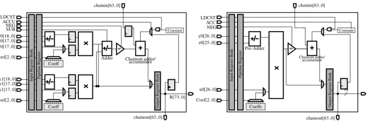
Our work started with the StratixV DSP Block [3] architecture. Although this block has many different modes that users can configure for various applications, we will only describe a subset of features and structures that we can use to build floating point operators. The StratixV DSP Block supports two 18x18 multipliers, which can be used individually, or summed. DSP Blocks can be chained together, for example to implement systolic FIR filters, using dedicated inter-block connections, which are more efficient than using general purpose FPGA routing. The 18x18 multipliers can also be combined
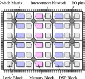
Memory Block Logic Block
Interconnect Network
DSP Block Switch Matrix I/O pins
Chainout adder/ accumulator x1[17..0] y1[18..0] z1[17..0] x0[17..0] y0[18..0] z0[17..0] Constant In p u t R eg is te r B an k P ip el in e R eg is te r SUB chainout[63..0] O u tp u t R eg is te r B an k Adder Coeff Coeff coef[2..0] coef[2..0] NEG ACCU LDCST R[73..0] chainin[63..0]
(a) DSP block in dual 18x18 fixed-point multiplier mode
Chainout adder/ accumulator Constant 64 Pre-Adder Coeffs In p u t R eg is te r B an k P ip el in e R eg is te r chainin[63..0] Coef[2..0] z0[25..0] y0[26..0] NEG ACC LDCST O u tp u t R eg is te r B an k chainout[63..0] x0[26..0]
(b) DSP block in 27-bit fixed-point multiplier mode
Figure 2. DSP block in two fixed-point configurations
...
A B C D AB+CD E F EF+GH G HAB+CD+EF+GH I J IJ+KL+MN+OP
AB+CD 32 32 32 32 32 32 32 32 32 32 32 32 32 32 32 32 IJ+KL AB+CD+EF+GH+IJ+KL+MN+OP EF+GH AB+CD+EF+GH 32 32 32 32
Figure 3. DSP block in Recursive Vector Mode
to create a 27x27 multiplier, which also can be used with the interblock routing. We will build a single precision multiplier based on the 27x27 mode.
3 2 3 2 3 2 3 2
The exception handling and exponent calculation are relatively small and have little effect on area or performance. The critical part of the design is the RNE (round to nearest even) implementation; the pedantic method requires a CPA after the CSA tree of the multiplier, followed by a 1-bit normalization, followed by another CPA for the rounding. The fixed-point modes only need the first CPA; the second CPA would have a significant area and delay impact on them. Although there are many known methods for combining the floating point multiplier CPA and rounding CPA into a single structure, all of the many fixed-point modes still need to be supported. The multiplier pipeline CPA is therefore the most complex portion of the DSP block.
The floating-point adder has no logic or function in common with any of the legacy fixed-point functions, and is imple-mented as a separate block, as FMA is not supported. In Fig. 4, the logical connections between the floating-point multiplier and adder are shown, as well as the connections to and from the adjacent DSP Blocks are shown.
As previously stated, some applications such as matrix decompositions require floating-point arithmetic for handling dynamic range and accuracy. In contrast to traditional FPGA applications such as FIR filters, both the volume of processing (e.g.the size of the dot product for a large matrix calculation, for example), as well as the iterative nature of processing, require a much lower latency. Typically, FPGA implementations of FIR filters use a systolic, or feed-forward flow, which is proportional to one clock per input element; floating point applications containing a long dot product (e.g. 256 elements) cannot wait for 256 cycles between successive intermediate results. A low latency, hardware reduction structures is therefore required.
The reduction structures are based on the adjacent DSP blocks being configured in different modes allowing to input operands from different sources. A logical block diagram, omitting many of the balancing register for illustrative simplicity is shown in Figure 3.
3
Multiplier architecture
There were a number of constraints on the implementation of the floating-point features: (a) full backwards compatibility with the existing fixed-point modes, (b) no performance degradation of the fixed-point modes while operating at similar frequencies for floating-point modes, and (c) only a minimal area increase was allowed. In order to maintain the structure and efficiency of the FPGA, a narrow range of X and Y dimensions are allowable for any embedded block included in the FPGA fabric, which further restricted the scope of the floating-point architectural changes.
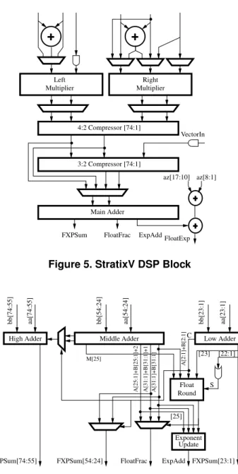
A block diagram of the StratixV DSP Block is shown in Figure 5. Two smaller 18x18 multipliers, preceded by optional input pre-adders, can be used to implement independent multipliers, sums of multipliers, or larger 27x27 multipliers, using the multiplexers and compressors shown in the figure. The final CPA in the DSP Block can be split in two in the case of individual multipliers.
To support all of the fixed-point modes and also floating point multiplication, the final CPA was decomposed into a set of prefix structures aligned with both the fixed and floating-point boundaries. The three floating-point multiplier steps post compression: final sub-product reduction, normalization and rounding were combined into a single-level CPA using a flagged prefix approach [8]. Our flagged prefix approach, in order to support both fixed and floating point calculations, uses a flagged prefix structure, overlaid on the carry-select structure, overlaid on a prefix adder structure. A simplified block diagram of the adder decomposition, without the prefix structures, is shown in Figure 6.
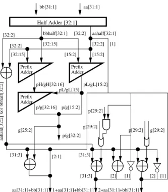
The low adder boundary is the sticky bit boundary. The float/round block uses multiple intermediate values to make a rounding and normalization determination of the floating-point multiplication: the OR of the 22 result bits of the low adder (S), the MSB of the low adder (L[23]), the carry out of the low adder (C), 2 LSBs of the middle adder (M[2:1]) and the MSB of the middle adder when the DSP is in floating-point mode (M[25]). The logic drives the select line of a 3:1 multiplexer (MXSEL) where the output sum is aa+bb+MXSEL. The selection logic is presented in Table 1. When the middle adder is used for floating-point multiplication, a set of half adders is used to first insert a 0 into the LSB of the carry vector input to the middle adder. This is necessary for our flagged prefix approach (+1 and +2) implementation.
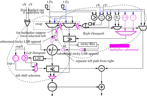
From Figure 7, the two 32 bit sum and carry vectors from the half adders are then input into a prefix network. The prefix network uses a Kogge-Stone architecture and is split two modules, which are required for the independent multiplier fixed-point modes. This prefix network generates two 32 bit carry and propagate vectors. Three values are needed for the floating point multiplier calculation: the 24 bit sum of the inputs, the 23 bit sum plus one, and the 24 bit sum plus two. Depending on the output of the float/round block, along with the 25th bit of the sum, the lower 24 bits of the sum may be normalized by right shifting one bit. The 24 bits sum plus two will therefore become a 23 bit fraction rounded up. The calculation of the three pre-shifted values is shown in Table 2.
Table 1. Float/Round selection logic M[25] M[2:1] C L[23] S MXSEL 0/1 00 0 0 0 0/0 0/1 00 0 0 1 0/0 0/1 00 0 1 0 0/0 0/1 00 0 1 1 1/1 0/1 00 1 0 0 1/1 0/1 00 1 0 1 1/2 0/1 00 1 1 0 2/2 0/1 00 1 1 1 2/2 0/1 01 0 0 0 0/0 0/1 01 0 0 1 0/1 0/1 01 0 1 0 1/1 0/1 01 0 1 1 1/1 0/1 01 1 0 0 1/1 0/1 01 1 0 1 1/1 0/1 01 1 1 0 1/1 0/1 01 1 1 1 2/1 0/1 10 0 0 0 0/0 0/1 10 0 0 1 0/0 0/1 10 0 1 0 0/0 0/1 10 0 1 1 1/0 0/1 10 1 0 0 1/2 0/1 10 1 0 1 1/2 0/1 10 1 1 0 2/2 0/1 10 1 1 1 2/2 0/1 11 0 0 0 0/1 0/1 11 0 0 1 0/1 0/1 11 0 1 0 1/1 0/1 11 0 1 1 1/1 0/1 11 1 0 0 1/1 0/1 11 1 0 1 1/1 0/1 11 1 1 0 1/1 0/1 11 1 1 1 2/1
Table 2. Floating-point CPA Pre-Outputs
Value Result[25:3] Result[2] Result[1]
aa+ bb aa[24:3]half ⊕bb[24:3]half ⊕g[25:2] aa[2]half⊕bb[2]half aa[1]half
aa+ bb + 1 aa[24:3]half ⊕bb[24:3]half ⊕(g[23:2]+ (p[23:2]·aahalf[1])) aa[2]half⊕bb[2]half⊕aa[1]half ¬(aa[1]half)
3:2 Compressor [74:1] Multiplier Right az[8:1] 4:2 Compressor [74:1] Left Multiplier Main Adder VectorIn FloatFrac FXPSum ExpAdd az[17:10] FloatExp
Figure 5. StratixV DSP Block
aa [5 4 :2 4 ] b b [5 4 :2 4 ] b b [2 3 :1 ] aa [2 3 :1 ] aa [7 4 :5 5 ] b b [7 4 :5 5 ]
High Adder Middle Adder
Float Round A [2 5 :1 ]+ B [2 5 :1 ]+ 2 A [3 1 :1 ]+ B [3 1 :1 ]+ 1 A [3 1 :1 ]+ B [3 1 :1 ] Low Adder [22:1] [23] C S A [2 :1 ]+ B [2 :1 ] M[25] Exponent Update ExpAdd FloatFrac FXPSum[74:55] A [2 3 :1 ]+ B [2 3 :1 ] FXPSum[23:1] FXPSum[54:24] [25]
Figure 6. Simplified Final CPA Decomposition. The CPA may also be split in two (not highlighted here for readability) when the DSP block is used in fixed-point mode.
Although only 25 bit outputs are shown, 32 bit results are calculated using the above methods for both aa+bb and aa+bb plus one, as these values are also used for the fixed-point multiplications, as a carry-select adder topology spans across the three adder groups shown in figure 5.
The mantissa of the floating-point multiplication is selected from the three outputs shown in Table 2. There is a small amount of post computation to detect and apply error conditions and exceptions to the floating point multiplier output, but this is trivial in effect compared with the bulk of the multiplication operation. Likewise, the exponent calculation is very small compared to the mantissa multiplication operation, and can be described behaviorally, and therefore implemented by the synthesis tool in the simplest possible structure.
The fixed point multiplications, except for the mode of the two independent 18x18 multipliers, use a single adder result that ranges in width from 38 to 64 bits, and therefore either spans the lower two, or all three adders of Figure 6. The middle and high adders output both aa+bb and aa+bb+1 (the high adder also consists of a flagged prefix adder), which allows a carry
[2] [1] bb[31:1] aa[31:1] Half Adder [32:1] bbhalf[32:1] aahalf[32:1] [15:2] [32:2] [32:15] [32:2] [32:2] [32:15] Prefix Adder Prefix Adder Prefix Adder pH/gH[32:16] p/g[32:16] [15:2] g[25:2] [31:3] aa h al d [3 2 :2 ] x o r b b h al f[ 3 2 :2 ] [32:2] [1] p/g[15:2] p[29:2] pL/gL[15] pL/gL[15:2] p/g[32:2] [1] [2] p[29:2] g[29:2] [31:3] [31:3] g[29:2]
aa[31:1]+bb[31:1] 1+aa[31:1]+bb[31:1] 2+aa[31:1]+bb[31:1]
[2:1]
Figure 7. Middle Adder Flagged Prefix Structure
select network to be constructed from the lowest to highest adder.
In the case of two independent 18x18 multipliers, one of the multipliers uses the low adder and the lower 14 bits of the middle adder, and the other multiplier uses the upper 17 bit of the middle adder and the high adder. The half adders in the middle adder are bypassed in this mode, and the two prefix networks in the adder are separated.
4
Subnormal support
Our floating-point multiplier and adder designs flush subnormal inputs and outputs to zero. We made this choice out of two reasons. Firstly, in an FPGA context most available IP implementations do not support subnormals [9, 10, 11]. Moreover, one of the recent use models for floating-point on FPGAs – OpenCL [12] – does not require subnormal number for achieving single-precision numerical conformance. Secondly, subnormal support in both the adder and multiplier would have too much of a impact on DSP Block size.
Consequently in this section we propose an alternative solution which allows supporting subnormal arithmetic at only a small increase in DPS block size. Our proposed solution consists of an enhanced floating-point adder which supports subnormal arithmetic but which can also function as an external subnormal handling structure for the previous multiplier.
In the following we provide details on how these subnormal handling structures are built. We exemplify for simplicity using a single-path floating-point adder although the reader should note that our DSP Block implementation uses a fast dual-path adder. The dual-path architecture [13] is a textbook implementation that separates an otherwise long critical path consisting of alignment, operation and normalization into two paths: a near path used when inputs are within one exponent difference and have opposite signs (subtraction) and a far path used for the rest of cases. The near path critical path consists of a trivial alignment, a subtraction and a normalization stage whereas the far path consists of an alignment, an operation and a trivial normalization. All in all, the tradeoff between a single-path and a dual path architecture lies in removing an alignment/normalization stage from the critical path. The modifications shown here on the single-path architectures can readily be applied to our dual-path design, or indeed, any other floating point adder design.
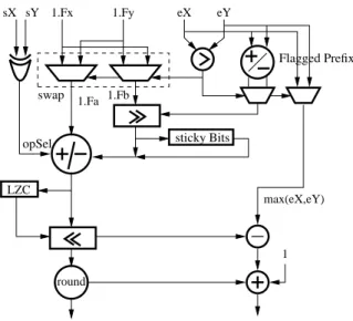
Figure 9 shows a single path FP adder for reference. Two mantissas (1.Fx and 1.Fy) input the first set of multiplexers. Their respective exponents are compared, and the mantissa of the larger value is multiplexed to the left datapath (1.Fa), and the smaller value is multiplexed to the right datapath (1.Fb). Not shown is the comparison between the two mantissas, the
~ M M 1.Fx 1.Fy LZC 1-X multiplier subnormal swap
force selection left for multiplier support subnormal sticky LSB append
round Zero Implied one
if underflow bit
eY eX sX sY
exp-1
subnormal sticky LSB append sticky Bits
separate left path from right
X-1
expX
left shift selection
Right Datapath
Left Datapath
Figure 8. Single-Path floating-point adder with subnormal handling and multiplier subnormal han-dling
result of which is used as a tie-break in case the exponents are equal; by ensuring that the left datapath number is always greater than the right datapath number, a positive output from the fixed-point adder/subtracter is ensured. In the right datapath, the smaller value is shifted to the right (this may be 0 bit positions), and a sticky bit calculated by the ORing of all of the bits shifted to the right of the LSB. The sticky bit is appended to the LSB of the shifted mantissa output of right shifter and added to, or subtracted from, the left datapath value 1.Fa.
The number of leading zeros is counted and the datapath is left shifted so that a ’1’ is present at the implied leading ’1’ position. The following 23 bits are then the pre-rounded mantissa bits, which are rounded using the bits below the LSB of the pre-rounded mantissa bits. Multiple rounding types and techniques are known, and need not be discussed here. The exponent is then updated twice, once during alignment and once post rounding.
In this paper we propose an alternative adder structure, motivated by the lack of subnormal handling support of the pre-sented floating-point multiplier. The difference between this structure and previously reported implementations is therefore the ability of the floating-point adder logic to also be configured as a subnormal handling unit for the multiplier when required. In a configuration where subnormals are supported during multiplication, the floating-point multiplier will use the follow-ing adder in the same DSP Block for subnormal number support. In this use case, the adder is not available for its normal uses such as floating point addition, accumulation, multiply-add, or the recursive modes shown in Section 2. The arrangement of the adder as the multiplier subnormal handler is done at configuration time of the FPGA, and can be independently set for each DSP Block in the device.
4.1
Subnormal number generation from the floating-point multiplier
If the adder is used as a subnormal handler for the multiplier, the multiplier rounding and exception handling stage is bypassed, and a number of signals are forwarded to the adder together with additional generated signals. These include: Forwarded signals :
• the value of the pre-rounded mantissa (MidAdder[25:1])
• the temporary sticky bit OR(LowAdder[22:1])
LZC 1.Fx 1.Fy eX eY 1.Fa 1.Fb sX sY round max(eX,eY) 1 swap sticky Bits opSel Flagged Prefix
Figure 9. Single-Path floating-point adder
• a modified (explained next) value of the exponent used for driving the subnormal stage shifters.
Generated signals :
• a subnormal bit flag, which indicates that a subnormal number has likely been created. The subnormal bit
indi-cates to the adder that the implied ’1’ is not present, and a 0 should be inserted at the appropriate bit position in the datapath instead.
• a negOrZero exponent flag, which indicates that the 8 bit exponent contains a negative number (and not a large
positive number) or that the product exponent pre-normalization is zero;
• an underflow sticky flag, which forwards information the adder may need for a rounding decision;
• an underflow case value. There are six signaled cases, all explained in detail next and synthesized in Table 3.
A subnormal number can only be generated in two cases: the product of two normalized numbers that underflows, or the product of a normalized and a subnormal which underflows. One should note that the product of two subnormal numbers will always generate zero, and even the product of two normalized, or of one normalized and one subnormal number, can also underflow such it produces zero. When it comes to underflow testing, one should also note that the IEEE754-2008 standard [14] is ambiguous about underflow testing: that is, an underflow can be detected either before or after rounding. In our implementation underflow will be detected post rounding.
We next decompose the multiplication operation into its subcomponents – mantissa multiplication and exponent addition
– and evaluate the cases which can generate subnormal outputs, based on the temporary exponent (eX+ eY ) that we refer to
as exponent and the temporary mantissa(mX × mY ) that we refer to as mantissa
For the product of two normalized numbers with mantissas (mX and mY ) ∈[1, 2), the product mantissa (excluding
expo-nent manipulation) is in[1, 4). A subnormal number may be produced in two cases:
Case 1 exponent ≤ 0, 1 ≤ m < 2.
• subnormal flag = 0
• negOrZero exponent = 1
• underflow sticky = sticky OR LowAdder[23].
• exponent = exponent
The adder will right shift by the value 1 − exponent. When the exponent= 0 rounding may bring the result back in the
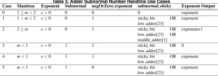
Table 3. Adder Subnormal Number Handline Use Cases
Case Mantissa Exponent Subnormal negOrZero exponent subnormal sticky Exponent Output
0 1 ≤ m < 2 e >0 0 0 0 exponent 1 1 < m < 2 e ≤0 0 1 sticky bit OR low adder[23] exponent 2 2 ≤ m e <0 0 1 sticky bit OR low adder[23] OR middle adder[1] exponent+1 3 m <1 e= 0 1 1 sticky bit OR low adder[23] 0 4 m <1 e <0 1 1 sticky bit OR low adder[23] exponent 5 m <1 e >0 1 0 sticky bit OR low adder[23] exponent Case 2 exponent < 0, m ≥ 2. • subnormal flag = 0 • negOrZero exponent = 1
• underflow sticky = sticky OR LowAdder[23] OR MidAdder[1]
• exponent = exponent + 1
The adder will right shift by the value 1 − exponent.
For the second case when a subnormal output may arise, the multiplication of a normalized number (mantissa ∈[1, 2) with
a subnormal value (mantissa ∈[2−p,1), the mantissa of the product will be in [2−p,2). For a product mantissa ∈ [1, 2) and an
exponent ≥1, the output will be a normalized number so will not need additional handling by the subnormal handling unit
(set underflow flag=0 and negOrZero exponent = 0). If the mantissa ∈[1, 2) and exponent < 1 we apply the rules from Case
1. Otherwise the following cases are possible:
Case 3 exponent= 0, m < 1.
• subnormal flag = 1
• negOrZero exponent = 1
• underflow sticky = sticky OR LowAdder[23].
• exponent = 0
The adder will use the product mantissa for rounding only, since it is already aligned. Case 4 exponent < 0, m < 1.
• subnormal flag = 1
• negOrZero exponent = 1
• underflow sticky = sticky OR LowAdder[23].
• exponent = exponent
The adder will right shift with the value (-exponent) before applying rounding. Case 5 exponent > 0, m < 1.
• subnormal flag = 1
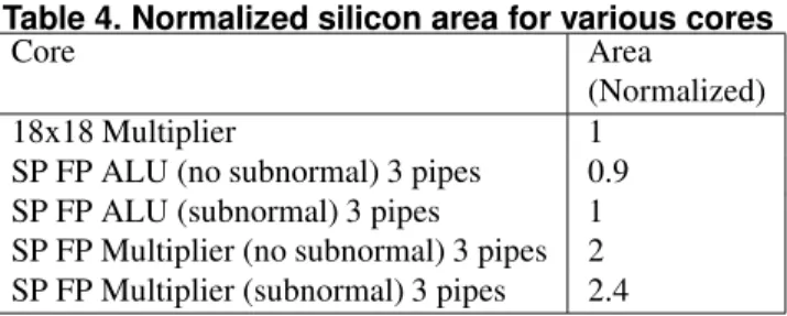
Table 4. Normalized silicon area for various cores
Core Area
(Normalized)
18x18 Multiplier 1
SP FP ALU (no subnormal) 3 pipes 0.9
SP FP ALU (subnormal) 3 pipes 1
SP FP Multiplier (no subnormal) 3 pipes 2
SP FP Multiplier (subnormal) 3 pipes 2.4
• underflow sticky = sticky OR LowAdder[23].
• exponent = exponent
If the number of leading zero of the product ≥ exponent then we left shift by exponent − 1 and set the exponent to zero. Otherwise we normalize and update the exponent.
Figure 8 shows the modifications to the single-path architecture to add subnormal support to an individual multiplier, as well as handle subnormal numbers in the addition/subtraction operation. Both the left and right side of the datapath are used when the adder supports subnormals (including the case where the inputs come from two separate multipliers); the left path and right paths are used independently when the adder is used to support subnormals for a multiplier.
For the floating-point addition, the input AND gates are used to zero the implied leading ’1’ position if the input mantissa has an underflow bit associated with it (input exponent is zero). If the adder is used for the subnormal support for a single multiplier then the select line for the mantissa swapping multiplexers will be forced to select from the left inputs. The subnormal sticky bit from the multiplier is optionally appended to the LSB of the left datapath before the addition/subtraction operation and to the right shifted sticky bit. The values (1-exponent) are calculated using the top-right integer subtracter for cases 1 and 2, together with the negative exponent for case 4, and the appropriate right shift value selected by multiplexer. The left shift can be (exponent-1), for case 5 handled in the left datapath. The AND gates M keeps the two datapaths independent (the right datapath is used in cases 1, 2, 3 and 4, and the left datapath is used in case 5) for multiplier subnormal support. The pre-round multiplexer selects the datapath result to be forwarded to the rounding stage.
5
Results
In this section we present the numbers that allowed adding floating-point support to the DSP block of a commercially viable device. We also present numbers on estimated DSP block increase for supporting subnormals and show how our proposed solution in Section 4 can be a commercially viable solution in terms of area.
The percentage increase of our design (without subnormal support) for adding single-precision floating-point to the DSP block compared to the fixed-point-only implementation has two contributions:
• by reusing the existing fixed-point multiplier structures the floating-point multiplier requires additionally only
ex-ception and exponent handling, normalization and rounding (extending the final fixed-point multiplier adder into a flagged-prefix adder). The logic increase by supporting the floating-point multiplier block is only ≈ 3%.
• the floating-point adder is a stand-alone component. This allows us to optimize its implementation so it takes ≈ 10%.
Between these two contributions the final increase of the DSP block was around 15%, but the effective increase of the entire DSP cost to the FPGA architecture, considering the fixed cost of the existing routing interface, is only about 10%. Depending on the ratio of logic, memory, DSP blocks, and transceivers in a particular device this increase in the DSP block corresponds to an increase between 0.5% and 5% of the die area.
To validate our assumptions about the cost of supporting subnormals we synthesized some fixed and floating-point com-mercial IPs from the Synopsys Design Ware library [15] for 20nm. We report the results, for the same synthesized perfor-mance, area normalized relative only to themselves, in Table 4.
We can see that the subnormal support for a FP multiplier is about half the size of an 18x18 multiplier or an SP FP ALU. This is in line with our expectations, as the subnormal support logic would be approximately the complexity of the near
path of the FP ALU, or the bottom half of a single path FP ALU. These results will not scale directly to our design, as this IP library has all pipelined components, while our FP ALU is combinatorial to support floating point multiply accumulate; achieving the performance of the pipelined multiplier using only combinatorial logic would likely require a larger area.
The three main arithmetic components in our floating point DSP Block are two 18x18 multipliers and one FP ALU. We also need some arithmetic structures equivalent to about half an 18x18 multiplier to combine the two multipliers into one 27x27 multiplier, which is the basis of the FP multiplier. The two multipliers and the FP ALU are approximately the same area, with the FP ALU slightly larger because of the combinatorial area scaling explained above. The relative areas (our functions were all without subnormal support) are similar to the relative areas shown in Table 4. A first order analysis shows that adding subnormal support to both the multiplier and the adder would increase the arithmetic component (other logic and routing is needed to support the configurability of the many options of the DSP Block) of the DSP Block by about 4%, which we felt was not an acceptable penalty for most of the applications we were targeting.
Adding subnormal support directly to the DSP Block would cause other issues, such as the increased propagation delay in the last stage of the DSP Block, which might negatively affect the supported fixed point applications as well. As our FP ALU is combinatorial, the additional area for the ALU might cause a non-linear increase in the area as well.
Our second proposed solution uses the floating-point adder as the subnormal handling unit for the floating-point multiplier. The implies an increase of roughly 10% in the floating-point adder according to Table 4 together with another ≈ 5% required from our experiments for supporting the multiplier subnormal cases. Area alone results show that our proposed solution can provide subnormal support for both the floating-point multiplier and the adder (admittedly, not a the same time) for an extra DSP increase of ≈ 1%.
6
Conclusion
The task of building an FPGA with hardware support for floating-point arithmetic is a research topic that was well ad-dressed in several previous works. A significantly more difficult task is making these choices so that the FPGA is still viable for traditional fixed-point applications. Most previous approaches propose adding the floating-point units as a separate block, possibly grouping them in clusters for increased efficiency. However, when these blocks are unused the FPGA architecture performs sub-optimally both in terms of area as well as power. Our design adds floating-point capabilities to the existing DSP block by reusing and enhancing the fixed-point components such that the cost of floating-point support is a roughly 10% increase in DSP block area. The main challenges are keeping fixed-point performance unaltered, while providing similar floating-point performance, and meeting the area budget. For the floating-point multiplier we had to fuse the rounding stage together with an existing carry-propagate adder – used by the fixed-point modes – by using a flagged-prefix approach in or-der to reduce propagation delay. Our second proposed solution is for adding subnormal support for the ador-der and multiplier. In contrast with adding support for both units, which would involve an additional 4% DSP increase, our proposed solution increases the block size by only 1% more by using the existing floating-point adder having subnormal support as a subnormal handling unit for the floating-point multiplier.
References
[1] F. de Dinechin, B. Pasca, O. Cret¸, and R. Tudoran, “An FPGA-specific approach to floating-point accumulation and sum-of-products,” in IEEE International Conference on Field-Programmable Technology. IEEE, 2008, pp. 33–40.
[2] F. de Dinechin and B. Pasca, “Floating-point exponential functions for DSP-enabled FPGAs,” in IEEE International Conference on Field-Programmable Technology. IEEE, 2010.
[3] M. Beauchamp, S. Hauck, K. Underwood, and K. Hemmert, “Architectural modifications to enhance the floating-point performance of FPGAs,” Very Large Scale Integration (VLSI) Systems, vol. 16, no. 2, pp. 177–187, Feb 2008.
[4] C. Ho, P.-W. Leong, W. Luk, S. J. E. Wilton, and S. Lopez-Buedo, “Virtual embedded blocks: A methodology for evaluating embedded elements in fpgas,” in Field-Programmable Custom Computing Machines, 2006. FCCM ’06, April 2006, pp. 35–44.
[5] C. H. Ho, C. W. Yu, P.-W. Leong, W. Luk, and S. J. E. Wilton, “Domain-specific hybrid FPGA: Architecture and floating point applications,” in Field Programmable Logic and Applications, 2007. FPL 2007. International Conference on, Aug 2007, pp. 196–201.
[6] Y. J. Chong and S. Parameswaran, “Configurable multimode embedded floating-point units for FPGAs,” Very Large Scale Integration (VLSI) Systems, IEEE Transactions on, vol. 19, no. 11, pp. 2033–2044, Nov 2011.
[7] C. H. Ho, C. W. Yu, P. Leong, W. Luk, and S. J. E. Wilton, “Floating-point FPGA: Architecture and modeling,” Very Large Scale Integration (VLSI) Systems, IEEE Transactions on, vol. 17, no. 12, pp. 1709–1718, Dec 2009.
[8] N. Burgess, “The flagged prefix adder and its applications in integer arithmetic,” J. VLSI Signal Process. Syst., vol. 31, no. 3, pp. 263–271, July 2002. [Online]. Available: http://dx.doi.org/10.1023/A:1015421507166
[9] LogiCORE IP CORDIC v7.0, 2013, http://www.xilinx.com/support/documentation/ip documentation/floating point/v7 0/pg060-floating-point.pdf. [10] “Megawizard plug-in manager,” http://www.altera.com.
[11] F. de Dinechin and B. Pasca, “Designing custom arithmetic data paths with FloPoCo,” IEEE Design and Test, 2011.
[12] Khronos OpenCL Working Group, The OpenCL Specification, version 1.0.29, 8 December 2008. [Online]. Available: http://khronos.org/registry/cl/ specs/opencl-1.0.29.pdf
[13] M. D. Ercegovac and T. Lang, Digital Arithmetic. Morgan Kaufmann Publishers, 2004. [14] “IEEE Standard for Floating-Point Arithmetic,” IEEE Std 754-2008, pp. 1–58, 29 2008.
[15] “DesignWare Library – Datapath and Building Block IP,” https://www.synopsys.com/dw/buildingblock.php.
[16] P. M. Farmwald, “On the design of high performance digital arithmetic units,” Ph.D. dissertation, Stanford, CA, USA, 1981, aAI8201985.
[17] P.-M. Seidel and G. Even, “On the design of fast ieee floating-point adders,” in Computer Arithmetic, 2001. Proceedings. 15th IEEE Symposium on, 2001, pp. 184–194.
[18] ——, “Delay-optimized implementation of ieee floating-point addition,” IEEE Trans. Comput., vol. 53, no. 2, pp. 97–113, Feb. 2004. [Online]. Available: http://dx.doi.org/10.1109/TC.2004.1261822
![Table 1. Float/Round selection logic M[25] M[2:1] C L[23] S MXSEL 0/1 00 0 0 0 0/0 0/1 00 0 0 1 0/0 0/1 00 0 1 0 0/0 0/1 00 0 1 1 1/1 0/1 00 1 0 0 1/1 0/1 00 1 0 1 1/2 0/1 00 1 1 0 2/2 0/1 00 1 1 1 2/2 0/1 01 0 0 0 0/0 0/1 01 0 0 1 0/1 0/1 01 0 1 0 1/1 0/1](https://thumb-eu.123doks.com/thumbv2/123doknet/12768273.360236/6.892.320.572.201.682/table-float-round-selection-logic-m-m-mxsel.webp)