Charge Detection in Semiconductor
Nanostructures
by
Kenneth MacLean
B.S. in Physics and Mathematics, Yale University, 2002
Submitted to the Department of Physics
in partial fulfillment of the requirements for the degree of
Doctor of Philosophy
at the
MASSACHUSETTS INSTITUTE OF TECHNOLOGY
N'OV
8
/2~
Li
ARCHIVES
February 2010
0
Massachusetts Institute of Technology 2010. All rights reserved.
A u th o r . . . .. . . . .
Department of Physics
November 4, 2009
Certified by...
...
Marc A. Kastner
Donner Professor of Science and Dean of the School of Science
Thesis Supervisor
-A!/Accepted by .
Krishna Rajagopal
Professor of Physics and Associate Department Head for Education
Charge Detection in Semiconductor Nanostructures
by
Kenneth MacLean
Submitted to the Department of Physics on November 4, 2009, in partial fulfillment of the
requirements for the degree of Doctor of Philosophy
Abstract
In this thesis nanometer scale charge sensors are used to study charge transport in two solid state systems: Lateral GaAs quantum dots and hydrogenated amorphous silicon (a-Si:H). In both of these experiments we use time-resolved charge sensing to study electron transport in regimes that are not accessible to traditional transport measurements.
For the lateral GaAs quantum dot experiments, we use a GaAs quantum point contact integrated with the dot as a charge sensor. We use this sensor to observe single electrons hopping on and off the dot in real time. By measuring the time intervals for which the dot contains one and zero electrons, we probe the rate F at which electrons tunnel on and off the dot from the leads. We measure F as a function of the drain source bias V, and gate voltages V applied to the dot. At zero magnetic field, we show that the dependencies of F on Vda and V can be understood in terms of a simple quantum mechanical model which takes into account variations in the electron energy relative to the top of the tunnel barriers separating the dot from the leads. We also show that the tunneling is dominated by elastic processes. At high magnetic fields, we show that tunneling into the excited spin state of the dot can be completely suppressed relative to tunneling into the ground spin state. The extent of the suppression depends on the shape of the electrostatic potential defining the quantum dot.
For the a-Si:H experiments, we pattern a nanometer scale strip of a-Si:H adja-cent to a narrow silicon MOSFET (metal-oxide-semiconductor field-effect transistor), which serves as an integrated charge sensor. We show that the MOSFET can be used to detect charging of the a-Si:H strip. By performing time-resolved measurements of this charging, we are able to measure extremely high resistances (~ 1017 Q) for the a-Si:H strip at T ~ 100 K. At higher temperatures, where the resistance of the a-Si:H strip is not too large, we show that the resistances obtained from our charge detection method agree with those obtained by measuring current. Our device geometry allows us to probe a variety of electron transport phenomena for the a-Si:H, including the field effect and dispersive transport, using charge detection. We extract the density of localized states at the Fermi level for the a-Si:H and obtain consistent results. We
discuss the effect of screening by the substrate on the sensitivity of the MOSFET to charge in the a-Si:H, and show that the MOSFET can detect switching noise in the a-Si:H.
Thesis Supervisor: Marc A. Kastner
Acknowledgments
When I was about to start graduate school, I pictured spending long hours working alone in a laboratory in some basement, and worried I would feel extremely isolated.
My experience in graduate school was nothing like this, and looking back, what I
remember most about my time at MIT are the people I was surrounded by, to many of whom I owe a great deal of gratitude.
I would first like to thank my research adviser, Marc Kastner. Before I started at MIT, I do not think I realized how crucial my choice of research adviser would be to
my experience in graduate school. Looking back now, my experience working with Marc was so positive that it is hard for me to know how to begin thanking him. Marc is an excellent leader, and a truly inspiring person to work with. I will be forever indebted to him for teaching me how to think about physics and providing an ideal environment in which to do creative research.
All of the work I did at MIT was done in collaboration with a number of other
scientists. When I first got to MIT I started working on experiments involving lateral GaAs quantum dots with Sami Amasha, who was a few years into graduate school at that time. I can't say enough about Sami. He is an extremely talented physicist and a great guy, both of which facts are obvious to anyone who has worked with him for an hour or two. Early on, when I did not have much experience working in a laboratory, Sami took a huge amount of time to show me how to design and execute experiments. As time went on our collaboration became very productive. We worked on a number of interesting experiments, all of which drew heavily on ideas we had been bouncing back and fourth, usually while transferring Helium or performing similar routine laboratory tasks. I also worked with two other members of the Kastner group on the GaAs quantum dot portion of my thesis, Dominik Zumbiihl and Iuliana Radu, who fabricated the samples we used for our experiments. Dominik was a post doc in our group at this time, and was a great source of guidance. Iuliana is a great physicist and a really fun person to work with. Throughout graduate school,
good perspective on virtually anything. I also want to thank Micah Hanson ant Art Gossard for growing the excellent heterostructures we used for our devices, without which none of our GaAs quantum dot experiments would have been possible.
As my work on GaAs quantum dots began to come to a close, I started working with Tamar Mentzel, and Moungi Bawendi, Scott Geyer, and Venda Porter, our col-laborators in the chemistry department, on arrays of semiconducting nanocrystals, and I really enjoyed participating in this facet of our group's research. Following this work, Tamar and I collaborated closely, working on silicon charge sensors. This col-laboration was extremely rewarding. Tamar is an outstanding physicist, and working together we were able to learn silicon fabrication and a number of other techniques that were new to both of us in a short amount of time. This was facilitated in large part by Tamar's creativity, which kept our project moving along quickly despite the number of obstacles we ran into along the way. Tamar is also a great friend. I also want to thank the staff of the MTL for their help with our MOSFET fabrication.
There are a number of other members of the Kastner group who helped me during the course of my Ph.D. Andrei Kogan and Ghislain Granger were members of the group during the beginning of my Ph.D. and they both taught me a lot about research
in our laboratory. Ian Gelfand started as a graduate student around the same time I did. We shared an office together and I enjoyed discussing science and other things with him over the years. Colin Dillard started a few years after me and has been a great person to work with. Within the last two years, our group has been fortunate to get two excellent post-docs, Jingshi Hu and Xi Lin. I been lucky to work with Jingshi a bit on his silicon germanium work. His work is very impressive, and he has moved a very difficult project ahead a lot in a short time frame. I have enjoyed getting to know Xi over the past year, he is a great person to ask for advice, and I am looking forward to seeing whether we can combine some of the techniques Tamar and
I developed with the systems he and Colin are investigating. Our group has also been
fortunate to have two new graduate students, Nirat Ray and Andrew Lai, who I am looking forward to getting to know. I also want to thank the undergraduate students who worked with Sami and I on the GaAs quantum dot project: Anat Burger, Jessica
Schirmer, and Vladimir Rosenhaus.
There are a number of scientists outside of our group who helped me a lot with my research during my time at MIT. I frequently consulted Ray Ashoori and Leonid Levitov, my thesis committee members, about my research and received excellent insight and advice. I also want to thank Juan Climente, Andrea Bertoni, Guido Goldoni, Vitaly Golovach, Daniel Loss, Emmanuel Rashba, Jeff Miller, Oliver Dial, Jae-kyu Lee, Bertrand Halperin, Mark Rudner, Helmut Fritzsche, and Jim Kakalios, for fruitful discussions about the work presented in this thesis.
I want to thank all of my friends and family. I can't thank all of my friends
sufficiently in writing, but they know who they are and how I feel about them. I want to thank my fiance Abby, who is the best thing to happen to me in graduate school, or in my life for that matter, and I want to also thank Abby's family. I want to thank my parents, Bec, Lizzie and Brendan, Kevin, all of my nieces and nephews, Atara and Megan and their families. Lastly I want to thank my sister Mary. I miss her very much.
Contents
1 Introduction
2 Energy Dependent Tunneling at Zero Magnetic Field
2.1 Introduction: GaAs Quantum Dots . . . . 2.2 Charge Detection Measurement... . . . . . . . . 2.3 Energy Dependent Tunneling: Drain-Source Bias Dependence . . . .
2.4 Gate Voltage Dependence . . . .
3 Spin Dependent Tunneling in Large Magnetic Fields
3.1 Measurement and Magnetic Field Dependence of
x
. . . ...
3.2 Shape Dependence of Spin Dependent Tunneling . . . . 3.3 Closing Remarks on Charge Detection with GaAs Nanostructures . .
4 Charge Detection Using a Narrow MOSFET
4.1 Introduction: MOSFET Physics ...
4.2 MOSFET Fabrication . . . . 4.3 Patterning Hydrogenated Amorphous Silicon . . . . 4.4 Instrumentation.... . . . ..
4.5 Electrical Characteristics . . . . 4.6 Noise Properties . . . . 4.7 GaAs QPCs and Narrow MOSFETs: A Brief Comparison.
5 Detecting Charge in an Amorphous Semiconductor 5.1 Introduction . . . ... 59 . . . . 60 . . . . 63 . . . . 65 . . . . 70 . . . . 75 . . . . 79 . . . . 84
5.2 5.3 5.4 5.5 5.6 5.7 5.8
5.1.1 Electronic Properties of a-Si:H . . . .
5.1.2 Measuring Electron Transport in Resistive Materials Charge Detection Technique . . . . Diffusion Model . . . . . . . ..
Temperature Dependence . . . .
F ield E ffect . . . . Dispersive Transport... . . . . . . ..
Screening Effects. . . . . . . ..
a-Si:H IV Characteristics and Noise Correlations . . . .
. . . . 88 . . . . 92 . . . . 94 . . . . 97 . . . . 100 . . . . 102 . . - 104 108 . . . . 113 6 Conclusion A Fabrication
A.1 MOSFET Fabrication. . . . . A.2 a-Si:H Patterning . . . . A.3 Electron Beam Lithography . . . .
117
123 123 132
List of Figures
Lateral GaAs Quantum Dots. . . . . Device and Measurement Circuit . . . . M\easurement Details... . . . . . . . . ..
Drain-Source Bias Dependence . . . . Drain-Source Bias Dependence: Detailed Model... ..
Gate Voltage Dependence Measurement . . . . Gate Voltage Dependence . . . . Measurement of Tunneling in a Magnetic Field . . . . X vs. M agnetic Field. . . . ..
Pulsed Gate Technique for Measuring Orbital Excited States
x vs. Shape . . . . 2-1 2-2 2-3 2-4 2-5 2-6 2-7 3-1 3-2 3-3 3-4 4-1 4-2 4-3 4-4 4-5 4-6 4-7 4-8 4-9 4-10
4-11 MOSFET Trap Tunneling Lineshape
Sketch of MOSFET . . . . Device sketch after polysilicon deposition . . . . Images of Device After MOSFET Fabrication . Doping Hydrogenated Amorphous Silicon . . . . Hydrogenated Amorphous Silicon Test Patterns Electron Micrograph of Device . . . . Measurement Circuit. . . . ..
Noise Analysis . . . . MOSFET Conductance vs. Gate Voltage . . . .
MOSFET Telegraph Noise . . . .
. . . . . 23 . . . . . 26 . . . . . 28 . . . . . 32 . . . . . 35 . . . . . 38 . . . . . 40 . . . . . 45 47 . . . . . 50 . . . . . 53 . . . . . . . . . 62 . . . . 64 . . . . 66 . . . . 68 . . . . 69 . . . . 70 . . . . 72 . . . . 73 . . . . 76 . . . . 80 . . . . 8 2
4-12 MOSFET and GaAs Charge Sensors . . . .8
5-1 The Electronic Structure of Amorphous Materials . . . . 90
5-2 Device and Measurement Technique.. . . . . . . . . 96
5-3 Charge Diffusion Model... . . . . . . . . 98
5-4 Conductance vs. Temperature . . . . 101
5-5 Field Effect... . . . . . . . . . . . . 103
5-6 Hysteresis... . . . . . . . .. 106
5-7 Dispersive Transport... . . . . . . .. 107
5-8 Measurement of Screening... . . . .. 109
5-9 Signal Size Variations . . . 111
5-10 a-Si:H Current vs. Voltage Characteristics . . . . 114
5-11 Noise Correlations... . . . . . . . . 115
Chapter 1
Introduction
One of the most important properties of semiconducting materials is their sensitivity to relatively small changes in charge density. For a pure semiconductor crystal, the Fermi level lies in the middle of the band gap, so that the charge density in the conduction and valence bands is very small, and the conductivity of the material is very low. What distinguishes such a material from an insulator is that for a semiconductor, a modest change in the electrostatic environment of the crystal, in the form of an applied electric field, a small number of impurity atoms introduced into the crystal, or exposure to electromagnetic radiation, creates a change in the charge density in the conduction or valence band that has a dramatic effect on the conductivity. This sensitivity leads directly to the wide variety of semiconductor transistors, diodes, and photovoltaic devices that, since the invention of the solid state transistor [1], have come to dominate modern electronics [2].
As semiconductor technology has matured and miniaturized, techniques for sculpt-ing materials on smaller and smaller length scales have developed. Empowered by this technology, physicists have explored the behavior of electrons confined to nanometer scale semiconductor devices. Electrons confined to small solid state structures, re-ferred to as quantum dots, behave much like electrons occupying the orbitals of single atoms [3]. A variety of experiments have explored aspects of this atomic behavior
[4, 5, 6, 7, 8]. Electrons occupying quantum dots can be coupled through tunnel bar-riers to a Fermi sea, and this has lead to the observation of other interesting physical
phenomena, including the single electron transistor functionality of quantum dots [9], and many-body electron interactions involving electrons on the quantum dot and in the leads [10, 11]. In addition to quantum dots, where the electronic wavefunction is confined in all three dimensions, structures that confine electrons in only two dimen-sions have also been studied extensively, revealing a number of interesting effects to solid state physicists [12, 13].
The conductivity through all nanoscale semiconductor devices is enormously sen-sitive to the electrostatic environment of the device. This fact was reported almost as soon as physicists began fabricating semiconducting devices of a sufficiently small size [14] and is fairly obvious to any experimentalist who has observed the "switch-ing" behavior evident to some extent in all of these devices [15, 16]. In fact, the
electric field generated by a single electron in the immediate vicinity of a nanoscale semiconductor device creates a measurable change in the device conductivity. For example, for a nanoscale MOSFET (metal-oxide-semiconductor field-effect transis-tor), the conductivity is sensitive to the occupation of single defects in the oxide near the oxide-semiconductor interface. This sensitivity can be used to study electrons confined to these defects, and has been utilized to observe a wide range of interesting effects, from many body electron-electron interactions [17] to the spin resonance of a
single electron spin [18].
As nanometer semiconductor devices were further developed, it was demonstrated that they could function as ultra-sensitive electrometers, capable of detecting not only single electron fluctuations within the device itself, but also in structures adjacent to the device [19]. Nanometer scale semiconductor devices functioning as electrometers, patterned adjacent to a structure of interest, are called integrated charge sensors. In the work reported in this thesis, we use integrated charge sensors to study two very different systems: Lateral GaAs quantum dots and hydrogenated amorphous silicon (a-Si:H). Specifically, in Chapters 2 and 3, we report measurements of single electron tunneling in GaAs quantum dots obtained using a GaAs quantum point contact as an integrated charge sensor, and in Chapters 4 and 5 we report measurements of electron transport in a-Si:H obtained using a nanometer scale MOSFET as an
integrated charge sensor.
Lateral GaAs quantum dots are one of the most well understood nanometer scale semiconducting devices [20]. Integrated charge sensors were first demonstrated for this system [19], in the form of a nanometer scale conducting channel, or quantum point contact (QPC), positioned adjacent to the dot. Recently, some time after the initial report of the integrated charge sensor, a number of research efforts have demonstrated that integrated charge sensors can be used to study aspects of the quantum mechanical behavior of electrons confined to GaAs quantum dots that are impossible to observe
by directly measuring the current flowing through the dot [21, 22, 23, 24, 25]. The
work reported in Chapters 2 and 3 constitute part of this initiative. Specifically, we use integrated charge sensors to reveal fundamental aspects of the way in which electrons tunnel on and off a GaAs quantum dot.
In Chapter 2, we discuss the techniques we have developed for using integrated charge sensors to study GaAs quantum dots, and use them to study the tunneling process at zero magnetic field. We demonstrate that the tunneling is dominated by elastic processes, and that variations in the tunnel rate as the drain-source-bias and gate voltages applied to the quantum dot are changed can be described by a simple quantum mechanical model that takes into account variations in the electron energy relative to the tunnel barrier potential.
In Chapter 3, we examine the tunneling process in the presence of a large magnetic field. Surprisingly, we find that as the magnetic field is increased, tunneling into the excited spin state can be completely suppressed relative to tunneling into the ground spin state. The extent of this suppression varies as the shape of the quantum dot is changed. While the phenomenology of this effect is clear, these results have not as of yet been explained theoretically. The experiments presented in Chapters 2 and 3, enabled by the integrated charge sensing technique, contribute to a full understanding of the physics of tunneling in quantum dots, a process that is central to all applications of these devices. Having seen the substantial impact of the integrated charge sensor on transport studies of quantum dots, we sought to use these sensors to study electron transport in other solid state systems.
One aspect of the integrated charge sensing technique that stands out in contrast to the measurement of current is its ability to measure extremely slow electron dy-namics. Current, a measure of charge per unit time, becomes immeasurably small for systems where electrons move slowly. Replacing the measurement of current with a time-resolved measurement of charge, one obtains a probe of electron transport that is ideally suited for the study of slow electron dynamical processes. It is in part this aspect of the integrated charge sensing technique that has resulted in its large impact on the study of GaAs quantum dots, as it allows the experimenter to study transport in dots that are almost completely isolated from the Fermi sea in their leads.
In Chapters 4 and 5 we exploit the ability of integrated charge sensors to measure slow electron dynamics, and use this technique to probe electron transport in highly resistive materials for which traditional transport techniques fail. As a resistive ma-terial, we use a nanometer scale strip of a-Si:H, cooled to a temperature where the resistance is very high. Having demonstrated the application of integrated charge sensing to the study of a-Si:H, a material for which the electronic structure has been studied extensively [26], we anticipate that our work will be extended to characterize the electronic properties of other technologically significant materials for which a high electrical resistance inhibits the measurement of current.
Chapter 4 is the most technical chapter of this thesis. It covers the fabrication, instrumentation, and electrical characteristics of the narrow MOSFET sensor and a-Si:H strip. Since over the past five years many studies of electron transport in GaAs quantum dots utilizing a QPC as an integrated charge sensor have been reported, and technical aspects of such experiments are now well documented [27, 28, 29]. However, our work with a-Si:H is the first utilization of integrated charge sensors for the study of resistive materials, so a presentation of the technical aspects of these experiments is well warranted.
In Chapter 5, we present our measurements of transport in a-Si:H, obtained using a narrow MOSFET as an integrated charge sensor. We are able to measure incredibly high resistances (~ 1017 Q) for the a-Si:H strip, using only moderate voltages (~ 1 volt). Our technique allows us to probe a variety of transport phenomena, including
the temperature, electric field, and time dependence of the transport, using charge sensing. We extract the density of states at the Fermi level for the a-Si:H and obtain consistent results. Our measurements are also consistent with the standard model for electron transport in a-Si:H [26]. The work presented in this chapter constitutes a fundamentally new way of measuring electrical resistance that is ideally suited to the study of electron transport in highly resistive thin film materials.
In Chapter 6, we discuss the broader implications of the work presented in this thesis, and present ideas for future experiments.
Chapter 2
Energy Dependent Tunneling at
Zero Magnetic Field
In this chapter we discuss time-resolved measurements of single electron tunneling in a GaAs quantum dot at zero magnetic field. In Section 2-1, we give an introduction to lateral GaAs quantum dots. In Section 2.2 we describe how we measure the charge on the dot using a quantum point contact (QPC) charge sensor, and show how we use time-resolved charge detection to measure the tunneling rate F between the dot and its leads. In Section 2.3, we measure the dependence of F on drain-source bias Vd8, and show that this dependence can be explained in terms of elastic tunneling at a rate set by the difference between the electron energy and the height of the tunnel barrier, a process we will refer to as energy dependent tunneling. In Section 2.4, we measure the dependence of F on plunger gate voltage V, and show that this dependence can also be understood in terms of energy dependent tunneling. Parts of the results presented here appear also in K. MacLean et al. [30].
2.1
Introduction: GaAs Quantum Dots
A quantum dot is a nanometer scale region of semiconductor to which a small number
of electrons are localized, and for which both the Coulomb energy Ec required to add an additional electron, and the energy splitting between different quantum orbital
states EQ play an important role. Because Ec = 2
/C,
where C is the capacitance of the dot, and EQ ~h
2/2rn*L
2,
where m* is the electron effective mass and L is the size of the dot, EQ and Ec become larger the smaller L and C, which are both reduced by making the dot smaller. Quantum dots are therefore constructed using nanofabrication techniques.The variety of ways in which quantum dots can be fabricated can roughly be divided into two categories. For the first category, small chunks of semiconductor of various sizes and shapes are grown using chemical processes. For the second category, the quantum dot is patterned using nanolithographic techniques. These two categories can overlap. For instance, a number of groups have studied surface gated carbon nanotubes [31, 32]: For these devices, the carbon nanotube is grown by chemical vapor deposition, and the gates are then patterned around the nanotube using electron beam lithography.
Very small nanostructures can be made with chemical processes, and the energy scales Ec and EQ for quantum dots made with these processes can be quite large. The effect of quantum confinement can be observed at room temperature and can play an important role in how these dots interact with electroniagnetic radiation in the optical and infrared frequency ranges [33, 34]. Quantum dots fabricated with nanolithography are generally larger, so that Ec and EQ are smaller, and the effects of quantum confinement and Coulomb repulsion are observable only at cryogenic temperatures. Transitions between the quantum energy levels of these dots are usually driven with lower frequency radiation, in the microwave range [35, 36].
For quantum dots fabricated with nanolithography, surface gates patterned adja-cent to the dot can be used to tune the properties of the quantum dot. This tunablity has enabled a wide variety of experiments. For instance, for lateral GaAs quantum dots, one can control in-situ the rate of tunneling F coupling the dot to its leads: F can be adjusted over more than ten orders of magnitude by changing the voltages applied to the gates that define the tunnel barriers of the quantum dot. Because of this tunability, this type of quantum dot has been used to study correlated-electron physics [10, 11], which becomes important when the coupling of the dot to its leads
is strong, and also the coherence of electron charge and spin states [7, 22, 37], which can be maintained only when the coupling to the leads is weak.
The experiments discussed in this chapter are performed with a lateral GaAs quantum dot (Fig. 2-1) fabricated with electron beam lithography. To make such a device, we start with a heterostructure grown by molecular beam epitaxy consisting of GaAs topped with a thin (110 im) layer of AlGaAs (more precisely, Alo.3Gao.7As),
as depicted in Fig. 2-1(a). Within the AlGaAs, a distance dd = 60 nm from the
GaAs/AlGaAs interface, there are a small number of silicon atoms (less than one atomic layer). The silicon acts as an electron donor in GaAs. Because the conduction band of AlGaAs lies above the conduction band of GaAs by an amount eVb, ~ 240 meV, a number of electrons donated by the silicon atoms will move into the GaAs. The positively charged ionized silicon donors left behind in the AlGaAs create a strong electric field that pulls these electrons to the GaAs/AlGaAs interface. These electrons, confined to within ~ 5 nim of the GaAs/AlGaAs interface, form a two dimensional electron gas (2DEG). The number of electrons per unit area ne in the 2DEG is given
by the amount of charge required to charge the capacitance Cd between the silicon
donor layer and the GaAs/AlGaAs interface up to a voltage equal and opposite to the potential difference between the AlGaAs and GaAs conduction bands:
en = CdVbo (2.1)
Here Cd = onA/dd, where here nA is the dielectric constant of AlGaAs. For the heterostructure used in our experiments, ne = 2.2 x 10" em-2. The conductance per square of the 2DEG is given by:
u = enep (2.2)
Here p is the mobility of the 2DEG, which for our sample is equal to 6.4x 10⁵
cm2
/Vs [38]. A high mobility reflects a small amount of scattering for electrons in the
'This value was obtained from Hall effect data by G. Granger [38]. The value calculated from Eqn. 2.1 differs by only 25 %.
2DEG, which leads to a high conductance. The GaAs/AlGaAs structures discussed
here have mobilities that are quite high compared to 2DEGs in other semiconductor structures (Chapter 4). This is a result of the fact that AlGaAs and GaAs are lattice matched, so that there are very few dangling bonds, dislocations, or other defects near the AlGaAs/GaAs interface, and the fact that the silicon dopants are physically separated from the 2DEG.2 There are therefore few potential fluctuations off of which
to scatter. Because of their high mobility, these type of heterostructures are used in high electron mobility transistors (HEMT) and other devices designed to operate at high frequencies for which a high conductivity is desired [40, 41].
The heterostructure provides one dimension of confinement. To confine the elec-trons in the other two dimensions, we pattern nanometer scale metallic gates on the surface of the heterostructure.3 A micrograph of the gate structure is shown in Fig. 2-1(b). We apply negative voltages to the top five gates (SG1, LP1, PL, LP2, and SG2) and to the gate OG. This depletes the electrons in the 2DEG underneath these
gates. As the voltages are made more negative, the electrons in the regions between
OG and SG1 and between OG and SG2 are depleted, forming two tunnel barriers.
The region between the two tunnel barriers, indicated by the blue oval in Fig. 2-1(b), constitutes the quantum clot.
The potential as a function of position taken along the dashed green curve in Fig.
2-1(b) is shown in Fig. 2-1(c). There are two tunnel barriers where the potential
rises above the Fermi level in the 2DEG. These barriers separate the potential well in between them from the two Fermi sea leads, forming the quantum dot confining potential. The potential at the bottom of the well can be shifted relative to the Fermi level in the leads by adjusting the voltages applied to the three gates LP1, PL, and LP2, so that the number of electrons on the dot can be controlled. We refer to these three gates as the plunger gates, and we apply approximately the same gate voltage V to each of them for all of the experiments discussed here. This is done so that there is only one potential minimum between the two tunnel barriers.
2
This type of doping is referred to as modulation doping [39].
w. .... ... .. ... ... ... ..
(a)
(b)
SG1i
LP1PLLP2
SG2
-QG2
100
nm
(c)
OG
(d)
Figure 2-1: (a) Cross section of the GaAs/AlGaAs heterostructure and a nanopat-terned metallic gate, as discussed in the main text. The top of the heterostructure has a thin 10 nm capping layer of GaAs. The gates consist of gold on top of a thin titanium layer, the latter of which adheres well to the GaAs cap [29]. (b) Electron micrograph of our lateral GaAs quantum dot gate structure. The gates with pink x's over them are kept grounded for all of the experiments discussed here and can be ignored. Negative voltages are applied the gates OG, SG1, LP1,PL, LP2, and
SG2, forming a quantum dot at the position of the blue oval. A negative voltage
is also applied to the gate QG2 to create a quantum point contact charge sensor as discussed in Section 2.2. (c) Sketch of electrostatic potential U(x) in the 2DEG along the dashed green curve in (b). The Fermi seas in the two leads are separated from the quantum dot by two tunnel barriers. The one and two electron states of the quantum dot are indicated by the lower and upper solid blue lines. The dashed black line indicates a single electron excited orbital state. The dashed green line indicates the single electron excited spin state in the presence of a magnetic field. (d) Simple model for localization of electrons on a quantum dot, as discussed in the main text.
The relevant energy scales for the quantum dot system are sketched in Fig. 2-1(c). The largest energy scale is the Fermi level EF relative to the bottom of the conduction band, which can be calculated from the electron density in the 2DEG, and is approximately 7 meV. Next largest is the Coulomb energy Ec ~ 4 meV required to add an additional electron to the quantum dot. This energy is given by the difference in energy between the one and two electron states, sketched as the solid blue lines in Fig. 2-1(c). For all of the experiments discussed here, the two electron state is above
EF, so that there is either one or zero electrons on the quantum dot.
The next largest energy scale is the quantum confinement EQ, which is given by the difference between the energy of an excited orbital state (dashed black line in Fig. 2-1(c)) and the ground state. Of course, there are a number excited orbital states. For lateral quantum dots, the confinement created by the heterostructure along the direction perpendicular to the GaAs/AlGaAs interface is typically much stronger than the confinement created by the gates. For low energy excitations, one can therefore model the quantum dot confining potential as a two dimensional harmonic oscillator potential well. For our device, the excited state of this harmonic oscillator with the smallest energy is ~ 2 meV above the ground state, as we will see in the following sections.
For the experiments discussed in the following chapter, we apply a magnetic field
B in the plane of the 2DEG. For these experiments, where typically B is a few Telsa,
there is an excited spin state ~ 100 peV above the ground spin state. This state is sketched as the dashed green line in Fig. 2-1(c). Finally the smallest energy scale is
kT.
This energy scale determines the broadening of the Fermi distribution function in the leads (not shown in Fig. 2-1(c)). All of the experiments discussed here are performed in an Oxford 75 pW dilution refrigerator, at an electron temperature T -120 mK so thatkT
~ 10 pV is much smaller than any of the other relevant energy scales.In the following sections, we use time resolved single electron charge sensing to study the tunneling process by which electrons move on and off the quantum dot. For these experiments, the tunnel barrier resistances Rb are very large. Before turning to
a discussion of these experiments, we discuss a fundamental question: How resistive do the tunnel barriers need to be in order for charge to be localized on the quantum dot in the first place? To provide an intuitive answer to this question, we consider a quantum dot connected to a grounded, Fermi Sea lead through one tunnel barrier of resistance Rb (Fig. 2-1(d)). The time it takes to charge the quantum dot is given
by T - RbC, where here C is the capacitance of the dot to ground. In order for localization to occur, the Coulomb charging energy of the dot, Ec = e2/C, must be larger than the time-energy uncertainty 6E ~ h/T ~ h/RbC. From this we obtain the minimum barrier resistance necessary for localization to be Rb ~ h/e2, the inverse
of the quantum conductance.
2.2
Charge Detection Measurement
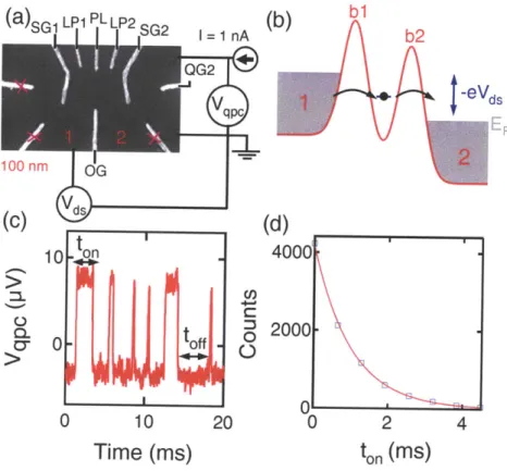
For the experiments discussed in the following sections, we utilize time-resolved single electron charge detection. Our measurement circuit is shown Fig. 2-2(a). Applying a negative voltage to the gate QG2, we form a quantum point contact (QPC) be-tween the gates QG2 and SG2. The device characteristics of quantum point contacts will be discussed in Section 3.3. For now, we regard the QPC simply as a narrow conduction path, which, because of its nanoscale dimensions, is extremely sensitive to its electrostatic environment. In particular, the QPC is sensitive to the charge on the quantum dot: Adding ai electron to the quantum dot has the same effect on the
QPC resistance as making the voltage on either QG2 or SG2 slightly more negative.
We can therefore use the resistance of the QPC as a measure of the charge on the quantum dot. To measure the resistance of the QPC, we source a current I = 1 nA through the QPC and measure the voltage Vqpc across the QPC.
An example of time-resolved charge sensing data is shown in Fig. 2-2(c). For these data, we apply a negative voltage bias Vd, to one of the two leads coupled to the quantum dot so that the one electron state is between the Fermi levels of the two leads, as sketched in Fig 2-2(b). We refer to the two Fermi seas as lead 1 and lead 2, as labeled in Fig. 2-2(a). Leads 1 and 2 are connected to the quantum dot through
(a)SG1 LP1 PL LP2,SG2
(c)
M 0L 0r 10 20Time (ms)
0 2 4ton
(Ms)
Figure 2-2: (a) Electron micrograph of the gate geometry and schematic of the mea-surement circuit. Gates with pink x's are grounded and can be ignored. We apply a negative voltage to the gates QG2 and SG2, forming a quantum point contact (QPC) between these two gates. The resistance Rqpc of the QPC is sensitive to the charge
on the quantum dot, as discussed in the main text. We measure Rqpc by sourcing a
current through the QPC and monitoring the voltage Vqpc across the QPC. (b) When a voltage bias Vda is applied across the quantum dot a small current flows and the number of electrons on the dot fluctuates between 0 and 1. For the negative voltage bias shown here, electrons from lead 1 tunnel onto the dot through bi and then off of the dot and into lead 2 through b2. (c) As the electrons hop on and off the dot,
V,c jumps up and down. We measure the time intervals t,, (toff) that the electron is on (off) the dot using the automated triggering system described in the main text and in Fig. 2-3. The offset in the trace is caused by the AC coupling of the volt-age preamplifier. (d) Histogram of t,, times from data such as in (c). Fitting this histogram to an exponential yields Foff as described in the main text.
(b)
I = 1 nA
the two tunnel barriers, which we will henceforth refer to as b1 and b2, respectively. For all of the experiments discussed here, lead 2 is kept grounded, and VJ, is applied to lead 1, as shown in Fig. 2-2(a). For negative Vda, electrons tunnel onto the dot from lead 1 and off of the dot into lead 2. As this happens, the number of electrons on the quantum dot fluctuates between 0 and 1, causing the QPC resistance and thus
Vqc to fluctuate between a low and a high value. We measure Vc as a function of time, and from these time series we measure the times that the electron is on (to,) and off (toff) the dot, as shown in Fig 2-2(c).
From the statistics of the time intervals ton and toff, we can measure the rates F~ff and Fo, at which electrons tunnel off and on the dot, respectively. To measure Foff, we histogram the times to, that the electron spends on the dot as shown in Fig.
2-2(d). Because tunneling is a Poisson process, these time intervals are distributed
exponentially, and we fit the histogram to an exponential Ae~Foffto- to obtain the tunnel rate Foff [42]. We obtain Foi from the time intervals toff in the same manner. In the following sections, we use the charge detection technique presented here to measure Fo and Foff as a function of drain-source bias V,, and plunger gate voltage
V in order to probe the underlying physics of the tunneling process. Before discussing
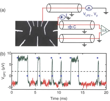
these measurements, we give an overview of the more important details of our mea-surement circuit and technique. A sketch of the circuit used for our meamea-surements is shown in Fig. 2-3(a). We amplify the voltage across the QPC with a Signal Recovery 5184 voltage preamplifier. This amplifier, which sits at room temperature near the top of the dilution refrigerator dewar, is connected to the QPC through a coaxial cable of capacitance C - 500 pF. When the QPC resistance Rqpc changes by a small amount, the voltage across the QPC Vc takes a time T = RqpcC ~ 50 ps to respond,
where here we have used a typical value for the QPC resistance Rqpc = 100 kQ. The
time intervals to,, and toff must be longer than r in order for them to be measurable. For all of the data reported here, we have used simulations to check that the finite bandwidth of our measurement does not substantially affect our results [43]. The few small effects that the finite measurement bandwidth has will be noted below. In Section 2.4 and in the following chapter, we quickly modulate the energy of the one
(a)
I -1=.. V+ V, -=(b)
100--5
0
5
10
15
20
Time (ms)
Figure 2-3: (a) Sketch of circuit used for performing time-resolve measurements of the charge on the quantum dot. A current I = 1 nA is sourced through the QPC resistance Rqpc and the voltage across the QPC Vqpq is amplified with a Signal Recovery 5184 voltage preamplifier. The bandwidth for this measurement is limited by the combination of the point contact resistance Rqpc and the capacitance C of the coaxial cable connecting the input of the preamplifier to the QPC, as discussed in the main text. To quickly modify the energy of the one electron state relative to the Fermi level, we add a small, high speed voltage V to the voltage applied to the gate LP2.
(b) Example of automated triggering software. Starting with a voltage vs. time series
such as the one shown in Fig. 2-2(c), we first determine where the data exceeds a specified threshold, shown here as a dashed black line, and retain data only in the immediate vicinity of where the threshold is exceeded (green sections of the time series). We then determine where the charge transitions from 0 to 1 (1 to 0) electrons are within these subsections of the data by determining where the derivative of the time series has a large positive (negative) value. We save only the times when the electron tunnels on and off the dot. These times are indicated by the blue circles: The upper value corresponds to an electron tunneling on, the lower value corresponds to an electron tunneling off.
electron state relative to the Fermi level. This is done by adding a small, high speed voltage V to the voltage applied to the gate LP2. V, can be varied on a microsecond time scale.
To measure the rates F,, and Foff accurately, we must measure many time in-tervals toff and t,,. For instance, for the histogram shown in Fig. 2-2(d), we have measured almost 10,000 time intervals. The time series shown in Fig. 2-2(c), which contains 10,000 data points, contains only 6 such time intervals. Therefore, the number of data points required for this measurement is approximately 20,000,000, re-quiring about 0.2 GB of memory. While performing one such measurement does not require too much memory, performing a large number of these measurements results in an unmanageable amount of data.
In order to reduce the amount of data acquired for our measurements, we devel-oped an automated triggering and acquisition system (Fig. 2-3(b)). For each time series that we acquire, our data is passed through a series of triggering algorithms before it is stored. The first algorithm determines when Vq4c exceeds a specified threshold. Only data close to where the threshold is exceeded are processed further (green regions in Fig. 2-3(b)). Following the threshold trigger, the data is passed through a second algorithm which finds the times at which Vqc jumps up or down suddenly. This is done by taking the derivative of the time series. Our derivative algorithm is modified so that it works properly for noisy data sets. We take the dif-ference between the average of two sets of data points separated by a specified delay time, and determine when this difference is sufficiently positive or negative, which tells us when an electron tunnels on or off the dot, respectively. The only data that we save are the time and type (tunneling on or off) of each of these charge transitions. Thus, the number of data points we actually save for a 10,000 point trace like the one shown in Fig. 2-3(b) is only 24. Our algorithms work fairly quickly so that the data acquisition time is not dominated by computation. In particular, the threshold trigger is implemented for the purpose of increased speed: It quickly cuts down on the amount of data that must be processed by the more time consuming differentiation algorithm. Our data acquisition system randomly saves a few voltage vs. time series
during the coarse of an experiment so that we can check that the triggering is working properly.
2.3
Energy Dependent Tunneling: Drain-Source
Bias Dependence
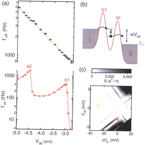
Using the charge sensing technique described in the previous section, we measure the rate for tunneling on F,, and off Foff the dot as a function of drain-source bias V
(Fig. 2-4(a)). These data are taken such that at V, = 0, the one electron state is just above the Fermi level in the leads. In the top panel of Fig. 2-4(a), we see that as V, is made more negative, F~ff increases exponentially.
To understand the exponential dependence of Loff on Vs, we start with the WKB formula [44) for an electron tunneling at an energy E through a potential barrier U(x):
=
foe-
f
2m*(U~x)-E)dx(2.3)
Here m* is the effective mass, fo can be regarded semiclassically as an attempt rate, and the integral in the exponent is taken over the classically forbidden region of length
w where U(x) > E. We linearize this formula for a small a perturbation 6E to the
electron energy E and a small deviation U of the tunnel barrier potential U(x):
r7
=Foe
K(6-E)(2.4)
Here t and Fo depend on the details of the barrier potential. For a quantum dot,
for small perturbations to the plunger gate voltage or drain-source bias 6V and 3Vd, about arbitrary but fixed V, and V values, the energy states on the (lot vary linearly as 6E = -eadsEVds - eagEV-q.4 Similarly, 6U varies linearly as U
=
-eCasdOVd, - eaguVq, where ad8U and agu give the coupling of V, and V to the
4Here, following the standard capacitor model for a quantum dot [38],
adsE is the ratio of the drain-source capacitance to the total dot capacitance, and likewise agE is the capacitance ratio for the three plunger gates.
barrier potential. There will, of course, be different parameters adsU, agu, K, and Fo for the two barriers b1 and b2. Note that F depends exponentially on U - 6E, and therefore depends exponentially on Vds and V: One can show that this holds independent of the particular shape U(x) of the barrier potential, or the shape of the perturbation to the potential induced by the change 6, or 6Vd,.
Using this linearization, we can write down equations for the V, dependence of Fff and F,,,, considering only the one electron ground state of the dot. We include the Fermi statistics in the leads by assuming that F,, (Foff) is the sum of two terms, proportional to the number of electrons (holes) in leads 1 and 2 at the ground state energy E. From the arguments given above, each term must also depend exponentially on Vd,, so that we obtain:
Foff F2,0e-32 Vds(1 -
f
2(E)) (2.5)+FI,oeSv(1 -
f
1(E))Fon = 7IF2,oC-2SVdf 2(E) (2.6)
+rlfi'oeCisvaWd fi (E)
Here /1,2 = hi,2|adsU - adsE|. The energy of the ground state relative to the Fermi level EF is given by E -eadEVd~ - eagEAVg, where AV is the shift in V from the
0 to 1 electron transition. f2 and fi are the Fermi distribution functions for the two
leads f2(E) = f(E), fi(E) =
f(E +
eVda), and 7) is the ratio between the tunnel rate onto and off of the dot for a given lead when the one-electron ground state is aligned with the Fermi level in that lead. We expect that r =- 2 because of spin degeneracy [24, 45], and use this value in the calculations below.To understand Fig. 2-4(a), we note that whether F increases or decreases with Vd depends on whether lead 1 is better coupled to the barrier or the dot, that is, whether adss or adsE is larger. Since b1 is closer to lead 1 than the dot, and b2 is farther from lead 1 than the dot, it follows that adsU > adsE > adsU2 (see Fig. 2-4(c)) [46]. Therefore, tunneling through bi (b2) increases (decreases) exponentially with increasing V. This is reflected in the signs of the exponentials appearing in Eqn.
(a)
7( 6. 5 . 4 b N 3 2b -e F1000
82e2
(C)
1000 0 0.025 0.050el
G (e / h) 4 5 2 N 100 C> 0 0 2.10
41 -5-5.0 -4.5 -4.0 -3.5 -3.0
-40 -20 0 20 Vds (mv) Avg (mv)Figure 2-4: (a). Fan and 17off as a function of Vd, for large negative Vds. The solid line in the upper panel is based on a theoretical fit to the data discussed in the main text. el and e2 indicate where the Fermi level in lead 1 is aligned with the 1st and 2nd orbitally excited states, respectively. (b) Sketch of the energy configuration of the quantum dot at the position el noted in the lower panel of (a). The solid blue line indicates the ground state of the quantum dot, and the dashed black line indicates the orbitally excited state el. After tunneling into the orbitally excited state e1, the electron quickly relaxes to the ground state (green arrow), as discussed in the main text. (c) Differential conductance vs. V, and V, showing the 0 to 1 electron transition. The tunnel rates for this case are made large enough so that the differential conductance can be measured using standard transport techniques. The data shown in (a) are taken at the position of the dashed line: At V, - 0, the 1 electron state is
close to the Fermi level in the leads. The zero and one electron Coulomb blockaded regions are noted.
... ...
2.5 and Eqn. 2.6.
The solid line through the the Foff data in Figure 5-4(a) is a fit to Eqn. 2.5, which for large negative bias reduces to F2,oe4
3
26Vds, since electrons only tunnel onto
the dot from lead 2. The rate F,, is shown as a function of j, in the lower panel of Fig 2-4(a). At the two points marked el and e2 in the figure FO. increases rapidly as the Fermi energy in lead 1 is aligned with an excited orbital state of the dot [47], as depicted in Fig. 2-4(b). The higher-energy orbital states are better coupled to the leads and thus Fo, rises rapidly when these states become available. From the positions of these rises and a measurement of adE, we find the energies of the 1st and 2nd excited orbital states to be 1.9 and 2.9 meV, respectively, above the ground state. These energies can also be measured, with larger tunneling rates through bi and b2, using standard transport techniques [20] (Fig. 2-4(c)), and the results are consistent.
We note that Foff does not show any special features at the points el and e2.6 This is because the electron decays rapidly out of the excited orbital states via emission of acoustic phonons [6, 48], and subsequently tunnels off the dot from the ground state [49]. We can therefore continue to use Eqn. 2.5 when there are multiple orbital states in the transport window.
In the regions between the points el and e2, F,, is seen to decrease exponentially as VS is made more negative, as expected from Eqn. 2.6. Note that this decrease in
FO,, with increasingly negative Va,, occurs even though the number of electrons that
could tunnel onto the dot inelastically from lead 1 is growing. This is strong evidence that the tunneling is predominantly elastic, dominated by states very close to the dot energy E. There is, however, an apparent flattening of FO,, above the extrapolated
5We will not discuss the standard model for Coulomb blockade diamonds as it is covered
ex-tensively elsewhere [20. 38]. From these diamonds, measured either with charge detection or with traditional transport techniques., one can measure agE and adsE.
'There is a very small kink in the Foff data at the position of e2. This is caused by the finite measurement bandwidth discussed in Section 2.2. When Fo, suddenly becomes very large. some time intervals tff will become too short to be ineasured. When a time interval toff is missed entirely., the two adjacent time intervals t,, are measured as a single interval, which has the effect of decreasing the measured rate loff relative to its actual value. We have performed simulations of this effect, and find that it accounts for the observed kink in the Ffof data.
exponential decrease near V =- -4 mV, close to the second excited orbital state. We
find that this line shape is consistent with broadening of the second excited state
by a Lorentzian of full-width at half-maximum ' ~ 10 peV. Calculated line shapes
are shown for the broadening of the first excited state in Fig. 2-5 and are discussed below.
If a square tunnel barrier is assumed, one can compute an effective barrier height
U2 and width w2 for b2 from the fit in Fig. 5-4(a). For a square barrier F
foe-2 /2m*(U 2-E)/h 2
[44]. Linearizing the square root in the exponential and esti-mating adsE - adU2 dsE and f0 ~ EQ/h ~ 1 THz, where EQ is the level spacing of the dot, we obtain w2 ~ 130 nm and U2 - EF ~ 5 meV at V1 , = V. These values are only logarithmically sensitive to fo and thus depend very little on our estimate of this parameter. If the barrier is assumed to be a different shape, for instance parabolic (as drawn in Fig. 2-4(b)), similar values are obtained (7 meV and 120 nm for the height and width of the barrier, respectively). The voltages we apply to the gates to create the tunnel barriers are the same order of magnitude as the voltages at which the 2DEG depletes and thus it is reasonable that U2 - EF is found to be comparable to the Fermi energy (EF ~ 7.7 meV). The value for W2 is also reasonable given the dimensions of our gate pattern and heterostructure.
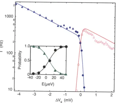
We next examine, in Fig. 2-5, the dependence of F,, and Foff on V, for both positive and negative Vd,. The data are taken with V adjusted so that E is kT
away from the 0 to 1 electron transition at V = 0. The solid blue and red lines in
Fig. 2-5 are calculated from Eqn. 2.5 and Eqn. 2.6 and are in good agreement with the data. Eqn. 2.5 agrees with the Foff for all V, while Eqn. 2.6 agrees with the F", data only for small Vd,. This is to be expected because Equations 2.5 and 2.6 only take into account the ground orbital state of the quantum dot. As shown above, the orbitally excited states into which electrons can tunnel when V, is made sufficiently positive or negative increase Fan but do not affect Fff. We note that the value of 01 is very close to the value of 02. If the height and width of b1 and b2 are comparable
one can show that
01
~ ldsUl (dsE #2, and it is therefore expected that 31 ~ 02.m
t
dsEl iedsU
2
1000
10
o"0
=
1000o0
1
0 100 0 O 0 E (peV) 100 =0 100on
1
I off
-2 0 2 VdS(mV)
Figure 2-5: Fon (closed squares) and lof (open circles) as a function of Vda. The solid red and blue curves are calculations of F, and foff that include only the contribution of the ground state to the tunneling as described in the main text. The dashed and solid green lines are calculations of Fo, including the contribution of one of the orbitally excited states to the tunneling for V, < 0 with and without Lorentzian broadening, as discussed in the main text. The step features near V, = 0 result from
the Fermi distribution. (Inset) Rate of tunneling into the ground state (open circles) and orbitally excited state el (closed squares) as a function of the energy E of the state relative to the Fermi level in the lead from which the electron is tunneling. The orbitally excited state data are taken from the drain-source bias dependence shown in the main part of this figure. The ground state data are taken by modulating the ground state energy relative to the Fermi level using the gate voltages as is discussed in the following section. The data are scaled vertically so that they agree for E < 0.
state el of the quantum dot from lead 1. In order to extend our model to account for this we add a term qriOeM13 'sfi(E
+
E1) to Eqn. 2.6. Here E1 is the energy of e1 relative to the ground state. Eqn. 2.6 with this addition is plotted as the solid green line in Fig. 2-5. We see that, for V slightly more positive than Vds -3 mV, whereel is just above the Fermi level in lead 1, the F0, data is substantially larger than the
solid green line. In order to account for this enhancement of F,, when el is just above the Fermi level, we included broadening of the state el by a Lorentzian of full-width at half-maximum -y 13 peV. This calculation is plotted as a dashed green line in
Eqn. 2.6, and agrees well with the data. fon also deviates from the solid curve for
Vd > 2 mV: This deviation may be caused by broadening of the first excited state as well. Though the lineshape including Lorentzian broadening of el agrees quite well with the data, it is not clear what this broadening could come from. Relaxation from el to the ground state via acoustic phonon emission leads to energy broadening of el. However, from the time-energy uncertainty principle, the energy broadening observed here corresponds to a lifetime of Tei = 50 ± 30 ps, and while emission of acoustic
phonons can lead to lifetimes ~ 100 ps, for our device parameters we expect much slower relaxation from this mechanism [6, 48, 50]. The tunneling process, which as shown above is much slower than the acoustic phonon relaxation, leads to a negligible amount of energy broadening. The enhancement of For, could alternatively be caused
by inelastic processes, which might begin to contribute significantly to F,,, when the
ground state of the dot is sufficiently far below the Fermi energy.
An obvious question with regards to this apparent broadening of the excited state el is whether the same broadening is observed for the ground state. As is shown in the inset to Fig. 2-5 the answer appears to be no. Using the data in the main plot, we plot Fo, as a function of the difference between the energy of el and the Fermi level in lead 1. In a separate experiment, we vary the energy E of the ground state relative to the Fermi level using the gates (as discussed in the following section), and we plot F,, vs. E for this data set in the inset at well. As the ground state is brought above the Fermi level, F17, drops exponentially over almost four orders of magnitude as the number of electrons in the leads at the energy of the ground state drops. In contrast,