Publisher’s version / Version de l'éditeur:
Laboratory Memorandum (Institute for Ocean Technology (Canada)), 2004
READ THESE TERMS AND CONDITIONS CAREFULLY BEFORE USING THIS WEBSITE. https://nrc-publications.canada.ca/eng/copyright
Vous avez des questions? Nous pouvons vous aider. Pour communiquer directement avec un auteur, consultez la
première page de la revue dans laquelle son article a été publié afin de trouver ses coordonnées. Si vous n’arrivez pas à les repérer, communiquez avec nous à [email protected].
Questions? Contact the NRC Publications Archive team at
[email protected]. If you wish to email the authors directly, please see the first page of the publication for their contact information.
Archives des publications du CNRC
For the publisher’s version, please access the DOI link below./ Pour consulter la version de l’éditeur, utilisez le lien DOI ci-dessous.
https://doi.org/10.4224/8895269
Access and use of this website and the material on it are subject to the Terms and Conditions set forth at
Integration of an isolation amplifier into an Aerotech Servo motor controller
Collett, C.
https://publications-cnrc.canada.ca/fra/droits
L’accès à ce site Web et l’utilisation de son contenu sont assujettis aux conditions présentées dans le site LISEZ CES CONDITIONS ATTENTIVEMENT AVANT D’UTILISER CE SITE WEB.
NRC Publications Record / Notice d'Archives des publications de CNRC:
https://nrc-publications.canada.ca/eng/view/object/?id=5536c589-14f3-474c-8038-83728b89bd1a https://publications-cnrc.canada.ca/fra/voir/objet/?id=5536c589-14f3-474c-8038-83728b89bd1a
Ocean Technology technologies oc ´eaniques
Laboratory Memorandum
LM-2004-28
Integration of an Isolation Amplifier into an Aerotech Servo
Motor Controller
C. Collett
August 2004
REPORT NUMBER
LM-2004-28
NRC REPORT NUMBER DATE
August 2004
REPORT SECURITY CLASSIFICATION
Unclassified
DISTRIBUTION
Unlimited
TITLE
Integration of an Isolation Amplifier into an Aerotech Servo Motor Controller AUTHOR(S)
Chad Collett
CORPORATE AUTHOR(S)/PERFORMING AGENCY(S)
National Research Council - Institute for Ocean Technology
PUBLICATION
SPONSORING AGENCY(S)
National Research Council - Institute for Ocean Technology
IMD PROJECT NUMBER NRC FILE NUMBER
KEY WORDS
Isolation Amplifier (Iso Amp)
PAGES 60 FIGS. 20 TABLES 18 SUMMARY
During this work-term I modified and fixed an existing isolation amplifier. As well I integrated it into an Aerotech motor controller package by rewiring the back panel. Then I proceeded to make a duplicate isolation amplifier so that it could be interchangeable with the first. Once complete I tested the system under a variety of conditions in different places to compare it to a second (unmodified) Aerotech motor controller package. In doing so I found many flaws with the testing setup and how it should be configured, which is included in the report.
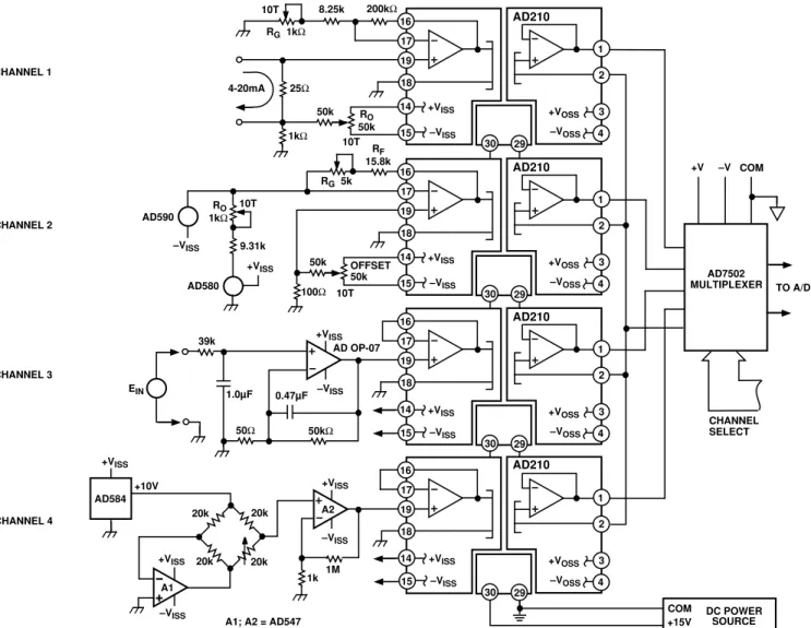
The reason to make an isolation amplifier is to eliminate “ground loop” noise in the analog rpm and current data, which is being derived from the motor controller system and recorded on the Data Collection System. By utilizing an Isolation Amplifier to interrupt the ground path, which occurs by connecting the Motor Controller analog output data directly to the Data Acquisition System ground loop, noise is eliminated. The isolation amplifier makes use of the AD210, a wide bandwidth 3 – port isolation amplifier. This chip uses transformer coupling to separate grounds. Therefore the data you receive is actually your true signal.
When modifying the isolation amplifier it helps to use the accompanying diagrams, schematics, and tables. In fact it is impossible to understand the circuit without them. When modifications are completed you can start the testing which is straightforward with the instructions. These tests just verify if the isolation amp is wired properly and acting the way it should. The next set of tests verifies that the motor controller system is operating correctly. The pictures and diagrams should be an aid to anyone setting up another data acquisition system as well.
ADDRESS National Research Council
Institute for Ocean Technology Arctic Avenue, P. O. Box 12093 St. John's, NL A1B 3T5
Institute for Ocean Institut des technologies
Technology océaniques
Integration of an Isolation Amplifier into
an Aerotech Servo Motor Controller
.
LM-2004-28
Chad Collett
Summary
During this work-term I modified and fixed an existing isolation amplifier. As well I integrated it into an Aerotech motor controller package by rewiring the back panel. Then I proceeded to make a duplicate isolation amplifier so that it could be interchangeable with the first. Once complete I tested the system under a variety of conditions in different places to compare it to a second (unmodified) Aerotech motor controller package. In doing so I found many flaws with the testing setup and how it should be configured, which is included in the report.
The reason to make an isolation amplifier is to eliminate “ground loop” noise in the analog rpm and current data, which is being derived from the motor controller system and recorded on the Data Collection System. By utilizing an Isolation Amplifier to interrupt the ground path, which occurs by connecting the Motor Controller analog output data directly to the Data Acquisition System ground loop, noise is eliminated. The isolation amplifier makes use of the AD210, a wide bandwidth 3 – port isolation amplifier. This chip uses transformer coupling to separate grounds. Therefore the data you receive is actually your true signal.
When modifying the isolation amplifier it helps to use the accompanying diagrams, schematics, and tables. In fact it is impossible to understand the circuit without them. When modifications are completed you can start the testing which is straightforward with the instructions. These tests just verify if the isolation amp is wired properly and acting the way it should. The next set of tests verifies that the motor controller system is operating correctly. The pictures and diagrams should be an aid to anyone setting up another data acquisition system as well.
According to the results, the system that I modified is almost as good as the original unmodified motor controller with an external isolation amplifier box attached. The difference in noise is in the 5 – 10 mV range, which is irrelevant when you are looking at a scale of 0 – 10 Volts. The little bit of extra noise seems to be coming from the
switching that is going on inside the motor controller package. So this project was a complete success in the fact that it frees up space in the testing environment. It also saves some time when trying to find equipment because you don’t have to go looking for another isolation amplifier to use with the system.
The integration of the isolation amplifier did not solve the noise problem with the system because the major noise is not coming from airborne radio frequencies. It is a
combination of the motor dynamometer, signal conditioner, AC power, transformer, and radio frequencies. These problems are minimized when you separate the system into two different groups, clean and dirty. Clean being the data acquisition side and dirty being the motor controller side. You can follow my instructions and pictures and see how this is accomplished.
Acknowledgements
Peter Hackett, designed the project and helped every step of the way. Jim Williams, gave pointers and help whenever I needed it.
Vaughan Benson, helped with the testing process and worked out problems. Tim Ennis, gave advice and helped set up the testing process.
Jody Farr, gave advice and was very helpful. Ed Kennedy, gave advice and tips.
Letter of Transmittal….………...1 Title Page……….. 2 Summary………... 3 Acknowledgements……….. 5 1.0 Introduction……….. 6 1.1 Background………..………... 6
1.2 Problems and Methodology……….………... 6
1.3 Scope………... 9
2.0 Noise and Analog Signals...……….………10
2.1 Definition of Noise………..……….………...10
2.2 Effects of Noise on Data Signals………..………...10
2.3 How to Decrease Noise in a Motor Controller.………..….11
3.0 Building or Modifying the System………..13
3.1 Making the Cables ………...13
3.2 Isolation Amplifier Circuit Boards.………..13
3.3 The Rear Panel………..14
4.0 Testing of the Isolation Amplifier………... 16
4.1 Materials.………..16
4.2 Pin Out Test…..………... 16
4.3 Power Test……….……….. 16
4.4 Functional Test of Unity Gain ……….17
5.0 Testing of the Motor Controller ……….19
5.1 Materials………...19
5.2 Setup……….19
5.3 Steps to Reduce Noise………..20
5.4 Steps to Set up the Signal Conditioner……….21
5.5 Steps for Data Collection………..22
6.1 Motor Controller One at 1500 RPM...…..………...…...……..26
6.2 Motor Controller Two at 1500 RPM...27
6.3 Motor Controller Three at 1500 RPM...28
6.4 Comparisons...29
7.0 Conclusion……….……30
7.0 Recommendations……….……31
References………. 32
Appendix A: Data Sheets AD210 Data Sheets……… 34
Power Supply Data Sheets………. 42
Appendix B: Tables, Drawings, and Schematics Isolation Amplifier Wiring Tables...45
Motor Controller/ Isolation Amplifier Box Schematic……….. 47
AD210 Layout, Pins, and Block Diagram...48
Calibration Tables...49
Block Diagram of Motor Controller Testing Setup...50
RF Filter Diagram...51
Appendix C: Photos……….………...52
Picture 1: Testing Setup In the Preparation Shop...53
Picture 2: Testing Setup, Bench 1...53
Picture 3: Testing Setup, Bench 2...53
Picture 4: Data collection with DaqView...54
Modified Motor Controller Package...55
Unmodified Rear Panel...56
Modified Rear Panel...56
Isolation Amplifier...57
Isolation Amplifier with Chips...57
Figure
1.1 External Isolations Amplifier...6
1.2 Internal Isolation Amplifier...6
1.3 Unmodified isolation amplified...7
1.4 Modified isolation amplifier...7
1.5 Proto board before rewiring...8
1.6 Proto board after rewiring...8
2.1 Effect of Noise on a Signal...10
2.2 AD210 Block Diagram...11
2.3 Velocity Signal Without Isolation...12
2.4 Velocity Signal After Isolation...12
3.1 Isolation Amplifier Top View...14
3.2 Rear Panel Layout...15
4.1 Modified Testing Cables...16
4.2 Modified Power Cable connected...17
4.3 Unity gain input and output signals...18
5.1 Normal operating conditions...20
5.2 Noise after PMM operating...20
5.3 Signals Conditioner Connected...22
5.4 Motor Controller Boards...24
1.0 Introduction 1.1 Background
The reason for this whole project is to improve an already existing Aerotech triple axis servo motor controller (I will refer to it as the motor controller). Previously the motor controller utilized an external eight-channel isolation amplifier, which was a mess. Refer to Figure 1.1.
Figure 1.1 External Isolations Amplifier Figure 1.2 Internal Isolation Amplifier
The idea was to integrate the isolation amplifier into the existing motor controller box as in Figure 1.2. This should have the following advantages:
- More portable
- Less wires hanging around to pick up noise and get in the way - More user friendly
- Protected from noise in the air by being inside of the motor controller
1.2 Problems and Methodology
A previous student created the aluminum boxes for the isolation amplifiers, populated the boards and wired it up. It was completed but did not operate correctly. Here are the problems and how they were fixed:
Problem 1:
When the motor controller was turned on it would go right to the rail meaning that it would reach top speed immediately. We tried many things to fix this, one of which was to put a 10 MΩ resistor across pins 18 and 19 on the command inputs at the AD210
amplifier. This should have caused no signal to go into the chips when no command is given, but didn’t work. When I was rewiring the chips I noticed that the output for each of the tachometer channels was on the wrong pin, pin 1 instead of 19. Tachometer is the signal from the motor telling the controller what speed it is going. Essentially the signal was reversed and told the motor to go faster when it was supposed to be idle.
Problem 2:
The original isolation amplifier box design had all of the incoming signal grounds tied together, which in turn defeated the isolation of the isolation amplifiers. So in order to fix this I brought in a separate wire for each of the incoming signals. To do this I had to replace the 10 pin bendix connector with a 19 pin to accommodate the extra wires. Then I had to rewire the rear panel of the motor controller. Figure 1.3 show the box before modification and Figure 1.4 shows it after.
Figure 1.3 Unmodified isolation amplified Figure 1.4 Modified isolation amplifier
Problem 3:
The grounds were still not isolated after each signal had its own ground. So in order to truly isolate the signals we have to implement a triple pole double throw switch. The
switch controls the command mode between command input BNC and remote hand held control potentiometer input. The hand held control potentiometer derives its excitation from a +/- 15 volt power supply within the motor controller which means the command isolation would be defeated if this signal were connected to the command isolation amplifier. The switch bypasses the isolation amplifier when switched to the hand held control potentiometer position. It allows only command input or remote input to work at once.
Problem 4:
There were some wiring problems that I found as I was testing and modifying the isolation amplifier circuitry. First to note is that the signal common and the power common were not connected properly across the chips. Also there were some wires crossing under chip sockets and a few other minor problems. Stripping all of the wires off the boards and rewiring everything fixed all of these problems. Figure 1.5 shows how the boards looked before and Figure 1.6 shows how it looks now.
1.2 Scope
This report discusses improvements and modifications to an existing triple axis motor controller with an internal isolation amplifier. Once created the system will have to be tested and compared to the unmodified version, which has an external isolation amplifier. After this the second motor controller will be modified to be the same as the first. This report will not cover the fabrication, and building of the isolation amplifier boxes or ordering of parts. Nathan Adams covered those topics in a previous report, Reducing Noise And Eliminating Ground loops in Triple Axis Servo Motor Controllers.
2.0 Noise and Analog Signals 2.1 Definition of Noise
Noise is any unwanted corruption to the normal signal. According to Omega Engineering “Noise can be categorized into two broad categories based on the source-internal noise and external noise. While internal noise is generated by components associated with the signal itself, external noise results when natural or man-made electrical or magnetic phenomena influence the signal as it is being transmitted.” Noise becomes a problem when you are trying to get an accurate reading of signal feedback.
2.2 Effects of Noise on Data Signals
When noise is present on a data signal there is no way to get an accurate reading of what the original signal was. Noise could be caused by sources such as fluorescent lights, radio frequencies, and air conditioning systems. Figure 2.1 shows the effects of noise on a data signal.
2.3 How to Decrease Noise in a Motor Controller
There are two ways of reducing noise on a data signal, one being to get rid of the device that is creating the external noise that is induced on your signal, the other is to use an isolation amplifier to clean up the signal before you read it. For our purposes we did both. The incorporation of the isolation amplifier into the motor controller will clean up the signals before they come out of the box. This is accomplished by using the AD210 chip, which is a 3-port isolation amplifier. In our case the isolation amplifier breaks the direct electrical connection between the motor controller signal ground and the data collection system signal ground and thus eliminates the potential for ground loop noise. The feature that provides this chip with such good isolation is transformer coupling. This occurs when two transformers are placed closely together so that the signal is passed from one transformer to the next. In order for a transformer to work there must be an AC waveform going into it. In figure 2.2 you can clearly see that at the output of the first op-amp there is a modulator that converts DC signals to AC signals.
This eliminates the DC noise in the signal. At the output of the second transformer there is a demodulator, which converts the signals back to DC. Figure 2.3 shows the signal before isolation and Figure 2.4 shows the signal after isolation.
Figure 2.3 Velocity Signal Without Isolation Figure 2.4 Velocity Signal After Isolation
After that you have to worry about external noise. We tried to move the motor controller testing setup around to achieve a less noisy setup in the prep shop; this is shown in Picture 1 in Appendix C. But there were air conditioners flowing and heavy machinery running which made it an overall noisy environment. In the end we found that we had to move the whole setup to the office area to reduce noise, see Pictures 2 and 3 in Appendix C. Section 5.2 outlines how to set up the isolation amplifier for noise reduction.
3.0 Building or Modifying the System
This section will explain the process to go about when building or modifying an isolation amplifier for use the Aerotech triple axis motor controller. You will need to utilize the motor controller schematic, isolation amplifier wiring tables, and AD210 layout, pin designation, and block diagram in Appendix B in order to understand how everything is interconnected. For information specific to the AD210 and how it works, refer to the data sheets in Appendix A.
3.1 Making the Cables
When making the cables for the internal connections for the isolation amplifier make sure to reference the tables and diagrams of Appendix B. Use the color coding which is used in the wiring table for each connector. This ensures uniformity among components and reduces the risk of error when soldering. The first thing to do is solder the wires to their pins on the appropriate bendix connector. The Pana Vise can be used to make this job easier by clamping it on the connector head. Make sure that you put the full assembly (strain relief clamp, bushing, and rubber insulator) on the cable before you begin
soldering. When you have the cables made then you can begin to make connections to the Isolation Amplifier.
3.2 Isolation Amplifier Circuit Boards
Referring to the wiring table, AD210 diagrams, and schematic in Appendix B, the isolation amplifier circuit boards can be wired. It looks to be a hard task at first, but it is quite simple after some examination of tables and diagrams. If you refer to figure 3.1 you can see the layout of the top board.
Figure 3.1 Isolation Amplifier Top View
Do not attach the cables to the box yet because you need room to work. Place the circuit boards and power supply in the box before hand to ensure proper length for the wires. Snip the wires when you have the correct length. Solder them into their correct places and when all of the wires are connected, use small wires to act as tie wraps to hold the
interconnect wiring to the circuit board.
3.3 The Motor Controller Package Rear Panel
The rear panel is where everything goes in and out of the motor controller. So there are many wires running from the rear panel to the isolation amplifier and motor controller. This can be seen in Figure 3.2.
Figure 3.2 Rear Panel Layout
The wiring of the rear panel can be done in the same way as the isolation amplifier. You can use the schematic and the wiring tables to complete the job. Once everything is wired up and you are confident it works, then it is time to begin testing.
4.0 Testing of Isolation Amplifier
4.1 Materials - Isolation Amplifier - Oscilloscope
- Universal Source or Function Generator - Digital Multimeter
- 3 BNC to BNC connectors
- Testing Cables Figure 4.1 Modified Testing Cables
- Modified power cable (2 pin to plugin)
- 37 pin female connector to stripped wires
4.2 Pin Out Test
The function of this test is to ensure that connections are made correctly to specific points on each board and to the correct places on the rear panel. For this test you should use the isolation amplifier wiring diagram and schematic, which are located in appendix B. You will use the ohm’s function on the DMM (digital multi-meter) to put one lead on the pin of the external connector and another lead on its appropriate point on the board.
Afterwards make sure that there is no continuity between the power pins and any other pin. Then verify that the signal common is actually common between all of the chips.
4.3 Power Test
This test is just to see if power is flowing where it should or shouldn’t be. Remove all AD210 chips from the circuit. (Make sure not to bend pins on the chips, they are very fragile. Plug the modified power cable into the power input of the isolation amplifier, like
in Figure 4.2. Use a multimeter to verify with the DC voltage function that there is 15 Vdc between pins 29 and 30 on each chip circuit. Then make sure there is no voltage between 29 and any other pin, and 30 and any other pin.
Figure 4.2 Modified Power Cable connected
4.4 Functional Test of Unity Gain
The following test is to check the unity gain of each of the AD210’s (what goes in should come out). To perform this test all of the AD210’s have to be placed in their
corresponding positions. Put the cover back on the Isolation amp and then put it into the motor controller case. You are going to use the rear panel of the motor controller to perform the following test. Follow these steps:
1) Connect the modified power cable, the isolated rear panel cable, and the Motor controller cable to the Iso Amp.
2) Connect the 37 pin female end of the testing cable to the male end of the motor controller cable.
3) Connect a BNC T connector to the output of the universal source.
4) Then connect a BNC cable from the T connector to the oscilloscope and another one from the T connector to the command input on the rear panel.
5) Then connect a BNC cable to the oscilloscope and some alligator clips to the opposite end.
6) Connect the alligator clips to the motor controller output cable. Black to the black wire, red to the wire you are testing, in this case purple or CMD1.
7) Now on the oscilloscope line up channel 1 on the 2nd line from the top, and channel 2 on the 2nd line from the bottom, making sure that their amplitudes are the same. For our purposes 2 V/div should be sufficient.
8) Place the command input mode switch (triple pole double throw) in the “command BNC” position.
9) Now turn on the source let it warm up for approximately 10 minutes and set it for 5 V(peak) at 10 Hz. The waveforms on the oscilloscope should be exactly the same, see Figure 4.3.
Figure 4.3 Unity gain input and output signals
Do the same for the other 2 command inputs. Inputting the signal through command and receiving it on the motor controller cable. For the Tach and Current you have to do exactly the opposite. Just switch around the cable on the BNC T connector and oscilloscope so that you have input going in through the motor controller and output coming out on the rear panel. These signals should also be exactly the same as well.
5.0 Testing of Motor Controller 5.1 Materials
- Signal conditioner with output signal buffer installed, signal conditioner power supply, and appropriate power supply output cable
- Signal conditioner analog output cable to daqboard /2000
- DASPC (#14 preferably), monitor, keyboard, mouse, Daqboard /2000 ribbon cable and DBK 201 interconnect board
- Marine UPS
- Dual output DC power supply for command signal derivation - 2 digital multimeter
- Motor Controller Package - Power transformer
- Motor Dynamometer - Emergency stop for enable - Hand held optical Tachometer
- 2 BNC – 10 pin bendix cables for connection of motor controller isolated output signals to Signal Conditioner
- 2 of 1Khz passive Low Pass filters to reduce RF rectification level shift effects on the isolated data
- 4 to 8 BNC cables, BNC to banana clips, T connectors, etc.
5.2 Setup
The first thing to do when starting the testing process is to set up each component in the correct position to achieve maximum noise reduction. Pictures 2 and 3 in Appendix C
show how I achieved this. Of the many configurations that were tested this proved to be the best scenario. . The setup block diagram in Appendix B shows where each device interconnects.
5.3 Steps to reduce noise
1 - The first thing to take note of is where you have the separate devices plugged in. Make sure that the power transformer is on a separate power grid from the meters, and UPS.
2 - The transformer should also be located as far away from the testing setup as possible so that the Switching RF noise is not radiated onto the monitoring cables.
3 - The next thing to do is make sure there are no major noise producers running in the vicinity, and especially not on the same power grid. In the case of the Model Prep Shop test area this could include the PMM, or any other motor.
Figure 5.1 Normal operating conditions Figure 5.2 Noise after PMM operating
4 - After that the computer, monitor, and the signal conditioner should be plugged into the UPS.
5 - Next plug 4 grounding plugs into the signal conditioner on the 4 adjacent connections from the active measuring channels, CH 00 and 02, on the signal conditioner input. These are 01, 03, 14, and 15. This reduces cross talk produced by the signal
6 – Finally, inline 1 Khz passive low pass filters have to be placed at the CH 00 and 02 inputs to the signal conditioner. The purpose of these filters is to reduce the effect of data level shift which is produced by RF rectification within each Signal Conditioner instrumentation amplifier channel. The designs for the 1Khz RF filters can be located in Appendix B.
Once everything is connected according to the diagram then you can begin collecting data. Prior to starting you should make sure that the motors are spinning in the right directions. Enable the driving motor and apply a command voltage from the left channel of the Dual power supply noting which direction it is going. To determine direction you look into the motor from the shaft. If it is spinning clockwise then it is considered positive. Then disable the driving motor and turn up the command voltage (right channel of the Dual Power Supply) for the current control motor (brake motor) and note the direction of rotation. This motor should be spinning in opposite direction
because you are using the current motor as a brake for the driving motor.
5.4 Steps to set up the Signal Conditioner
When you get a signal conditioner, there are many things to take into consideration before using it. Ask someone in the lab to help you get an Un-buffered signal conditioner. Separate the used channels with grounding plugs and place one before and after to
Figure 5.3 Signals Conditioner Connected
Take the back off the signal conditioner and configure it to the following settings for the inputs used:
- Set the gain of the isolated tach feedback channel (CH 00) to 2 and the gain of the isolated current feedback channel (CH 02) to 4.
- Set the filters to 10 Hz.
- Make sure both channels are configured for 10V “local” excitation mode. - Attenuation Jumper set to “No Atten” for both channels.
When configured, place a grounding plug into the used inputs and then adjust the offset potentiometer on the front of the signal conditioner to obtain zero volts output on the corresponding channel. This removes the inherent offset on the active data channels.
5.5 Steps for Data Collection
1 - Load up daqview and load the configuration called Chad's test.DAQ from the CD, which has all of my motor controller testing on it. If you can’t find the file then you
can configure the settings yourself. The sampling rate is 50 Hz, set the start and stop triggers to manual, set the data collection to ASCII and Binary.
2 - Label the collection file to something recognizable. I used the following format: mod_1_cmd_300_amp2. Which translates into: modified controller, motor 1, command input, 300 RPM, isolation amplifier #2.
3 - Place the clock and daqview up on the screen as in Picture 4.
4 - Set the velocity command voltage to its corresponding RPM value according to the calibration tables located in Appendix B. You can verify the RPM value with the handheld tachometer.
5 – For 300 RPM motor speed, set the current command voltage until a reading of plus or minus 0.5V (depending on direction) on the DMM is reached. This corresponds to approx. 2.5 amps of current being drawn by the driving motor. Note that for the 1200 and 1500 RPM test speeds the DMM voltage will already be more than 0.5V due to the current required to produce the commanded speed and overcome the torque load produced by the brake motor at a 0 volt current command signal.
6 - Unplug the UPS from the wall. This gives clean power to the DASPC. 7 - Press the acquire data button (has coins on it). Then press the manual trigger button when the clock arm is on a dot on the clock. Time it for 30 seconds, then change the current command to produce a 1.0V level on the DMM. This corresponds to 5 amps of current being drawn by the driving motor. After 30 seconds change current input to 1.8V that corresponds to 9 amps of current being drawn by the driving motor. Wait another 30 seconds and then stop the data collection.
9 - Start again from step 2 and acquire data for 1200 and 1500 RPM speeds. 10. Switch the drive motor and command and feedback connections to controller 2 and repeat steps 2 through 8.
When you get to the third motor controller, you have to switch the personality chips on the front panel of the motor controller. Motor three is working in current mode and we need to have it working in normal mode in order to test it. So just take out motor controller 1 and 3 as in Figure 5.4 being careful not to interchange.
Figure 5.4 Motor Controller Boards
Then remove the personality modules, see Figure 5.5. Swap them around and then put the motor controllers back where they were before. If you don’t remember what order they were in, motor 1 is on the left.
Figure 5.5 Personality Modules
Once done the testing with command BNC inputs, it is time to start using the hand held remote control boxes to control the motors. The steps above can be followed, just make changes where you need to.
5.6 Steps to using Excel
1 – When you first open excel there are 3 tabs at the bottom of the page for different spreadsheets. You should use them to put different tests on different tabs. In this
way it makes it easy to compare from test to test. Go to the Data, Get External Data, Import text file and select the ASCII text file for the test you want. The ASCII files will be wherever you chose to save them.
2 – Right click on the data you have just imported and go to the number tab, then select general.
3 – Press the Chart Wizard button then the custom types tab and then select lines on 2 axis.
4 – Pick a size to drag your chart and use the gridlines to make them the same Amplitude scaling each time for easy comparison.
5 – Double click on each line type and turn the markers to none.
6 – Change the markers on the x-axis to none so that no marks are visible. 7 – Change the Y-axis scales so that each test has the same scale and is therefore comparable.
8 – Right click on the data and click on edit text import, copy the name of the file and then paste the name into the tab for the spreadsheet.
6.0 Results and Comparisons
This is what all of the work comes down to, seeing which motor controller produces the least amount of noise. For each of these tables the data was imported into excel for easy comparisons using the process discussed in section 5.6. RPM are in purple and use the left axis and Current is in blue and uses the right axis.
6.1 Motor Controller 1 at 1500 RPM 9.2 9.3 9.4 9.5 9.6 -8 -6 -4 -2 0 9.2 9.3 9.4 9.5 9.6 -8 -6 -4 -2 0
Unmodified, Unisolated Unmodfied, Isolated
9.2 9.3 9.4 9.5 9.6 -8 -7 -6 -5 -4 -3 -2 -1 0 9.2 9.3 9.4 9.5 9.6 -8 -6 -4 -2 0
9.2 9.3 9.4 9.5 9.6 -8 -7 -6 -5 -4 -3 -2 -1 0 9.2 9.3 9.4 9.5 9.6 -8 -6 -4 -2 0
Modified, Command, Isolation Amplifier 2 Modified, Remote, Isolation Amplifier 2
6.2 Motor Controller 2 at 1500 RPM -9.7 -9.65 -9.6 -9.55 -9.5 -9.45 -9.4 -9.35 -9.3 0 1 2 3 4 5 6 7 8 -9.7 -9.65 -9.6 -9.55 -9.5 -9.45 -9.4 -9.35 -9.3 0 1 2 3 4 5 6 7 8
Unmodified, Unisolated Unmodified, External Isolation
-9.7 -9.6 -9.5 -9.4 -9.3 0 2 4 6 8 -9.7 -9.65 -9.6 -9.55 -9.5 -9.45 -9.4 -9.35 -9.3 0 1 2 3 4 5 6 7 8
-9.7 -9.6 -9.5 -9.4 -9.3 0 2 4 6 8 -9.7 -9.65 -9.6 -9.55 -9.5 -9.45 -9.4 -9.35 -9.3 0 1 2 3 4 5 6 7 8
Modified, Command, Isolation Amplifier 2 Modified, Remote, Isolation Amplifier 2
6.3 Motor Controller 3 at 1500 RPM 9.45 9.55 9.65 9.75 9.85 -8 -6 -4 -2 0 9.45 9.55 9.65 9.75 9.85 -8 -7 -6 -5 -4 -3 -2 -1 0
Unmodified, Unisolated Unmodified, External Isolation
9.45 9.55 9.65 9.75 9.85 -8 -6 -4 -2 0 9.45 9.55 9.65 9.75 9.85 -8 -6 -4 -2 0
9.45 9.55 9.65 9.75 9.85 -8 -7 -6 -5 -4 -3 -2 -1 0 9.45 9.55 9.65 9.75 9.85 -8 -6 -4 -2 0
Modified, Command, Isolation Amplifier 2 Modified, Command, Isolation Amplifier 2
6.4 Comparisons
I tested the motor controllers under a variety of conditions. Unmodified, internally isolated, and externally isolated at +/- 300, 1200, and 1500 RPM. As well remote controlled, and with the two different isolation amplifiers that I made. I chose to only show the 1500 RPM results because each set shows the same results. From the results above it can be seen that the un-isolated motor controller has much more noise riding on the signals. This is true for each case. You can also see that the externally isolated motor controller has less noise that the internal one. But this noise difference is minimal
because the scale of the reading is so small. You can also see that isolation amplifiers 1 and 2 are identical in their readings, and they should be. Except on motor 3 where you can clearly see that there are larger spikes of noise on isolation amplifier 2. This could be due to some noise in the testing area at the time of testing.
7.0 Conclusion
According to the results the system that I modified is almost as good as the original with external isolation. The difference in noise is in the 5 – 10 mV range, which is irrelevant when you are looking at a scale of 0 – 10 Volts. The little bit of extra noise seems to be coming from the switching that is going on inside the motor controller. Both the internal and externally isolated motor controllers out-perform the un-isolated version. The separate setups react differently in unlike environments. Because being inside the box protects it from airborne noise, the internally isolated motor controller works better in more noisy environments. You can also see from the results that as you increase load on the motor the noise also increases. This is because the motor has to work harder. From these findings the integration of the isolation amplifier into the Aerotech triple axis servo motor controller was a success.
I have put a lot of time and energy into modifying, testing and documenting the motor controller. I feel confident that this document is sufficient enough for a technologist to use if they were to modify or build an isolation amplifier. This project has helped build confidence in my field of study and has given me experience to carry into my future career.
8.0 Recommendations
The integration of the isolation amplifier did not solve the noise problem with the system because the major noise is not coming from airborne radio frequencies. It is a
combination of the motor dynamometer, signal conditioner, AC power, transformer, and radio frequencies. All of this noise happens when the signals exit the motor controller box. If you were to really get rid of the noise there are larger problems to tackle. One such problem being the signal conditioners, they are a prevalent source of noise, cross talk, and other problems. Another problem is the proximity of the motor controller to the power transformer and it being on the same power grid. Also if the motor dynamometer is off balance, it will create noise. These problems are simplified when you separate the system into two different groups, clean and dirty. Clean being the data acquisition side and dirty being the motor controller side. You can follow my instructions and pictures you can see how this is accomplished. I hope that my outline for testing the motor controller solves a few problems in the future when setting up the data collection systems.
There is the issue of the remaining isolation amplifier box that I have made. It works perfect but due to time constraints I will not have time to integrate it into the other motor controller. If the next IOT student/employee wants to integrate it then the instructions I have made should work fine. It was mentioned to me that the chips inside could be used in a more cost efficient way by making a couple more external four-channel isolation amplifiers. As each AD210 costs approximately $200 then this would make a lot of sense. Whatever the case this document will be of help in doing the task.
References
Adams, Nathanael (2002). Reducing Noise And Eliminating Ground loops in Triple Axis Servo Motor Controllers. St. John’s: Institute for Ocean Technology at the National Research Council.
[Anonymous] Analog Devices AD210 Data Sheets (2004); Available from:
http://www.analog.com/UploadedFiles/Data_Sheets/713828300ad210.pdf via the Internet. Accessed June 12, 2004.
Areotech, INC. (1990). Operator’s Manual for the DS16030 Series Servo Amplifiers and DSR/DSRF Mounting Racks. Kitchener: Optikon Corporation Ltd.
Omega Engineering, INC. Analog Signal Transmission: Noise and Grounding (2004); Avaliable from: http://www.omega.com/literature/transactions/volume2/
Appendix A:
Data Sheets
One Technology Way, P.O. Box 9106, Norwood, MA 02062-9106, U.S.A.
Tel: 617/329-4700 Fax: 617/326-8703
FUNCTIONAL BLOCK DIAGRAM
INPUT POWER SUPPLY 19 14 15 16 17 18 VO 30 29 T2 POWER POWER OSCILLATOR INPUT OUTPUT MOD DEMOD FILTER 1 2 OUTPUT POWER SUPPLY 3 4 OCOM +VOSS –VOSS AD210 PWR COM PWR T3 T1 –VISS +VISS ICOM +IN –IN FB
a
3-Port Isolation Amplifier
AD210*
FEATURES
High CMV Isolation: 2500 V rms Continuous
63500 V Peak Continuous
Small Size: 1.00" 3 2.10" 3 0.350"
Three-Port Isolation: Input, Output, and Power Low Nonlinearity: 60.012% max
Wide Bandwidth: 20 kHz Full-Power (–3 dB) Low Gain Drift: 625 ppm/8C max
High CMR: 120 dB (G = 100 V/V) Isolated Power: 615 V @ 65 mA Uncommitted Input Amplifier APPLICATIONS
Multichannel Data Acquisition
High Voltage Instrumentation Amplifier Current Shunt Measurements
Process Signal Isolation GENERAL DESCRIPTION
The AD210 is the latest member of a new generation of low cost, high performance isolation amplifiers. This three-port, wide bandwidth isolation amplifier is manufactured with sur-face-mounted components in an automated assembly process. The AD210 combines design expertise with state-of-the-art manufacturing technology to produce an extremely compact and economical isolator whose performance and abundant user features far exceed those offered in more expensive devices. The AD210 provides a complete isolation function with both signal and power isolation supplied via transformer coupling in-ternal to the module. The AD210’s functionally complete de-sign, powered by a single +15 V supply, eliminates the need for an external DC/DC converter, unlike optically coupled isolation devices. The true three-port design structure permits the AD210 to be applied as an input or output isolator, in single or multichannel applications. The AD210 will maintain its high performance under sustained common-mode stress.
Providing high accuracy and complete galvanic isolation, the AD210 interrupts ground loops and leakage paths, and rejects common-mode voltage and noise that may other vise degrade measurement accuracy. In addition, the AD210 provides pro-tection from fault conditions that may cause damage to other sections of a measurement system.
PRODUCT HIGHLIGHTS
The AD210 is a full-featured isolator providing numerous user benefits including:
High Common-Mode Performance: The AD210 provides 2500 V rms (Continuous) and ±3500 V peak (Continuous)
common-mode voltage isolation between any two ports. Low input capacitance of 5 pF results in a 120 dB CMR at a gain of 100, and a low leakage current (2 µA rms max @ 240 V rms, 60 Hz). High Accuracy: With maximum nonlinearity of ±0.012% (B Grade), gain drift of ±25 ppm/°C max and input offset drift of (±10 ±30/G) µV/°C, the AD210 assures signal integrity while providing high level isolation.
Wide Bandwidth: The AD210’s full-power bandwidth of 20 kHz makes it useful for wideband signals. It is also effective in applications like control loops, where limited bandwidth could result in instability.
Small Size: The AD210 provides a complete isolation function in a small DIP package just 1.00" × 2.10" × 0.350". The low profile DIP package allows application in 0.5" card racks and assemblies. The pinout is optimized to facilitate board layout while maintaining isolation spacing between ports.
Three-Port Design: The AD210’s three-port design structure allows each port (Input, Output, and Power) to remain inde-pendent. This three-port design permits the AD210 to be used as an input or output isolator. It also provides additional system protection should a fault occur in the power source.
Isolated Power: ±15 V @ 5 mA is available at the input and output sections of the isolator. This feature permits the AD210 to excite floating signal conditioners, front-end amplifiers and remote transducers at the input as well as other circuitry at the output.
Flexible Input: An uncommitted operational amplifier is pro-vided at the input. This amplifier provides buffering and gain as required and facilitates many alternative input functions as required by the user.
Information furnished by Analog Devices is believed to be accurate and reliable. However, no responsibility is assumed by Analog Devices for its use, nor for any infringements of patents or other rights of third parties which may result from its use. No license is granted by implication or otherwise under any patent or patent rights of Analog Devices.
REV. A
AD210 PIN DESIGNATIONS
Pin Designation Function
1 VO Output
2 OCOM Output Common
3 +VOSS +Isolated Power @ Output
4 –VOSS –Isolated Power @ Output
14 +VISS +Isolated Power @ Input
15 –VISS –Isolated Power @ Input
16 FB Input Feedback
17 –IN –Input
18 ICOM Input Common
19 +IN +Input
29 Pwr Com Power Common
30 Pwr Power Input
Model AD210AN AD210BN AD210JN
GAIN
Range 1 V/V – 100 V/V * *
Error ±2% max ±1% max *
vs. Temperature(0°C to +70°C) +25 ppm/°C max * * (–25°C to +85°C) ±50 ppm/°C max * *
vs. Supply Voltage ±0.002%/V * *
Nonlinearity1 ±0.025% max ±0.012% max *
INPUT VOLTAGE RATINGS
Linear Differential Range ±10 V * *
Maximum Safe Differential Input ±15 V * *
Max. CMV Input-to-Output *
ac, 60 Hz, Continuous 2500 V rms * 1500 V rms
dc, Continuous ±3500 V peak * ±2000 V peak
Common-Mode Rejection *
60 Hz, G = 100 V/V *
RS ≤ 500 Ω Impedance Imbalance 120 dB * *
Leakage Current Input-to-Output *
@ 240 V rms, 60 Hz 2µA rms max * *
INPUT IMPEDANCE
Differential l012Ω * *
Common Mode 5 GΩi5 pF * *
INPUT BIAS CURRENT
Initial, @ +25°C 30 pA typ (400 pA max) * *
vs. Temperature (0°C to +70°C) 10 nA max * *
(–25°C to +85°C) 30 nA max * *
INPUT DIFFERENCE CURRENT
Initial, @ +25°C 5 pA typ (200 pA max) * *
vs. Temperature(0°C to + 70°C) 2 nA max * * (–25°C to +85°C) 10 nA max * * INPUT NOISE Voltage (l kHz) 18 nV/√Hz * * (10 Hz to 10 kHz) 4µV rms * * Current (1 kHz) 0.01 pA/√Hz * * FREQUENCY RESPONSE Bandwidth (–3 dB) * G = 1 V/V 20 kHz * * G = 100 V/V 15 kHz * *
Settling Time (±10 mV, 20 V Step) *
G = 1 V/V 150 µs * *
G = 100 V/V 500 µs * *
Slew Rate (G = 1 V/V) 1 V/µs * *
OFFSET VOLTAGE (RTI)2
Initial, @ +25°C ±15 ±45/G) mV max (±5 ±15/G) mV max * vs. Temperature (0°C to +70°C) (±10 ±30/G) µV/°C * * (–25°C to +85°C) (±10 ±50/G) µV/°C * * RATED OUTPUT3
Voltage, 2 kΩ Load ±10 V min * *
Impedance 1 Ω max * *
Ripple (Bandwidth = 100 kHz) 10 mV p-p max * *
ISOLATED POWER OUTPUTS4
Voltage, No Load ±15 V * *
Accuracy ±10% * *
Current ±5 mA * *
Regulation, No Load to Full Load See Text * *
Ripple See Text * *
POWER SUPPLY
Voltage, Rated Performance +15 V dc ± 5% * *
Voltage, Operating +15 V dc ± 10% * *
Current, Quiescent 50 mA * *
Current, Full Load – Full Signal 80 mA * *
TEMPERATURE RANGE Rated Performance –25°C to +85°C * * Operating –40°C to +85°C * * Storage –40°C to +85°C * * PACKAGE DIMENSIONS Inches 1.00 × 2.10 × 0.350 * * Millimeters 25.4 × 53.3 × 8.9 * * NOTES
*Specifications same as AD210AN.
1Nonlinearity is specified as a % deviation from a best straight line.. 2RTI – Referred to Input.
3A reduced signal swing is recommended when both ±V
ISS and ±VOSS supplies are fully
loaded, due to supplyvoltage reduction.
4See text for detailed information. _
Specifications subject to change without notice.
REV. A –2–
OUTLINE DIMENSIONS
Dimensions shown in inches and (mm).
AC1059 MATING SOCKET
CAUTION
ESD (electrostatic discharge) sensitive device. Elec-trostatic charges as high as 4000 V readily accumu-late on the human body and test equipment and can discharge without detection. Although the AD210 features proprietary ESD protection circuitry, per-manent damage may occur on devices subjected to high energy electrostatic discharges. Therefore, proper ESD precautions are recommended to avoid performance degradation or loss of functionality.
WARNING!
REV. A –3– INSIDE THE AD210
The AD210 basic block diagram is illustrated in Figure 1. A +15 V supply is connected to the power port, and
±15 V isolated power is supplied to both the input and output ports via a 50 kHz carrier frequency. The uncom-mitted input amplifier can be used to supply gain or buff-ering of input signals to the AD210. The fullwave modulator translates the signal to the carrier frequency for application to transformer T1. The synchronous demodu-lator in the output port reconstructs the input signal. A 20 kHz, three-pole filter is employed to minimize output noise and ripple. Finally, an output buffer provides a low impedance output capable of driving a 2 kΩ load.
INPUT POWER SUPPLY 19 14 15 16 17 18 VO 30 29 T2 POWER POWER OSCILLATOR INPUT OUTPUT MOD DEMOD FILTER 1 2 OUTPUT POWER SUPPLY 3 4 OCOM +VOSS –VOSS AD210 PWR COM PWR T3 T1 –VISS +VISS ICOM +IN –IN FB
Figure 1. AD210 Block Diagram
USING THE AD210
The AD210 is very simple to apply in a wide range of ap-plications. Powered by a single +15 V power supply, the AD210 will provide outstanding performance when used as an input or output isolator, in single and multichannel configurations.
Input Configurations: The basic unity gain configura-tion for signals up to ±10 V is shown in Figure 2. Addi-tional input amplifier variations are shown in the following figures. For smaller signal levels Figure 3 shows how to obtain gain while maintaining a very high input impedance.
19 14 15 16 17 18 VOUT (±10V) 30 29 +VOSS VSIG ±10V AD210 +VISS –VISS +15V 2 3 4 –VOSS 1 VOUT
Figure 2. Basic Unity Gain Configuration
The high input impedance of the circuits in Figures 2 and 3 can be maintained in an inverting application. Since the AD210 is a three-port isolator, either the input leads or the output leads may be interchanged to create the signal inversion. 19 14 15 16 17 18 30 29 +VOSS VSIG AD210 +VISS –VISS +15V 2 3 4 –VOSS 1 VOUT = VSIG ( )1+ RF RG RG RF
Figure 3. Input Configuration for G > 1
Figure 4 shows how to accommodate current inputs or sum cur-rents or voltages. This circuit configuration can also be used for signals greater than ±10 V. For example, a ±100 V input span can be handled with RF = 20 kΩ and RS1 = 200 kΩ.
19 14 15 16 17 18 30 29 +VOSS AD210 +VISS –VISS +15V 2 3 4 –VOSS 1 RS1 IS VS2 VS1 RS2 RF VOUT VOUT = –RF VS1 RS1 ( )VS2 RS2 + + IS + ...
Figure 4. Summing or Current Input Configuration
Adjustments
When gain and offset adjustments are required, the actual cir-cuit adjustment components will depend on the choice of input configuration and whether the adjustments are to be made at the isolator’s input or output. Adjustments on the output side might be used when potentiometers on the input side would represent a hazard due to the presence of high common-mode voltage during adjustment. Offset adjustments are best done at the input side, as it is better to null the offset ahead of the gain. Figure 5 shows the input adjustment circuit for use when the in-put amplifier is configured in the noninverting mode. This offset adjustment circuit injects a small voltage in series with the
19 15 16 17 18 30 29 +VOSS AD210 +VISS –VISS +15V 2 3 4 –VOSS RG HI VOUT VSIG 14 200Ω 47.5kΩ 5kΩ 100kΩ 50kΩ LO GAIN OFFSET 1
REV. A –4–
low side of the signal source. This will not work if the source has another current path to input common or if current flows in the signal source LO lead. To minimize CMR degradation, keep the resistor in series with the input LO below a few hundred ohms. Figure 5 also shows the preferred gain adjustment circuit. The circuit shows RF of 50 kΩ, and will work for gains of ten or
greater. The adjustment becomes less effective at lower gains (its effect is halved at G = 2) so that the pot will have to be a larger fraction of the total RF at low gain. At G = 1 (follower)
the gain cannot be adjusted downward without compromising input impedance; it is better to adjust gain at the signal source or after the output.
Figure 6 shows the input adjustment circuit for use when the input amplifier is configured in the inverting mode. The offset adjustment nulls the voltage at the summing node. This is pref-erable to current injection because it is less affected by subse-quent gain adjustment. Gain adjustment is made in the feedback and will work for gains from 1 V/V to 100 V/V.
19 15 16 17 18 30 29 +VOSS AD210 +VISS –VISS +15V 2 3 4 –VOSS VOUT VSIG 14 200Ω 47.5kΩ 5kΩ 100kΩ GAIN OFFSET 50kΩ RS 1
Figure 6. Adjustments for Inverting Input
Figure 7 shows how offset adjustments can be made at the out-put, by offsetting the floating output port. In this circuit, ±15 V would be supplied by a separate source. The AD210’s output amplifier is fixed at unity, therefore, output gain must be made in a subsequent stage. 19 15 16 17 18 30 29 +VOSS AD210 +VISS –VISS +15V 2 3 4 –VOSS VOUT 14 200Ω 1 0.1µF 100k OFFSET 50kΩ +15V –15V
Figure 7. Output-Side Offset Adjustment
PCB Layout for Multichannel Applications: The unique
pinout positioning minimizes board space constraints for multi-channel applications. Figure 8 shows the recommended printed circuit board layout for a noninverting input configuration with gain. RF RG RGRF RGRF POWER CHANNEL INPUTS 1 2 3 0.1" GRID CHANNEL OUTPUTS 1 2 3
Figure 8. PCB Layout for Multichannel Applications with Gain
Synchronization: The AD210 is insensitive to the clock of an adjacent unit, eliminating the need to synchronize the clocks. However, in rare instances channel to channel pick-up may occur if input signal wires are bundled together. If this happens, shielded input cables are recommended.
PERFORMANCE CHARACTERISTICS
Common-Mode Rejection: Figure 9 shows the common-mode rejection of the AD210 versus frequency, gain and input source resistance. For maximum common-mode rejection of unwanted signals, keep the input source resistance low and care-fully lay out the input, avoiding excessive stray capacitance at the input terminals.
180 140 40 10 20 50 60 100 200 500 1k 2k 5k 10k 160 100 120 60 80 FREQUENCY – Hz RLO = 0 Ω RLO = 500 Ω RLO = 0Ω RLO = 10k Ω RLO = 10k Ω G = 100 G = 1 CMR – dB
REV. A –5– +0.04 +0.03 +0.02 +0.01 0 –0.01 –0.02 –0.03 –0.04 –10 –8 –6 –4 –2 0 +2 +4 +6 +8 +10 OUTPUT VOLTAGE SWING – Volts
+8 +6 +4 +2 0 –2 –4 –6 –8 ERROR – mV ERROR – %
Figure 12. Gain Nonlinearity Error vs. Output
0.01 0.009 0.008 0.007 0.006 0.005 0.004 0.003 0.002 0.001 0.000 100 90 80 70 60 50 40 30 20 10 0 0 2 4 6 8 10 12 14 16 18 20 TOTAL SIGNAL SWING – Volts
ERROR – % of Signal Swing
ERROR – ppm of Signal Swing
Figure 13. Gain Nonlinearity vs. Output Swing
Gain vs. Temperature: Figure 14 illustrates the AD210’s gain vs. temperature performance. The gain versus temperature performance illustrated is for an AD210 configured as a unity gain amplifier. 400 200 0 –200 –400 –600 –800 –1000 –1200 –1400 –1600 –25 0 +25 +50 +70 +85 TEMPERATURE – °C
GAIN ERROR – ppm of Span
G = 1
Figure 14. Gain vs. Temperature
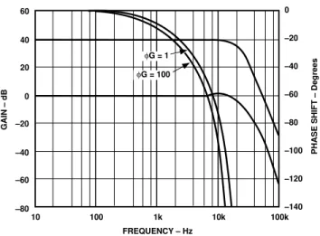
Phase Shift: Figure 10 illustrates the AD210’s low phase shift and gain versus frequency. The AD210’s phase shift and wide bandwidth performance make it well suited for applications like power monitors and controls systems.
60 20 –80 100 1k 10k 100k 10 40 –20 0 –60 –40 FREQUENCY – Hz 0 –20 –40 –60 –80 –100 –120 –140
PHASE SHIFT – Degrees
GAIN – dB
φG = 1
φG = 100
Figure 10. Phase Shift and Gain vs. Frequency
Input Noise vs. Frequency: Voltage noise referred to the input is dependent on gain and signal bandwidth. Figure 11 illustrates the typical input noise in nV/√Hz of the AD210 for a frequency range from 10 to 10 kHz. 60 40 0 100 1k 10k 10 50 20 30 10 FREQUENCY – Hz NOISE – nV/ √ Hz
Figure 11. Input Noise vs. Frequency
Gain Nonlinearity vs. Output: Gain nonlinearity is defined as the deviation of the output voltage from the best straight line, and is specified as % peak-to-peak of output span. The AD210B provides guaranteed maximum nonlinearity of ±0.012% with an output span of
±10 V. The AD210’s nonlinearity performance is shown in Figure 12. Gain Nonlinearity vs. Output Swing:The gain nonlinearity of the AD210 varies as a function of total signal swing. When the output swing is less than 20 volts, the gain nonlinearity as a fraction of signal swing improves. The shape of the nonlinearity remains constant. Figure 13 shows the gain nonlinearity of the AD210 as a function of total signal swing.
REV. A –6–
Isolated Power: The AD210 provides isolated power at the input and output ports. This power is useful for various signal conditioning tasks. Both ports are rated at a nominal ±15 V at 5 mA.
The load characteristics of the isolated power supplies are shown in Figure 15. For example, when measuring the load rejection of the input isolated supplies VISS, the load is placed
between +VISS and –VISS. The curves labeled VISS and VOSS are
the individual load rejection characteristics of the input and the output supplies, respectively.
There is also some effect on either isolated supplywhen loading the other supply. The curve labeled CROSSLOAD indicates the
sensitivity of either the input or output supplies as a function of the load on the opposite supply.
30 20 5 10 0 25 CURRENT – mA VOLTAGE VOSS VOSS VISS VISS SIMULTANEOUS SIMULTANEOUS CROSSLOAD 30
Figure 15. Isolated Power Supplies vs. Load
Lastly, the curves labeled VOSS simultaneous and VISS
simulta-neous indicate the load characteristics of the isolated power sup-plies when an equal load is placed on both supsup-plies.
The AD210 provides short circuit protection for its isolated power supplies. When either the input supplies or the output supplies are shorted to input common or output common, respectively, no damage will be incurred, even under continuous application of the short. However, the AD210 may be damaged if the input and output supplies are shorted simultaneously.
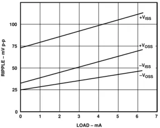
100 50 1 0 75 LOAD – mA RIPPLE – mV p-p –VOSS +VISS 30 25 0 +VOSS –VISS 2 3 4 5 6 7
Figure 16a. Isolated Supply Ripple vs. Load (External 4.7µF Bypass)
Under any circumstances, care should be taken to ensure that the power supplies do not accidentally become shorted.
The isolated power supplies exhibit some ripple which varies as a function of load. Figure 16a shows this relationship. The AD210 has internal bypass capacitance to reduce the ripple to a point where performance is not affected, even under full load. Since the internal circuitry is more sensitive to noise on the negative supplies, these supplies have been filtered more heavily. Should a specific application require more bypassing on the iso-lated power supplies, there is no problem with adding external capacitors. Figure 16b depicts supplyripple as a function of external bypass capacitance under full load.
1V 10mV 0.1µF 100mV 1mV CAPACITANCE
RIPPLE – Peak-Peak Volts
1µF 10µF 100µF
( )+VISS
+VOSS
( )–VISS
–VOSS
Figure 16b. Isolated Power Supply Ripple vs. Bypass Capacitance (Volts p-p, 1 MHz Bandwidth, 5 mA Load)
APPLICATIONS EXAMPLES
Noise Reduction in Data Acquisition Systems: Transformer coupled isolation amplifiers must have a carrier to pass both ac and dc signals through their signal transformers. Therefore, some carrier ripple is inevitably passed through to the isolator output. As the bandwidth of the isolator is increased more of the carrier signal will be present at the output. In most cases, the ripple at the AD210’s output will be insignificant when com-pared to the measured signal. However, in some applications, particularly when a fast analog-to-digital converter is used fol-lowing the isolator, it may be desirable to add filtering; other-wise ripple may cause inaccurate measurements. Figure 17 shows a circuit that will limit the isolator’s bandwidth, thereby reducing the carrier ripple.
VOUT 15 30 29 +VOSS +VISS –VISS +15V 2 4 –VOSS 14 1 0.001µF 0.002µF R (kΩ) = ( )f112.5 C (kHz) AD542 +VOSS –VOSS 3 VSIG 19 18 AD210 R R 16 17
Figure 17. 2-Pole, Output Filter
Self-Powered Current Source
The output circuit shown in Figure 18 can be used to create a self-powered output current source using the AD210. The 2 kΩ resistor converts the voltage output of the AD210 to an
equiva-REV. A –7– lent current VOUT/2 kΩ. This resistor directly affects the output
gain temperature coefficient, and must be of suitable stability for the application. The external low power op amp, powered by +VOSS and –VOSS, maintains its summing junction at output
common. All the current flowing through the 2 kΩ resistor flows through the output Darlington pass devices. A Darlington con-figuration is used to minimize loss of output current to the base.
IOUT 15 +VOSS +VISS –VISS +15V 2 –VOSS 14 1 LF441 +VOSS –VOSS 3 VSIG 0-10V 19 18 AD210 2kΩ 2N3906 (2) 16 17 4 FDH333 IOUT RETURN 30 29
Figure 18. Self-Powered Isolated Current Source
The low leakage diode is used to protect the base-emitter junc-tion against reverse bias voltages. Using –VOSS as a current
return allows more than 10 V of compliance. Offset and gain control may be done at the input of the AD210 or by varying the 2 kΩ resistor and summing a small correction current directly into the summing node. A nominal range of 1 mA– 5 mA is recommended since the current output cannot reach zero due to reverse bias and leakage currents. If the AD210 is powered from the input potential, this circuit provides a fully isolated, wide bandwidth current output. This configuration is limited to 5 mA output current.
Isolated V-to-I Converter
Illustrated in Figure 19, the AD210 is used to convert a 0 V to +10 V input signal to an isolated 4–20 mA output current. The AD210 isolates the 0 V to +10 V input signal and provides a proportional voltage at the isolator’s output. The output circuit converts the input voltage to a 4–20 mA output current, which in turn is applied to the loop load RLOAD.
RLOAD 15 +VOSS +VISS –VISS +15V 2 –VOSS 14 1 +VS –VS 3 VSIG 19 18 AD210 500Ω 2N2907 16 17 4 CURRENT LOOP 143Ω 3.0k ADJUST TO 4mA WITH 0V IN +28V CURRENT LOOP 2N2219 576Ω 1N4149 SPAN ADJ 100Ω 30 29 AD308
Figure 19. Isolated Voltage-to-Current Loop Converter
Isolated Thermocouple Amplifier
The AD210 application shown in Figure 20 provides amplifica-tion, isolation and cold-junction compensation for a standard J type thermocouple. The AD590 temperature sensor accurately
monitors the input terminal (cold-junction). Ambient tempera-ture changes from 0°C to +40°C sensed by the AD590, are can-celled out at the cold junction. Total circuit gain equals 183; 100 and 1.83, from A1 and the AD210 respectively. Calibration is performed by replacing the thermocouple junction with plain thermocouple wire and a millivolt source set at 0.0000 V (0°C) and adjusting RO for EOUT equal to 0.000 V. Set the millivolt
source to +0.02185 V (400°C) and adjust RG for VOUT equal to
+4.000 V. This application circuit will produce a nonlinearized output of about +10 mV/°C for a 0°C to +400°C range.
+VOSS +VISS –VISS +15V 2 –VOSS 3 18 AD210 16 17 4 13.7k 30 29 10k RG 5k A1 19 –VISS 10k 220pF 100k THERMAL CONTACT 52.3Ω COLD JUNCTION –VISS +VISS 1k -20k-"J" 15 14 1000pF 1 VOUT AD590 AD OP-07 RG
Figure 20. Isolated Thermocouple Amplifier
Precision Floating Programmable Reference
The AD210, when combined with a digital-to-analog converter, can be used to create a fully floating voltage output. Figure 21 shows one possible implementation.
The digital inputs of the AD7541 are TTL or CMOS compat-ible. Both the AD7541 and AD581 voltage reference are pow-ered by the isolated power supply + VISS. ICOMshould be tied to
input digital common to provide a digital ground reference for the inputs.
The AD7541 is a current output DAC and, as such, requires an external output amplifier. The uncommitted input amplifier internal to the AD210 may be used for this purpose. For best results, its input offset voltage must be trimmed as shown. The output voltage of the AD210 will go from 0 V to –10 V for digital inputs of 0 and full scale, respectively. However, since the output port is truly isolated, VOUT and OCOM may be freely
interchanged to get 0 V to +10 V.
This circuit provides a precision 0 V–10 V programmable refer-ence with a ±3500 V common-mode range.
+VOSS +VISS –VISS +15V –VOSS AD210 200Ω 1kΩ +VISS VOUT 0 - –10V 100kΩ 50kΩ 17 1 3 2 18 16 12-BIT DIGITAL INPUT AD7541 2kΩ GAIN HP5082-2811 OR EQUIVALENT +VISS AD581 OFFSET 17 15 4 1 3 2 18 16 4 15 19 14 30 29