HAL Id: hal-02869216
https://hal.archives-ouvertes.fr/hal-02869216
Submitted on 15 Jun 2020
HAL is a multi-disciplinary open access
archive for the deposit and dissemination of
sci-entific research documents, whether they are
pub-lished or not. The documents may come from
teaching and research institutions in France or
abroad, or from public or private research centers.
L’archive ouverte pluridisciplinaire HAL, est
destinée au dépôt et à la diffusion de documents
scientifiques de niveau recherche, publiés ou non,
émanant des établissements d’enseignement et de
recherche français ou étrangers, des laboratoires
publics ou privés.
Compact Modeling of 3D Vertical Junctionless
Gate-all-around Silicon Nanowire Transistors
Mukherjee Chhandak, Guilhem Larrieu, Cristell Maneux
To cite this version:
Mukherjee Chhandak, Guilhem Larrieu, Cristell Maneux. Compact Modeling of 3D Vertical
Junc-tionless Gate-all-around Silicon Nanowire Transistors. EuroSOI-ULIS 2020, Sep 2020, Caen, France.
�hal-02869216�
Compact Modeling of 3D Vertical Junctionless
Gate-all-around Silicon Nanowire Transistors
Chhandak Mukherjee
1, Guilhem Larrieu
2and Cristell Maneux
11IMS Laboratory, University of Bordeaux, France 2LAAS-CNRS, Université de Toulouse, France
AbstractThis paper presents a physics based,
computationally efficient compact modeling approach for 3D vertical gate-all-around junctionless nanowire transistor (JLNT) arrays designed for future high performance computational logic circuit. The model features an explicit continuous analytical form adapted for a 14 nm channel JLNT technology and has been validated against extensive characterization results on a wide range of JLNT geometry, depicting good accuracy. Finally, preliminary logic circuit simulations have been performed for benchmarking performances of transistor logic circuits, such as inverters and ring oscillators, designed using the developed model.
Keywords-Junctionless nanowire tranistors, compact model, high-speed logic circuit, heterogeneous integration.
I. INTRODUCTION
Data size and functionality requirements for computing systems are increasing rapidly with the expectation that hardware performance will continue to improve. For integrated circuit applications involving high-speed logic computing and low power dissipation, semiconductor technology scaling is mandatory. However, due to the anticipated end of conventional technological roadmap at the 7 nm gate node, it is becoming increasingly challenging for process engineers to maintain device functionality. Particularly, process challenges such as obtaining an abrupt shallow doping gradient at the source/drain junction, could be circumvented by junctionless nanowire transistors (JLNT) [1], due to high and uniform dopant concentration across its body and S/D regions. Combined with the merits of junctionless transistors such as high on/off current ratio or better electrostatic control in a gate-all-around (GAA) structure, vertical integration is an attractive approach because of its intrinsic 3D nature, which is more favorable for gate length and contact area scaling [2]. While JLNTs are certainly crucial building blocks for ultimate scaling of MOS transistors especially to support complex circuit architectures in high-speed logic applications, it is essential for the designers to have a physics-based, accurate, computationally efficient compact model which is independent of fitting parameters, has an explicit and continuous solution over the entire range of operation and is compatible with existing SPICE design framework. There have been several such modeling
approaches, including that of [3, 4], which have mainly focused on long-channel JLNTs. Moreover, most of these works have used TCAD data for model validation, and thus lack validation against experimental data from actual JLNTs. This work presents a compact modeling approach developed based on the physics-based JLNT compact model in [3] adapted for nanowire arrays of short channel JLNTs with gate lengths of 14 nm. The drain current equation has been modified to incorporate leakage and band-to-band tunneling currents and access region resistances. Moreover, the model accuracy has been validated against extensive measurements on an emerging vertical JLNT technology from LAAS [5, 6] that has also been exploited previously for extensive noise characterization [7, 8].
II. COMPACT MODEL FORMULATION
The model formulation is based on the unified charge-based control model (UCCM) elaborated in [3] for long-channel devices, which furthers the physical basis of the JLNT model presented in [4]. To overcome the limitations of the latter model, specifically in terms of the piece-wise continuous drain current model that requires additional smoothing functions and fitting parameters to bridge the depletion and accumulation modes of operation, the explicit and non-piece-wise solution in [3] treats the mobile charge (Qm) as decoupled between the
depletion (QDP) and complementary (QC) components. In
the depletion mode the UCCM expression has been formulated as [3], exp g th dep sc DP eff eff T sc V V V Q Q Q Q LW Q Q η ηφ − − = + (1) With the depletion charge, Qdep=qNDR/2, the effective
charge during depleteion, Qeff = QscηCoxφT/(Qsc+ηCoxφT),
Qsc=2εSiφT/R, R being the nanowire diameter, η being an
interface trap parameter, φT being the thermal voltage and
V is the potential along the channel. Lambert W
functions, LW, have been used in both [3] and [4] for developing the solution for total mobile charge in the JLNT. While the expression for QDP in (1) predicts the
depletion contribution correctly (for Vg<Vth), it
underestimates the value of the drain current above the flat-band condition. So in accumulation mode, especially in high accumulation, with QC≥Qdep, the charge QC has
that the threshold voltage is pinned at VFB in the
accumulation region, in order to avoid using additional smoothing functions and improve simulation time. Under high accumulation QC≥Qdep and QC is simplified using
another Lambert function as following [3],
exp g FB sc C c T c T T V V V Q Q C LW C η η φ η φ −ηφ − = (2) With corrected electrostatic control through Cc=Cox
-Ceff, Ceff=1/Cox+R/2εSi.
Having evaluated both the depletion and complementary parts of the mobile charge, one can formulate the non-pice-wise continuous model of the total drain current in terms of the QDP and QDC at the
source and the drain end, QDP0, QC0 and QDPL, QCL,
respectively,
(3) Here, η is an interface trap parameter with corrected electrostatic control in accumulation through Cc=Cox-Ceff,
Ceff=1/Cox+R/2εSi. The expression of drain current is free
of any fitting parameters and can be evaluated based on the physical device parameters such as that of geometry and doping. Additionally, short channel effects were also taken into account considering velocity saturation, an effective mobility, µeff, and incorporating an effective
gate length, Leff=L-ΔL, where L is the physical device
gate length and ΔL is calculated following [9],
(4)
With, vsat being the saturation velocity and S being a
parameter ensuring that ΔL tends to zero below the threshold, defined as [9],
(5) Where QDP0+QC0 is the total mobile charge at the source,
given by the long channel expression and B is a smoothing parameter. Furthermore, the short channel corrections incorporates an effective drain voltage, Vdeff,
through (4) that reaches its maximum at VSAT, the
saturation voltage [9],
(6) Here, A2 is another smoothing parameter for the transition of the drain voltage to VSAT. Considering that
the source and drain access region resistances degrade the drain current above threshold, the final expression of the drain current can be written as a function of the long channel current (IDS,0), using (3), taking into account the
corrections due to short-channel effects described by equations (4)-(6), as follows [9],
(7) Here, RS and RD are the source and drain series access
resistances, respectively; NF is the number of nanowires in parallel, η1 is a fine tuning parameter to take into
account the drain-voltage dependence of the series access resistances and QDP,Vdeff+QC,Vdeff is the total mobile charge
at the drain end (pinch-off) of the channel.
Additionally, considering formation of Schottky contacts at the source and drain access regions, the subthreshold leakage currents are also taken into account. Consequently, thermionic (Ith), tunneling (Itun) and
band-to-band tunneling (BTBT) contributions through gate-induced drain leakage (GIDL) are added as separate branch currents [10] to the total drain current, in order to model the subthreshold behavior of the drain current. The expression used in the compact model for the BTBT current at the drain end reads [10],
(8) With LAccess being the lengths of the source and drain
access regions outside the channel, BGIDL is a physics
based parameter with a theoretical value of 21.3 MV/cm [10] and Esegd is the electric field in the drain overlap
region, given as,
(9) Here, Vsegd is the gate-drain voltages across the oxide and
AGIDL, CGIDL are two GIDL fitting parameters.
Fig. 1: The vertical JLNT: (a) SEM image of nanowire arrays, (b) single nanowire showing its (c) gate formation (reproduced from [2]).
0 0 2 2 ,0 2 2 2 2 DP C DPL CL Q Q C DP DS eff T DP C Q eff ox T c T Q Q Q R I Q Q L C C π μ φ η φ η φ = + + +
(
)
2 0 0 0 2 2 1 1 ln 2 2 2 sat Si ox d deff d deff Si ox sat Si ox v R C V V V V R L S C v R C ε ε μ ε ε ε ε μ − + + − Δ = 0 0 1 1 1 DP C eff T S Q Q B C φ = − + + ln 1 exp 2 1 ln(1 exp( 2)) d SATdeff SAT SAT
V A V V V V A + − = − + ( 0 0,0) 1
(
0 0 ( , , ))
1 2 ( ) DS DSeff S D DP C DP C DP VDeff C VDeff eff I NF I R NF R R Q Q Q Q Q Q L π μ η = + + + − + − + 2 2 exp GIDL
GIDL Access GIDL DS segd
segd B I RL NF A V E E π = ⋅ −
(
)
2 2 0 ox segd GIDL DS segd Si C V C V E ε ε + =III. RESULTS AND DISCUSSIONS
The JLNT technology has a junction-less architecture composed of a homogenous highly doped nanowire channel (physical channel length of 14 nm), fabricated on boron doped (2×10¹⁹ /cm3) Si Substrate
, with the current
flowing between the silicided source/drain contacts being controlled by a gate-all-around structure (Fig. 1). More details on the fabrication steps can be found in [5].
A. Compact Model Validation
In this work, the compact model presented in the previous section is validated against measurement results on a wide range of geometries and test structures that have diameters (D) ranging between 22 and 50 nm with 16 to 625 nanowires in parallel (NF). Here we show results from nanowires with a diameter of 22 nm with different number of nanowires in parallel. Figs. 2 (a) and (b) show the ID-VGS and ID-VDS of a JLNT with 22 nm of
nanowire diameter and 16 nanowires in parallel. The model simulation results show very good agreement with the measurements over the entire bias range, indicating accuracy of individual modules of the compact model. A second order validation is performed in Figs. 2 (c) and (d) depicting the transconductance, gM, and output
conductance, gDS, of the JLNT, further affirming model
accuracy, despite a somewhat noisy measurements.
0.0 0.2 0.4 0.6 0.8 1.0 1.2 1.4 0.00 0.02 0.04 0.06 0.08 0.10 0.12 0.14 gDS ( m S ) -VDS( V) Measurement Compact Model D=22n NF=16 VGS= 0 to -2.0 in -0.25 V steps -0.4 -0.2 0.00.20.40.60.81.01.21.41.61.82.0 0.00 0.02 0.04 0.06 0.08 0.10 gM ( m S ) -VGS( V) Measurement Compact Model D=22n NF=16 VDS=-0.1 to -1.1 in -0.2 V step 0.0 0.2 0.4 0.6 0.8 1.0 1.2 1.4 0.00 0.02 0.04 0.06 0.08 0.10 D=22nm NF=16 VGS= 0 to -2.0 in -0.25 V steps -ID ( m A ) -VDS( V) Measurement Compact Model (a) (b) (c) (d) -0.4 -0.2 0.00.20.40.60.81.01.21.41.61.82.0 0.00 0.02 0.04 0.06 0.08 0.10 10-14 10-13 10-12 10-11 10-10 10-9 10-8 10-7 10-6 10-5 10-4 10-3 -ID ( m A ) -VGS( V) Measurement Compact Model -ID ( A ) D=22nm NF=16 VDS=-0.1 to -1.1 in -0.2 V step
Fig. 2: (a) ID-VGS, (b) ID-VDS (c) transcondunctance and (d) output
conductance of a JLNT with 22 nm diameter and 16 nanowires in parallel. (a) (b) -0.4 -0.2 0.00.20.4 0.60.81.01.21.41.61.82.0 0 1 2 3 4 5 10-12 10-11 10-10 10-9 10-8 10-7 10-6 10-5 10-4 10-3 -ID ( m A) -VGS( V) Measurement Compact Model D=22nm NF=625 -ID ( A) VDS=-0.1 to -1.6 in -0.25 V step 0.0 0.2 0.4 0.6 0.8 1.0 1.2 1.4 0 1 2 3 4 5 -ID ( m A) -VDS( V) Measurement Compact Model D=22nm NF=625 VGS= 0 to -2.0 in -0.25 V steps
Fig. 3: (a) ID-VGS, (b) ID-VDS of a JLNT with test structures having a
diameter 22 nm and 625 nanowires in parallel.
Extended model validation has been performed on two other test structures, with different geometries available from the same technology. Figs. 3 (a) and (b) show the ID-VGS and ID-VDS of JLNT test structures with a
diameter of 22 nm with 625 nanowires in parallel. Good model agreement is obtained in this case as well. Similar validation is depicted in Fig. 4 for a JLNT test structure with a diameter of 22nm and 400 nanowires in parallel, again depicting good agreement with the model simulation. (a) (b) 0.0 0.2 0.4 0.6 0.8 1.0 1.2 1.4 1.6 1.8 2.0 0.0 0.2 0.4 0.6 0.8 1.0 1.2 1.4 1.6 1.8 2.0 10-12 10-11 10-10 10-9 10-8 10-7 10-6 10-5 10-4 10-3 -ID ( m A) -VGS( V) Measurement Compact Model -ID ( A) D=22nm NF=400 VDS=-0.1 to -1.1 in -0.2 V step 0.0 0.2 0.4 0.6 0.8 1.0 1.2 1.4 1.6 1.8 2.0 0.0 0.1 0.2 0.3 0.4 0.5 0.6 0.7 0.8 0.9 1.0 1.1 1.2 -ID ( m A) -VDS( V) Measurement Compact Model D=22nm NF=400 VGS= 0 to -1.5 in -0.25 V steps
Fig. 4: (a) ID-VGS, (b) ID-VDS of a JLNT with test structures having a
diameter 22 nm and 400 nanowires in parallel.
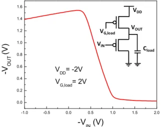
Slight discrepancies observed in the subthreshold region of operation will require further investigation and might require additional effects, such as drain-induced barrier lowering (DIBL), to be included within the model implementation and thus lies within the future scope of this work. -1.0 -0.5 0.0 0.5 1.0 1.5 2.0 0.0 0.2 0.4 0.6 0.8 1.0 1.2 1.4 1.6 VG,load= 2V
-V
OU T(V
)
-V
IN(V)
VDD= -2V VDD VOUT VG,load VIN CloadFig. 5: Transfer Characteristics of an inverter designed with two p-type JLNTs; inset: Schematic of the inverter circuit.
B. Circuit Demonstraion
Having validated the accuracy of the compact model at transistor level, we have exploited the model further for logic circuit demonstrations. As a first step toward benchmarking circuit simulation using the model, we have studied a simple inverter circuit designed using two p-type JLNTs (with NW diameters of 32 nm and 16 nanowires in parallel), as illustrated by the schematic shown in the inset of Fig. 5. The upper p-FET acts as an active load when applied a positive load bias, VG,load of
p-FET below. A supply voltage, VDD, of -2 V and a load
capacitance, Cload, of 1 fF have been used in the
simulation. Fig. 5 shows the transfer characteristics of the inverter which demonstrates a slight asymmetric yet a rather sharp switching from the high to the low state. Note that our previous works [5, 6] report a proof-of-concept CMOS inverter consisting of both n- and p-type JLNTs, which showed similar characteristics as the present work. -1.0 -0.5 0.0 0.5 1.0 1.5 2.0 0.0 0.5 1.0 1.5 VGload= 2V VDD= -2V
-V
OU T(V)
-V
IN(V)
VOUT9 VOUT1 VOUT2 VOUT3 VOUT4 VOUT5 VOUT6 VOUT7Fig. 6: Transfer Characteristics of a 9-stage ring oscillator depicting intermediate outputs of the cascaded stages.
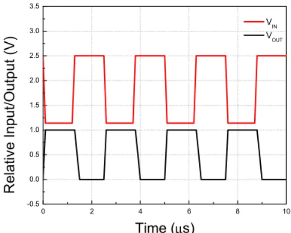
0 2 4 6 8 10 -0.5 0.0 0.5 1.0 1.5 2.0 2.5 3.0 3.5 R elat iv e In put /O utp ut (V) Time (μs) VIN VOUT
Fig. 7: Transient simulation of the inverter circuit depicting the input and the output waveforms.
Next, we have studied a 9-stage ring oscillator consisting of 9 inverter stages in cascade. Each inverter of the ring-oscillator has the same characteristics as shown in Fig. 5. In Fig. 6, the outputs of the different stages of the ring oscillator are shown on the voltage transfer characteristics (VTC). As observed from the figure, the output of the first stage resembles the VTC of the single stage inverter (Fig. 5), while the high-to-low transition continues to be sharper from one stage to the next. Although, the output of the 9th stage shows almost no
switching dissipation, from the output of the third stage onwards the transitions are quite similar and sharp. This
indicates that the optimum number of stages required is 3. Finally, Fig. 7 shows the transient simulation of the inverter circuit designed using two p-type JLNTs, demonstrating that for a given input signal VIN, the
output signal follows it in opposite phase, in accordance with classical inverter operation.
IV. CONCLUSIONS
In this work, we report a SPICE-compatible Verilog-A compact model for 14 nm gate-all-around vertical junctionless nanowire transistors, validated against extensive measurements on an emerging vertical JLNT technology. Good model accuracy has been observed over different geometries under study. The compact model has been exploited further for studying the performances of transistor logic circuits with active loads, including an inverter and a 9-stage ring oscillator. The proposed modeling framework will be indispensable for future high-performance logic circuit design.
ACKNOWLEDGEMENT
This work is supported by ANR under Grant ANR-18-CE24-0005-01
REFERENCES
[1] J.P. Colinge, C. W. Lee, A. Afzalian, et al., Nanowire transistors without junctions, Nat. Nanotechnol. vol. 5, pp. 225-229, 2010. [2] G. Larrieu and X.L. Han, Vertical nanowire array-based field effect transistors for ultimate scaling, Nanoscale, vol. 5, pp. 2437-2441, 2013.
[3] A. Hamzah, R. Ismail, N E. Alias, M. L. Peng Tan and A. Poorasl,Explicit continuous models of drain current, terminal charges and intrinsic capacitance for a long-channel junctionless nanowire transistor, Phys. Scr. vol. 94, pp. 105813, 2019. [4] F. Lime, O. Moldovan and B. Iñiguez, "A Compact Explicit
Model for Long-Channel Gate-All-Around Junctionless MOSFETs. Part I: DC Characteristics," IEEE Trans. Electron
Dev., vol. 61, no. 9, pp. 3036-3041, Sept. 2014. doi:
10.1109/TED.2014.2340441.
[5] Y. Guerfi and G. Larrieu,Vertical Silicon Nanowire Field EffectT ransistors with Nanoscale Gate-All-Around, Nanoscale research
letters, vol. 11, pp. 210, 2016.
[6] G. Larrieu, Y. Guerfi, X. L. Han and N. Clément Sub-15 nm gate-all-around field effect transistors on vertical silicon nanowires, Solid-State Electronics, vol. 130, pp. 9-14, 2017. [7] N. Clément, X. L. Han and G. Larrieu, Electronic transport
mechanisms in scaled gate-all-around silicon nanowire transistor arrays, Appl. Phys. Lett., vol. 103, pp. 263504-1-5, 2013. [8] C. Mukherjee, J. Pezard, G. Larrieu and C. Maneux, "1/f Noise in
3D vertical gate-all-around junction-less silicon nanowire transistors," Proc. 47th European Solid-State Device Research
Conference (ESSDERC), Leuven, 2017, pp. 34-37.
[9] F. Lim, F. Ávila-Herrera, A. Cerdeira and B. Iñiguez,A compact explicit DC model for short channel Gate-All-Around junctionless MOSFETs, Solid State Electron, vol. 131, pp. 24-29, 2017. [10] G. Zhu et al., "Subcircuit Compact Model for Dopant-Segregated
Schottky Gate-All-Around Si-Nanowire MOSFETs," Trans.
Electron Dev., vol. 57, no. 4, pp. 772-781, April 2010. doi:
![Fig. 1: The vertical JLNT: (a) SEM image of nanowire arrays, (b) single nanowire showing its (c) gate formation (reproduced from [2])](https://thumb-eu.123doks.com/thumbv2/123doknet/14262667.489485/3.892.110.369.596.740/vertical-nanowire-arrays-single-nanowire-showing-formation-reproduced.webp)