HAL Id: hal-01760571
https://hal.archives-ouvertes.fr/hal-01760571
Submitted on 29 Jul 2020
HAL is a multi-disciplinary open access
archive for the deposit and dissemination of
sci-entific research documents, whether they are
pub-lished or not. The documents may come from
teaching and research institutions in France or
abroad, or from public or private research centers.
L’archive ouverte pluridisciplinaire HAL, est
destinée au dépôt et à la diffusion de documents
scientifiques de niveau recherche, publiés ou non,
émanant des établissements d’enseignement et de
recherche français ou étrangers, des laboratoires
publics ou privés.
Dynamic behavior of silicon nanocrystal memories
during the hot carrier injection
V. Della Marca, L. Masoero, J. Postel-Pellerin, F. Lalande, J. Amouroux, J.
Delalleau, P. Boivin, J-L. Ogier, G. Molas
To cite this version:
V. Della Marca, L. Masoero, J. Postel-Pellerin, F. Lalande, J. Amouroux, et al.. Dynamic behavior of
silicon nanocrystal memories during the hot carrier injection. IEEE International Conference on Solid
Dielectrics (ICSD 2013), Jun 2013, Bologne, Italy. �10.1109/ICSD.2013.6619820�. �hal-01760571�
Dynamic Behavior of Silicon Nanocrystal Memories
During the Hot Carrier Injection
V. Della Marca, L. Masoero, J. Postel-Pellerin,
F. Lalande
Im2np-CNRS, Université Aix-Marseille, Marseille, France [email protected]
J. Amouroux, J. Delalleau, P. Boivin, J-L. Ogier
STMicroelectronics, 13106 Rousset, France
G. Molas
CEA-LETI, MINATEC, Grenoble, France
Abstract—In this paper we present the last improvement on programming window and consumption of silicon nanocrystal memory cell (Si-nc). Using a dynamic technique to measure the drain current during the hot carrier injection (HCI) programming operation, we explain the behavior of Flash floating gate (F.G.) and silicon nanocrystal memories. We use TCAD simulations to reproduce the charge diffusion in the nanocrystal trapping layer in order to understand the physical mechanism. Finally experimental results of electrical characterizations are shown using different bias conditions to compare the devices.
Keywords—Silicon nanocrystal memory, charge diffusion, energy consumption.
I. INTRODUCTION
Silicon nanocrystal memory (Si-nc) is one of the most promising devices to replace the Flash floating gate (F.G.) for NOR embedded applications. The robustness against leakage currents (SILC) and the reduced process mask number are two of the main features of this device [1, 2]. High-k materials were integrated in 1T cell in order to improve the programming window and reliability [3, 4]. Moreover split gate (1.5T) architectures were proposed to reduce the current consumption [5, 6]. In a previous work on Si-nc cell we have shown the sub-nanojoule energy consumption during a hot carrier injection (HCI) programming operation [7]. In this paper we deeply analyze the dynamic silicon nanocrystal cell behavior in order to explain the improvement on drain current consumption achieved when the cell covered area is increased and the silicon nitride (SiN) capping layer on Si-nc is removed. With the means of 2D TCAD simulations we understand the dynamic Si-nc cell behavior and we compare it with a standard Flash floating gate memory cell. The charge diffusion mechanism between neighbor nanocrystals is highlighted enabling a double transistor cell functioning. Finally the electrical characterizations are thus used to find the best trade-off between the programming scheme and the cell architecture.
II. TECHNICAL DETAILS
A. Silicon Nanocrystals Deposition
In this study the silicon nanocrystals were grown on thin silicon oxide (SiO2) by two steps Low Pressure Chemical Vapor Deposition (LPCVD) recipe. The top surface of tunnel oxide was chemically prepared to increase the number of nucleation sites; this cleaning step impacts the final tunnel oxide thickness [8]. The nanocrystal two steps process was used in either epitaxy tool or in industrial LPCVD furnace. The nucleation step was obtained by silane (SiH4) diffusion on hydroxyl tunnel oxide surface. The second step consists in a selective growth achieved by using dichlorosilane (SiH2Cl2) diffusion. Thanks to these two steps, the silicon nanocrystal size and density can be controlled independently. The nucleation controls the number of Si-nc on top surface of tunnel oxide while the size is monitored by the selective growth period [9].
B. Samples description
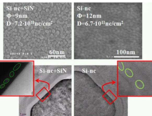
The samples used in this work are silicon nanocrystal and floating gate memory cells integrated on 200mm wafers. The size and density of silicon nanocrystals were controlled in-line using an image processing technique of a critical dimension scanning electron microscopy (CDSEM) picture [10]. Two types of samples with and without SiN capping layer on Si-ncs, are compared with a floating gate cell, the samples description is reported in Table I. At the end of process TEM analyses were used to check the silicon nanocrystals integrity in the memory stack. In Fig. 1 we show the CDSEM pictures used to measure the Si-nc size and density, and the TEM images of the silicon nanocrystal samples described in Table I.
TABLE I. SAMPLES DESCRIPTION (TUNOX:TUNNEL OXIDE THICKNESS, Φ:NANOCRYSTALS AVERAGE DIAMETER;D:NANOCRYSTALS DENSITY,C:
COVERED AREA;ONO:EOT OF INTERPOLY DIELECTRIC LAYER).
tunox
(nm) (nm) Φ (nc/cmD 2) ONO (nm) C (%)
F.G. 9.5 14.5 100 Si-nc 4.2 12 6.7·1011 10.5 76
Fig. 1. Critical Dimension Scanning Electron Microscopy (top) pictures and Transmission Electron Microscopy (bottom) images of silicon nanocrystal cells with and without SiN capping layer.
III. PHYSICAL UNDERSTANDING
We demonstrated in recent studies how it is possible to improve the silicon nanocrystal memory performance increasing the cell coupling factor by using a thinner memory stack and increasing the nanocrystal size, thus the covered area [11]. With the dynamic method described in [12] we measured the current consumed during HCI programming for the three devices described in Table I. The normalized drain currents reported in Fig. 2 are measured applying a gate voltage (Vg) of 9V and a drain voltage (Vd) of 4.2V. The programming time (tp) was fixed to 5µs. We explained in [11] the transistor-like behavior of hybrid Si-nc+SiN cell where the drain current follows the gate potential, remaining constant during the programming, due to the localization of trapped charge. On the contrary, for the floating gate device, a current peak is detected when the HCI starts, while during the pulse the current exponentially decreases. In Fig. 2 we show the behavior of a Si-nc cell where large nanocrystals (Φ=12nm) with a high density are embedded. In this case an intermediate response is noticed. During the hot carrier injection the charges flow throw the silicon nanocrystals toward the source side modifying the substrate surface potential, thus the electric field.
Fig. 2. Dynamic drain currents measured for silicon nanocrystal (Si-nc), floating gate (F.G.) and silicon nanocrystals with nitride capping (Si-nc+SiN) cells, during hot carrier injection.
A. Simulation of charge diffusion
The charge diffusion mechanism in silicon nanocrystal layer was emulated using a commercial TCAD simulator. We chose a two-dimensional approach in order to: evaluate the process impact, improve the program stability and reduce the simulation time. The process was simulated using the parameters set provided by Advanced Calibration, and the electrical simulations with Sentaurus Device 2010.3.The charge diffusion can be due to the single electron interactions between neighbor silicon nanocrystals with different electric potentials [13]. Moreover the nanocrystal coalescence during the growth process can reduce the distances up to the contact creating percolative paths from the drain side to the source side in the charge trapping layer. The simulation of dynamic charge tunneling between neighbor nanocrystals during the HCI requires a too high computational cost and convergence is hard to reach. For the simulations (Fig. 3a) we thus considered four different samples (s0, s1, s2, s3), where the quantity of stored charge after the dynamic HCI is shown in Fig. 3b. Hereafter we emulated the charge diffusion in nanocrystal trapping layer allocating arbitrary charge close to the source region (Fig. 3c). The charge diffusion was compensated by the programming, and the quantity of charge on the drain side is kept constant. The simulated drain current during the programming operation for the considered samples is reported in Fig. 4a and compared with the experimental data (Fig. 4b). One can notice that increasing the quantity of trapped charge in Si-ncs close to the source region, the drain current absorption decreases. Hence the charge diffusion toward the source side can explain the lowering of consumed current during a HCI operation as shown in Fig. 4a.
Fig. 3. (a) Structure of the simulated silicon nanocrystal cell. (b) Position of trapped charge in silicon nanocrystal cell after dynamic HCI. (c) Simulated charge position considering the charge diffusion.
Fig. 4. (a) Simulated drain current during hot carrier injection considering the samples of Fig. 3; (b) and comparison with the experimental data.
B. Double Transistor Behavior
In association with the current consumption we simulated also the programming window after the hot carrier injection considering the samples of Fig. 3. The programming window depends on the position of the potential minimum [14], thus on the position of the nanocrystal with the highest amount of trapped charge. In Fig. 5 we show that the simulated charge trapping in the source side weakly impacts the programming window (variation of 8%). We can conclude that the charges in silicon nanocrystals positioned on the drain side (HCI zone) can control the programming window, while the stored charges in Si-ncs close to the source, control the consumed current. The charge diffusion changes the cell behavior emulating a double transistor functioning (Fig. 6) where the transistor on the source side acts as an access transistor with a threshold voltage that depends on the quantity of the trapped charges. To increase the ability to control the channel current, one way is to increase the charge diffusion toward the source side. As shown in Fig. 2, this result can be reached decreasing the distances between the nanocrystals up to the contact and thus creating percolative paths from the drain to the source side.
IV. ELECTRICAL CHARACTERIZATION
Taking into account the dynamic behavior of Si-nc cell and the fact that, for short pulse durations, the box is more efficient with respect the ramp pulse [7], we performed the consumption measurements varying the drain and gate biases and we compared the results with the hybrid Si-nc+SiN cell.
A. Si-nc cell performance
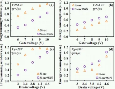
In Fig. 7 we reported the programming window and the energy consumption as a function of Vg (a-b) and Vd (c-d) using 1µs programming pulses, of Si-nc and Si-nc+SiN cells.
Fig. 5. Simulated programming window for each sample of Fig. 3, the dependance on charge diffusion is highlighted.
Fig. 6. Schematic of silicon nanocrystal cell when the charge diffusion mechanism is enabled.
We notice that the silicon nanocrystal cell shows a better programming window due to the higher covered area, and lower energy consumption thanks to the charge diffusion. For the two samples the gate voltage dependence is linear. On the contrary with the high drain voltage the programming window tends to saturate when Vd corresponds to 3.8V for the Si-nc cell and for Vd greater than 4.6V for Si-nc+SiN sample, while the energy exponentially increases, because the hot carrier generation. These results impact the cell efficiency that is defined as the ratio between the programming window and the energy consumption. In Fig. 8a one can notice that for the Si-nc cell the efficieSi-ncy decreases as gate voltage decreases. This is because a lower Vg is sufficient to reach the programming window close to the saturation level, while the drain current dependence with Vg, increases the consumed energy. On the other hand, varying the drain voltage we note that the efficiency is strongly increased with respect to the Si-nc+SiN cell (Fig. 8b), the optimization point of Si-nc cell is reached at Vd=3.8V, thus when the programming window starts to saturate (Fig. 7c). The decreasing of optimized programming drain voltage down to 3.8V is important not only for the consumption gain, but also allows reducing the size of charge pump circuits, that can deliver less current to the memory array.
Fig. 7. Programming window and energy consumption versus gate voltage (a-b) and drain voltage (c-d); silicon nanocrystal (Si-nc) and hybrid silicon nanocrystal (Si-nc+SiN) cells are compared. The Y scales are normalized to the same value.
Fig. 8. Silicon nanocrystal nc) and hybrid silicon nanocrystal (Si-nc+SiN) cell efficiency are compared as a function of gate (a) and drain (b) voltage.
The area reduction of these circuits impacts directly the final chip cost, thus the importance of this improvement. Finally we plotted in Fig. 9 the consumed energy as a function of the programming window, comparing the two nanocrystal devices. The Si-nc cell shows 20% programming window gain keeping constant the consumed energy level. Dependently on final purpose it is possible to decrease the programming time in order to reduce the energy consumption for very fast and ultra low energy applications.
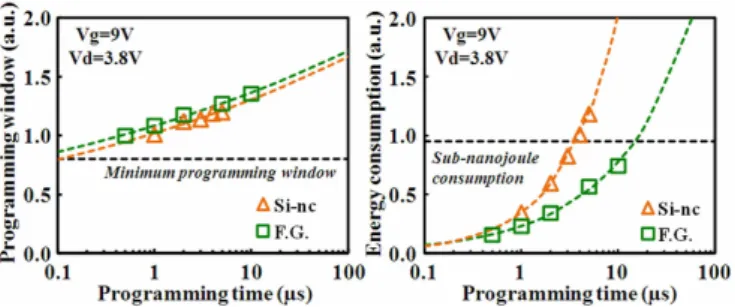
B. Flash Floating Gate Performance: Benchmark
We complete the study on Si-nc cell consumption comparing it with the results of F.G. device shown in [12]. We plot in Fig. 10 the programming window and the consumed energy of Si-nc and F.G. cells as a function of the programming time. The biasing condition used in this case is: Vg=9V and Vd=3.8V corresponding to the optimization for each memory device. The Si-nc cell is able to reach a programmed level comparable with the F.G. cell, but the consumed energy remains more important because of the higher drain current. Using the experimental data we extrapolated the power laws able to describe the cells behaviors and we show that using very fast pulses the Si-nc consumption can be improved achieving the F.G. performance. Furthermore the dynamic measurements allowed to verify the presence of drain current peak that can disturb the circuits around the memory array [15]. In case of Si-nc the advantage is that the current decreasing is not abrupt and it can be tolerated by the design constraints.
Fig. 9. Energy consumption as a function of programming window. The optimized Si-nc and hybrid Si-nc+SiN cells are compared. The application targets are highlighted.
Fig. 10. Programming window and energy consumption of silicon nanocrystal (Si-nc), and floating gate (F.G.) cells.
V. CONCLUSION
In this paper the dynamic behavior during the HCI operation, of Si-nc memories with and without SiN capping layer and of F.G. memory has been compared. The experimental results have been explained with the means of 2D TCAD simulations. We correlated the dynamic behavior of Si-nc cell with the charge diffusion in nanocrystal trapping layer. We explained the lowering of the consumed current with a double transistor cell behavior, where the charge redistribution in trapping layer leads to control the consumed current. Electrical characterizations have also been performed using various bias conditions. Because of the increased cell covered area and consequently charge diffusion, the Si-nc devices have a higher efficiency than the Si-nc+SiN memories. The maximum efficiency of Si-nc cell is reached for a Vd of 3.8V. We reported a gain of 20% on programming window with respect to Si-nc+SiN cell and sub-nanojoule consumption. Finally the optimized Si-nc cell is compared with the F.G. reaching almost the same performance for short programming pulse. The Si-nc cell is thus suitable for very fast and ultra low energy application, moreover decreasing both the disturb due to the drain current peak and the process mask number.
REFERENCES
[1] C. M. Compagnoni et al., Study of data retention for nanocrystal Flash memories", proc. of IRPS, pp. 506-512, 2003.
[2] B. De Salvo et al., How far will silicon nanocrystals push the scaling limits of NVMs technologies?, Tech. Dig. of IEDM, pp. 597-600, 2003. [3] G. Molas et al., Thorough investigation of Si-nanocrystal memories with
high-k interpoly dielectrics for sub-45nm node Flash NAND applications, proc. of IEDM, pp. 453-456, 2007.
[4] G. Gay et al., Performance and Modeling of Si-Nanocrystal Double-Layer Memory Devices With High- k Control Dielectrics, IEEE Trans. on Elec. Dev., vol. 59, pp. 933-940, 2012.
[5] L. Masoero et al., Physical Understanding of Program Injection and Consumption in Ultra-Scaled SiN Split-Gate Memories, proc. of IMW, pp. 1-4, 2012.
[6] J. Yater et al., Highly Optimized Nanocrystal-Based Split Gate Flash for High Performance and Low Power Microcontroller Applications, proc. of IMW, pp. 1-4, 2011.
[7] V. Della Marca et al., Optimization of programming consumption of silicon nanocrystal memories for low power applications, proc. of ISCDG, pp. 65-68, 2012.
[8] F. Mazen et al., Influence of the Chemical Properties of the Substrate on Silicon Quantum Dot Nucleation, J. Electrochem. Soc. vol. 150, pp. G203-G208, 2003.
[9] F. Mazen et al., Appl. Surf. Sci. vol. 214, pp. 359-363, 2003.
[10] J. Amouroux et al., Extraction of physical parameters on silicon nanocrystals devoted to non-volatile memories, proc. of ISCDG, pp. 169-172, 2012.
[11] V. Della Marca et al., How to improve the silicon nanocrystal memory cell performances for low power applications, proc of CAS, pp. 103-106, 2012.
[12] V. Della Marca et al., Push the flash floating gate memories toward the future low energy application, Solid-State Electronics, vol. 79, pp. 210-217, 2013.
[13] H. Matsuoka et al., Single electron charging effect in coupled quantum dots of a Si-MOSFET, proc. of IEDM Tech. Dig., pp. 781-784, 1992. [14] Z. H. Liu et al., Threshold voltage model for deep-submicrometer
MOSFETs, IEEE Trans on Elec. Dev., vol. 40, pp. 86-95, 1993.
[15] D. Munteanu et al., Modeling of drain current overshoot and recombination lifetime extraction in floating-body submicron SOI MOSFETs, IEEE Trans. on Elec. Dev., vol. 49, pp. 1198-1205, 2002.