HAL Id: hal-02292390
https://hal.sorbonne-universite.fr/hal-02292390
Submitted on 19 Sep 2019
HAL is a multi-disciplinary open access
archive for the deposit and dissemination of
sci-entific research documents, whether they are
pub-lished or not. The documents may come from
teaching and research institutions in France or
abroad, or from public or private research centers.
L’archive ouverte pluridisciplinaire HAL, est
destinée au dépôt et à la diffusion de documents
scientifiques de niveau recherche, publiés ou non,
émanant des établissements d’enseignement et de
recherche français ou étrangers, des laboratoires
publics ou privés.
Functional hybrid multilayered van der Waals
heterostructures from graphene and self- assembled
supramolecular 2D crystals
Nataliya Kalashnyk, Anaïs Gouesmel, Eunkyoung Kim, André-Jean Attias,
Fabrice Charra
To cite this version:
Nataliya Kalashnyk, Anaïs Gouesmel, Eunkyoung Kim, André-Jean Attias, Fabrice Charra.
Func-tional hybrid multilayered van der Waals heterostructures from graphene and self- assembled
supramolecular 2D crystals. 2D Materials, IOP Publishing, 2019, 6 (4), pp.045016.
�10.1088/2053-1583/ab2ba7�. �hal-02292390�
HAL Id: hal-02292390
https://hal.sorbonne-universite.fr/hal-02292390
Submitted on 19 Sep 2019
HAL is a multi-disciplinary open access
archive for the deposit and dissemination of
sci-entific research documents, whether they are
pub-lished or not. The documents may come from
teaching and research institutions in France or
abroad, or from public or private research centers.
L’archive ouverte pluridisciplinaire HAL, est
destinée au dépôt et à la diffusion de documents
scientifiques de niveau recherche, publiés ou non,
émanant des établissements d’enseignement et de
recherche français ou étrangers, des laboratoires
publics ou privés.
heterostructures from graphene and self- assembled
supramolecular 2D crystals
Nataliya Kalashnyk, Anaïs Gouesmel, Eunkyoung Kim, André-Jean Attias,
Fabrice Charra
To cite this version:
Nataliya Kalashnyk, Anaïs Gouesmel, Eunkyoung Kim, André-Jean Attias, Fabrice Charra.
Func-tional hybrid multilayered van der Waals heterostructures from graphene and self- assembled
supramolecular 2D crystals. 2D Materials, IOP Publishing, 2019, 6 (4), pp.045016.
�10.1088/2053-1583/ab2ba7�. �hal-02292390�
IOP Publishing
Journal Title
Journal XX (XXXX) XXXXXX
https://doi.org/XXXX/XXXX
xxxx-xxxx/xx/xxxxxx 1
Functional hybrid multilayered van der Waals
heterostructures from graphene and
self-assembled supramolecular 2D crystals
Nataliya Kalashnyk
1,3, Anaïs Gouesmel
1, Eunkyoung Kim
2,4, André-Jean Attias
3,4and Fabrice Charra
11 SPEC, CEA/CNRS, UMR 3680, Université Paris-Saclay, CEA Saclay, 91191 Gif-sur-Yvette Cedex,
France
2 Department of Chemical and Biomolecular Engineering, Yonsei University, 50 Yonsei-ro,
Seodaemun-gu, Seoul, Korea
3 Institut Parisien de Chimie Moléculaire, CNRS UMR 8232, Sorbonne Université, 4 Place Jussieu,
75252 Paris Cedex, France
4 Building Blocks for Future Electronics Laboratory, CNRS/Sorbonne Université/Yonsei University,
UMI 2002, Yonsei University, 50 Yonsei-ro, Seodaemun-gu, Seoul, Korea E-mail: [email protected] and [email protected]
Received xxxxxx
Accepted for publication xxxxxx Published xxxxxx
Abstract
We demonstrate the soft realization of a new generation of functional hybrid van der Waals (vdW) heterostructures alternating two-dimensional (2D) materials and surface-confined supramolecular self-assemblies of porous crystals into three-dimensional (3D) stacks. We show that graphene can be transferred on top of a graphite-confined self-assembled 2D porous network, the cavities of which might be filled with functional guests. Subsequent growth of a new 2D host-guest self-assembled monolayer on top of this intermediate vdW heterostructure further extends it into the third dimension. Thus, this versatile approach, potentially not limited in the number of layers, allows creating on demand sequences by the careful choice of the 2D materials and of the presence or not and choice of guest molecules and permits to envisage innovative structures such as record-density bulk heterojunctions.
Keywords: hybrid van der Waals heterostructures, multilayered materials, graphene, surface-confined supramolecular self-assembly, host-guest chemistry, scanning tunnelling microscopy
1. Introduction
Designing van der Waals (vdW) heterostructures based on two-dimensional (2D) materials is blossoming as a promising route in nanoscience to the fabrication of new-generation tailored systems and devices with unique functionalities [1-6]. Several types of vdW heterostructures are obtained depending on the components integrated into the stacked architectures.
Archetypal vdW heterostructures are created by combining, in vertically stacked structures, individual sheets of 2D crystals -such as graphene, hexagonal boron nitride (h-BN), molybdenum disulphide (MoS2), and other
transition-metal dichalcogenides (TMDs)- held together by van der Waals forces [1-3]. These all-2D vdW heterostructures exhibit improved properties compared to individual components and have been used to create innovative atomically thin devices [4].
VdW heterostructures can also be built by assembling through vdW interactions organic materials onto 2D layered materials used here as substrates, leading to organic/2D vdW heterostructures [5,6]. The integration of the organic layer into such hybrid heterostructures is achieved in different ways, ranging from epitaxial growth of molecular crystal to formation of a self-assembled monolayer [7-10]. The growth of the organic monolayer physisorbed onto a 2D atomic crystal by supramolecular self-assembly of molecular building blocks is of particular interest. It allows forming of a wide variety of 2D networks with different topologies on the one hand, and the non-covalent functionalization of the 2D substrate on the other hand [11-16]. In most cases, the guidelines developed for 2D supramolecular self-assembly on highly oriented pyrolytic graphite (HOPG) [17,18], are extended to the 2D substrate, mostly graphene. The molecular units are conjugated molecules equipped with peripheral alkyl chains that drive the supramolecular self-assembly on sp2-hybridized carbon-based substrates. The alkyl chains epitaxy with the lattice structure of the underlying carbon network as well as their interdigitation, both mainly governed by van der Waals interactions, favor the formation of well-ordered 2D molecular crystals. However, the hybrid vdW heterostructures are so far restricted to a simple sequence consisting in only one organic layer adsorbed on a layered 2D material.
In this context, one can think of expanding the family of vdW heterostructures towards multilayered functional vdW heterostructures by integrating and alternating 2D atomic crystals and 2D self-assembled organic crystals. Such a strategy becomes even more attractive and powerful if the stacking sequences integrate organic 2D porous networks. By possibly acting as host matrix for recognition and selective co-adsorption of functional guest molecules they allow 2D host-guest chemistry as well as a functionalization of the heterostructures.
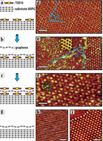
Here, we demonstrate that new functional multilayered vdW heterostructures can be created by an iterative procedure combing vdW heterostructure and 2D host-guest chemistry approaches. We report two prototype heterostrutures, P1 and P2 obtained as illustrated in Scheme 1 and detailed in the Experimental section. In brief, a monolayer of a 2D self-assembled supramolecular porous network is first grown on a HOPG substrate, a 3D stack of graphene sheets itself. Then, a CVD-grown copper monolayer graphene is transferred via a wet process onto the 2D porous host adlayer, possibly filled with functional guest molecules. Finally, to vertically expand this structure, the topmost graphene monolayer cover is further functionalized with a self-assembled porous network possibly trapping guest molecules. The sample surfaces are investigated at each stage of the stacking process by scanning tunnelling microscopy (STM) at room temperature and at air/solid interface.
i) ii) iii) iv) v)
i) ii) iii) iv) v)
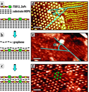
Scheme 1. Schematic representations of the manufacturing processes that leads to the targeted P1 and P2 hybrid vdW heterostructure prototypes. a. P1 hybrid vdW heterostructure prototype. i): drop-casting on HOPG of the TSB10 molecules from toluene solution. ii),iii): transfer of graphene supported by PMMA (green) carrier, after etching its copper substrate (see Supporting Information Scheme S1). iv): removal of PMMA carrier. v): drop-casting of the second layer of the TSB10 molecule from toluene solution. b. P2 hybrid vdW heterostructure prototype. i): drop-casting on HOPG of the (TSB12+ZnPc) guest-host stoichiometric mixture from toluene solution. ii),iii): transfer of graphene supported by PMMA carrier, after etching its copper substrate (Scheme S1). iv): removal of PMMA carrier. v): drop-casting of the second layer of the (TSB12+ZnPc) guest-host mixture from toluene solution. For molecular structures of TSB10, TSB12, and ZnPc, see Scheme 2.
We show that the surface-confined molecular network sandwiched between HOPG and graphene is unaltered during the wet transfer process. Moreover, we demonstrate that the neat graphene face remains suitable for supramolecular self-assembly despite the graphene monolayer is supported by a soft organic layer. It is remarkable, since the self-assembly of molecules on graphene is always achieved by using single layers supported by a solid substrate on which graphene was either grown or transferred. Overall, we provide a general strategy for the integration at will of various 2D materials and 2D functional organic crystals into multilayered hybrid vdW heterostructures.
2. Results
2.2 Choice of materials
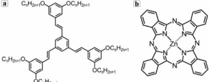
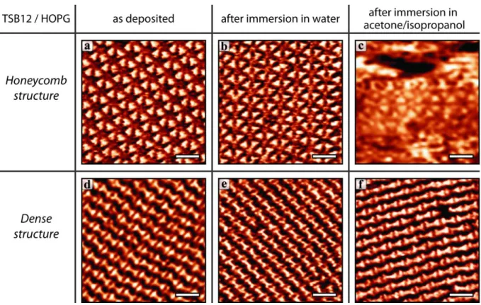
As molecular units, we chose alkoxy-substituted conjugated tristilbene cores (Scheme 2) [19], denoted hereafter TSB-Cn with n the number of methylene units in the alkoxy chains. These building blocks form strongly adsorbed self-assembled supramolecular structures on both HOPG [20] or graphene [2]. TSB-Cn can form either porous honeycomb networks or compact networks (Figure S1a,c,d). The dense compact phase is the thermodynamically stable one at liquid-solid interface for solute concentrations above a critical one, whereas the porous phase is stable below this concentration. The complete monolayers are kinetically blocked at room temperature, the thermodynamically stable structure being reached only through thermal ripening [22]. The porous phase is able to host third-party functional molecules while keeping its honeycomb structure (Figure S1b) [23-25]. Moreover, their lipophilic character make them likely to withstand wet transfer processes. The choice of HOPG as starting substrate rather than graphene was necessary for better image analysis by STM. Actually, the CVD-grown graphene on copper substrate imposes a roughness to the global image contrast which dominates over local molecular contrast in STM.
2.2
Building
steps
and
characterization
of
heterostructure prototype P1
For the proof of concept demonstration, we first build the P1 model prototype that integrates TSB10 as network molecular unit. For the first stage of the fabrication process (Figure 1a), we chose TSBC10 solution concentration close to the critical one, i.e. 10-4 mol.l-1, and room temperature
deposition without ripening stage. The aim was to intentionally form coexisting dense and porous domains (Figure 1d), as formed during the surface nucleation and growth process. The bright patterns in STM imaging are the result of increased electron tunnelling through conjugated molecular cores, whereas non-conjugated alkyl chains produce lesser contrast. As shown later, the coexistence of two
Scheme 2. Molecular structures of host and guest molecules. a. Molecular structure of the TSB-Cn molecule that forms the honeycomb 2D host matrix. b. Molecular structure of the Zinc Phthalocyanine (ZnPc) guest molecule.
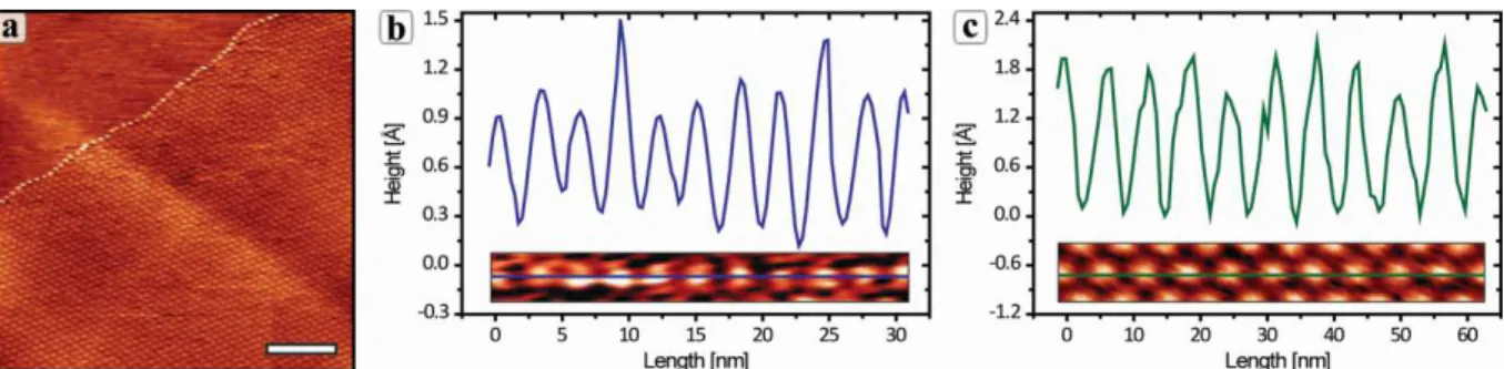
types of patterns will help to prove through STM image analysis the multilayered heterostructure formation after the graphene transfer stage. After confirming that the TSB-Cn adsorbed monolayer is intact for a series of assays including the wet-transfer procedure, solvent and thermal treatments (see Experimental section and Figure S2), we transferred on top of the previous hybrid heterostructure a graphene monolayer initially CVD-grown on copper foil (Figure 1b). Figure 1e shows a typical STM image after the top graphene layer deposition. We indirectly infer from this image that we observe an area with similar coexistence of both porous and dense domains as in Figure 1d. First, triangular lattices are observed on the sandwich structure with a period (3.75±0.2 nm) compatible, within experimental uncertainties, with that of the honeycomb lattice (3.82 nm) of the buried TSB10 monolayer (Figure S3a-c). Surprisingly, however, they present a single triangular (i.e. centered hexagonal) structure rather than the honeycomb structure of TSB10. This can be attributed to the formation of trapped aqueous clusters formed inside the pores of the honeycomb lattice during the wet transfer procedure and producing protrusions on the graphene layer with the observed periodicity [26]. Domains of lamellas are also observed. Their periodicity (2.7 ±0.2 nm) (Figure S3d-f), as well as the relative angle (α = 70±5°) with the neighboring triangular domain (Figure 1d,e) are compatible with domains of the dense lattice formed by TSB10. Following these interpretations, the comparison of Figure 1d and Figure 1e emphasizes the different origin of contrast for the imaging of the uncovered molecular lattice and the buried one. Whereas the STM response of the former results from increased tunnelling through conjugated part, the STM contrast of the latter corresponds to the imaging of the deformations mechanically induced on the top graphene layer and thus equally reflects conjugated and saturated molecular moieties.
To further confirm the interpretations of the above-described patterns, we prepared a control sample by transferring graphene on a freshly-cleaved bare HOPG substrate, without TSB molecules, following strictly the same procedure as above (see schematic drawing in Figure 1g). The obtained STM images of this control sample are strikingly
4 Figure 1. Three-component hybrid multilayer vdW heterostructure. (a-c) Schematics of the architectures at each stage of the fabrication process: (a) HOPG/TSB10, (b)
HOPG/TSB10/Graphene, and (c)
HOPG/TSB10/Graphene/TSB10 heterostructures. (d-f) STM images of co-existing dense and honeycomb molecular patterns of TSB10 molecules directly self-assembled on HOPG surface (d), graphene-covered (e), and subsequently covered by a TSB10 self-assembled layer (f). Superimposed: on (e) a zoom showing the graphite atomic honeycomb lattice (0.244 nm) ; on (f) a honeycomb motif formed from conjugated kernels of TSB10 units (green triangles) (g-i) Control sample: schematic (g) and STM images of the Moiré patterns with periodicity of 3 nm (h) and 6 nm (i) found upon transfer of graphene on HOPG surface. Scale bars: (d) 12 nm, (e,h,i) 15 nm, (f) 5 nm. Tunnelling parameters: (d) 122 pA, -2296 mV, (e) 1100 pA, -700 mV, (f) 12 pA, 850 mV, (h) 1035 pA, 355 mV, (i) 1966 pA, 339 mV.
different from the above ones, which integrate TSB molecular units. Although domains of triangular lattice are still observed, they are much larger, typically micrometer-sized, almost defect-free, and present various periods. Even more significantly, non-triangular structures are not present in the control sample. Figures 1h,i and Figure S4 report a typical example. These domains have typical corrugations in the range 1-1.5 Å (Figure S4b,c) and are delimited by clear-cut
boundaries terminated with brighter spots (Figures 1i and S4a) in striking contrast with smeared shapes presumably resulting from disordered clusters of TSB10 molecules at the junctions between uneven honeycomb and dense domains within the previous sample. These observations correspond in every respect to the well-known Moiré patterns formed on HOPG by an accidentally rotated upper atomic layer [27]. The formation of such patterns requires an atomic contact between the substrate and the transferred graphene, which shows that the wet transfer process does not leave any interlayer trapped contaminants. Water and other contaminants are presumably expelled by the large pressure exerted by the strong van der Waals attractive forces between the two π-stacked graphitic layers [26]. This remark justifies the choice of strongly anchored self-assembled monolayers as inner material for the realization of sandwich structures.
It is also noticeable that the direct imaging of conjugated molecules (Figure 1d and Figure1f) requires high biases (~1.4-1.8 V) and low setpoint currents (10-100 pA), indicating a low equivalent conductivity of the tunnel-junction. On the other hands the indirect imaging of the molecules below the graphene (Fig. 1e) is now achievable with biases below 1 V and currents above 1 nA due to the large electron density of states of graphene near the Fermi level, similarly to the control sample (Figure 1h,i). This shows that the imaging of buried molecules proceeds through tunnelling on graphene layer, with osculation during tip scan of the deformations induced by the underlying molecules. A zoom (inset Figure 1e) shows the pristine honeycomb graphene atomic structure unaltered by the Bernal-stacking [21].
Finally, we allowed the formation of a second self-assembled layer on the top graphene layer (Figure 1c) by applying the same TSB10 toluene solution. After solvent evaporation, the STM inspection (Figure 1f) shows the superposition of the two molecular lattices, a honeycomb one and a triangular one with periods both close to 3.8 nm and tilted one from another by 17° as deduced from Fourier analysis (Figure S5). Hence, thanks to its careful cleaning from PMMA residues, the transferred graphene layer supported by a soft organic 2D crystal is suitable for further supramolecular self-assembly. Iteration of the graphene transfer and supramolecular self-assembly steps should allow vertical extension.
2.3
Building
steps
and
characterization
of
heterostructure prototype P2
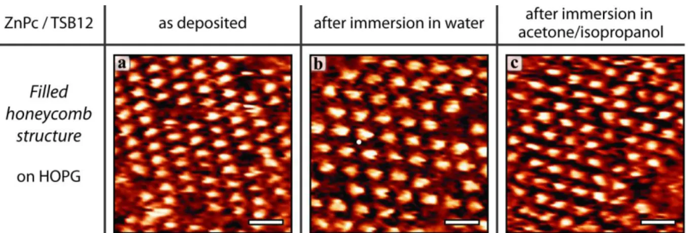
To further demonstrate the versatility of our strategy and the possible functionalization of the vdW heterostructure, we have fabricated the second P2 prototype. Here, we utilize surface-confined supramolecular host–guest chemistry as an approach for the immobilization of a functional guest species, zinc-phthalocyanine (ZnPc, Scheme 2b), in a TSB12-based host template porous monolayer. ZnPC and TSB12 were
Journal XX (XXXX) XXXXXX
Author et al
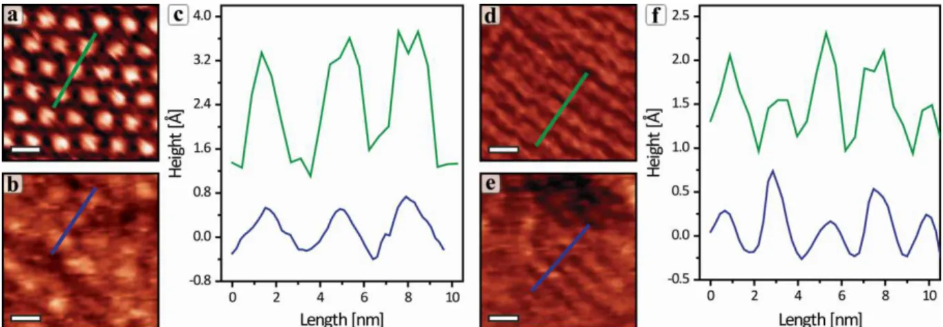
5 Figure 2. Four-component hybrid multilayer vdW heterostructure. (a-c) Schematics and (d-f) STM images of (a,d) bare and (b,e) graphene-covered co-existing dense and ZnPc-filled honeycomb molecular patterns formed by TSB12 molecules directly on HOPG surface, and (c,f) subsequent coverage of this graphene by a second layer of co-deposited ZnPc and TSB12 molecules showing similar assembly. Superimposed: filled hexagonal (i.e. triangular) motif formed from conjugated ZnPc hosts (green spots) Scale bars: (d-f) 10 nm. Tunnelling parameters: (d) 122 pA, 1834 mV, (e) 131 pA, 1828 mV, (f) 166 pA, 1906 mV.
chosen since the guest molecule diameter (~ 1.5 nm) fits within the host porous network cavity (∅=1.9 nm) [20]. To check whether such composite systems are also amenable to the constitution of vdW heterostructures, we transposed the above experiments.
Figure 2 shows that the results fully parallel those obtained with pristine TSB10 molecular units. Thanks to experimental conditions for the host-guest system deposition (See Experimental section and Figure 2a), co-existing dense (linear motifs) and ZnPc-filled honeycomb (triangular motifs) molecular patterns are formed during the first stage of the fabrication process, as evidenced by STM (Figure 2d). Thereafter, we demonstrated the stability of the host-guest system self-assembled on HOPG subjected to immersions into the various aqueous solution and organic solvent baths as well as to thermal treatments required by CDV graphene transfer process (See Experimental section and Figures S6 and S7). Then, the coverage of the previous system with graphene was carried out (Figure 2b). STM analysis of this new layered hybrid heterostructure shows that both triangular and linear motifs are still observable (Figure 2e). However, the large
contrast produced by ZnPc filled pores in honeycomb domains prior to graphene transfer is strongly reduced after graphene coverage (Figure 2d,e and Figure S8a-c), further illustrating the difference between direct resonant STM imaging of the conjugated moieties and indirect one through graphene deformations. The comparison with the sample obtained without any molecular layer, i.e. the same control sample as for P1 (Figure 1 g-i) shows even more pronounced differences. Again, line patterns not present in the control can be ascribed to dense lamella of TSB and numerous defects are observed in triangular patterns ascribed to now ZnPc-filled honeycomb domains. Here, the reduced contrast of the latter shows that ZnPc is only slightly higher than TSB12. The apparent corrugation of graphene cover is ~0.5 Å over lamella (Figure S8 e) that is the same as P1 (Figure S3 e) which is fully consistent since no ZnPc are hosted by these domains. The corrugation of covered ZnPc-filled honeycombs (0.8-1.0 Å, Figure S8 b) remains much lower than the control sample (1-1.5 Å Figure S4b,c). Moreover, the ZnPc-filled honeycomb domains seem to have been more disordered by graphene transfer than pristine TSB10. As concerns the lamella patterns, their geometrical parameters are compatible, within experimental uncertainties, with the dense lattice formed by TSB12 units (Figure 2d,e and Figure S8d-f). These results demonstrate that the stability of adsorbed ZnPcs benefits from the robustness of the TSB12 host matrix. Finally, in the last stage of the heterostructure construction (Figure 2c), the top graphene layer is suitable for the formation of an additional self-assembled molecular monolayer, integrating the ZnPc guest, as demonstrated by STM (Figure 2f).
3. Experimental section
3.1 Chemicals
TSB-Cn (see chemical formula in Scheme 1a, R = CnH2n+1, with n = 10 and 12) were synthesized and purified by adapting the procedure described in the litterature [25] from 3,5-dialkyloxybenzaldehyde. ZnPc (see chemical formula in Scheme 1b) and toluene provided by Sigma-Aldrich with purity 97% (dye content) and 99.8% (anhydrous), respectively, were used as received.
3.2 STM characterization.
Highly oriented pyrolytic graphite (HOPG from SPI supplies, grade 2) was used as a substrate. To obtain atomically clean surfaces the graphite substrate was cleaved with the adhesive tape technique, and subsequently checked by scanning tunnelling microscopy (STM) under air atmosphere condition.
The molecular monolayers were grown on top of HOPG substrate by dropping either i) a 5-µl toluene solution of two similar in structure but different in size molecules from the
6 TSB family, or ii) 5-µl of toluene solution of mixture of TSB and ZnPc molecules.
STM operated in the height mode and air-solid or liquid-solid interfaces. The tips were mechanically fabricated from a 250-µm platinum-iridium wire (Goodfellow, Pt80Ir20).
3.3 Preparation of prototypes P1 and P2.
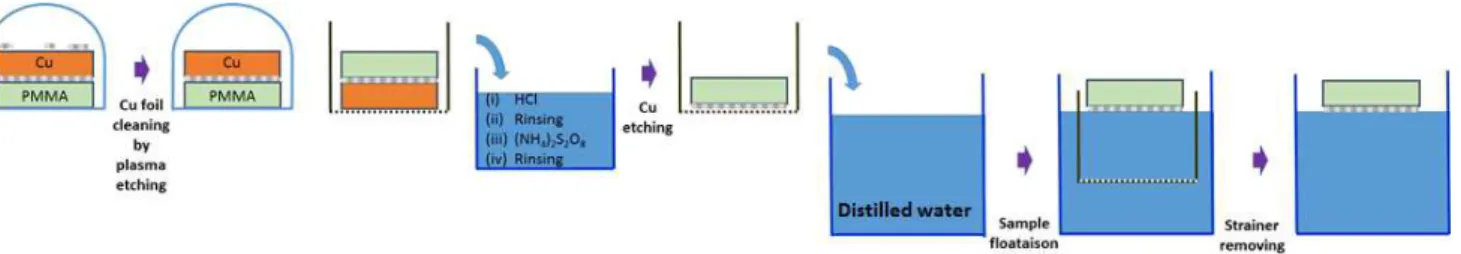
Schemes 1 and S1 summarize the manufacturing process. The 1 × 1 cm2 graphene samples were provided by Graphenea
supplier as single-layer graphene film CVD-grown on a Cu foil with PMMA coating meant to ease the transfer process and to avoid contamination. In order to transfer this graphene onto the HOPG substrate covered by molecules, the following procedure was applied. In order to remove undesirable graphene flakes on the back side of the Cu foil, the sample was placed with copper side facing upwards in a vacuum chamber, and plasma-etched during 30 seconds with a mixture consisting of 95% O2 and 5% Ar. Then, the sample, this time
with PMMA side facing upwards, was shifted to a sterile cell strainer subsequently immersed in solutions of HCl 0,5 M for 10 min and (NH4)2S2O8 0,2 M for 2 hours with aim to finish
the process of cleaning and etching of the Cu foil, respectively. Prior and after Cu etching step, the sample was left floating in bath of distilled water one and three times by 15 min each, respectively, to rinse its surface from earlier used solvents. Then, the strainer containing the graphene/PMMA membrane is entirely immersed in a deep and wide glass crystallizing dish filled with distilled water, and it is gently removed from this reservoir without touching the graphene/PMMA sample floating on the surface of water. The earlier prepared HOPG/molecules substrate held with metal tweezers was dipped into the water next to the graphene under inclination angle of 30°. PMMA-covered graphene membrane is then moved slowly to the substrate by a small water current created with an external microscope glass slide. Once the edge of membrane is in contact with the substrate, the latter is slowly moved from the water under an angle of 30° while the whole graphene will not be attached to its surface. Control experiments reported in figure S2 show that both dense and honeycomb monolayers are imune to immersion into water. To remove the rest of water and improve adhesion of graphene onto the substrate, the sample is left to dry for 30 min in vertical position, and subsequently annealed for 30 min between 60 °C and 100 °C depending on the type of molecules trapped between HOPG and graphene. In fact, we observed a transition from honeycomb to dense structure after annealing of TSBs above 80 °C (Figure S9). This is why we reduced the annealing temperature with respect to the recommended one and increased the annealing duration accordingly. In order to dissolve the PMMA layer on graphene, the sample was left in a glass-crystallizing dish filled with acetone and covered with parafilm overnight. Then, the sample was rinsed with isopropanol for 15 min to remove the PMMA residuals and let
it dry. During the PMMA removal process, the molecular monolayer remains covered by the graphene monolayer which prevents direct contact with the solvents. Notice that even deprived from this graphene cover the molecular layer on HOPG is rather imune to action of acetone and isopropanol (see figure S2). Finally, a second layer of either TSB or a mixture of TSB and ZnPc molecules was deposited on top of the freshly transferred graphene by the same method as the first molecular layer.
Each step of sample preparation was checked with homemade room temperature STM.
4. Conclusions
In conclusion, by combining two van der Waals interactions-based approaches, namely in-plane supramolecular self-assembly and out-of-plane layer-to-layer attractive forces, we have provided a methodology to realize a new class of hybrid multilayer vdW heterostructure through a soft process. Host–guest chemistry in two-dimensional supramolecular porous networks promotes the functionalization of the heterostructure. Arbitrary sequences can be elaborated through the library of available 2D crystals and the versatility of the organic building blocks, e.g. the presence or not (as shown here) and nature [24-25] of guest functional molecules at each level.The demonstration of further self-assembly on top of the stack shows the possible extension of this principle to bulk distributed heterojunctions with record density. Altogether, these results might promote a new paradigm in van der Waals heterostructures of 2D materials.
Acknowledgements
This research was supported by Global Research Laboratory (GRL) through the National Research Foundation of Korea (NRF) funded by the Ministry of Science, ICT & Future Planning (2016K1A1A2912753), by a National Research Foundation (NRF) grant funded by the Korean government (Ministry of Science, ICT & Future Planning,
MSIP) through the Brain Pool program
(2018H1D3A2001751), and by a grant overseen by the French National Research Agency (ANR), project SMAL’LED, ANR-14-CE26-0016. N. K. thanks Dr. Lydia Sosa-Vargas (Sorbonne Université, Institut Parisien de Chimie Moléculaire) for providing TSB derivatives.
References
[1]Geim, A. K.; Grigorieva, I. V. Van der Waals heterostructures.
Nature 2013, 499 (7459), 419-425.
[2]Novoselov, K. S.; Fal'ko, V. I.; Colombo, L.; Gellert, P. R.; Schwab, M. G.; Kim, K. A roadmap for graphene. Nature 2012,
Journal XX (XXXX) XXXXXX
Author et al
7
[3] Novoselov, K. S.; Mishchenko, A.; Carvalho, A.; Neto, A. H. C. 2D materials and van der Waals heterostructures. Science 2016,
353 (6298), aac9439.
[4] Liu, Y.; Weiss, N. O.; Duan, X. D.; Cheng, H. C.; Huang, Y.; Duan, X. F. Van der Waals heterostructures and devices. Nat.
Rev. Mater. 2016, 1 (9), 16042.
[5] Jariwala, D.; Marks, T. J.; Hersam, M. C. Two-dimensional supramolecular self-assembly: nanoporous networks on surfaces. Nature Mater. 2017, 16 (2), 170-181.
[6] Gobbi, M.; Orgiu, E.; Samori, P. When 2D materials meet molecules: Opportunities and challenges of hybrid organic/inorganic van der Waals heterostructures. Adv. Mater. 2018, 30 (18), 1706103.
[7] Lee, C. H. et al. Epitaxial growth of molecular crystals on van der Waals substrates for high-performance organic electronics.
Adv. Mater. 2014, 26 (18), 2812-2817.
[8] He, D. Wet al. Two-dimensional quasi-freestanding molecular crystals for high-performance organic field-effect transistors.
Nat. Commun. 2014, 5, 5162.
[9] Jariwala, D.; Howell, S. L.; Chen, K. S.; Kang, J. M.; Sangwan, V. K.; Filippone, S. A.; Turrisi, R.; Marks, T. J.; Lauhon, L. J.; Hersam, M. C. Hybrid, gate-tunable, van der Waals p-n heterojunctions from pentacene and MoS2. Nano Lett. 2016, 16
(1), 497-503.
[10] Santos, E. J. G.; Scullion, D.; Chu, X. S.; Li, D. O.; Guisinger, N. P.; Wang, Q. H. Rotational superstructure in van der Waals heterostructure of self-assembled C-60 monolayer on the WSe2
surface. Nanoscale 2017, 9 (35), 13245-13256.
[11] Sosa-Vargas, L.; Kim, E.; Attias, A. J. Beyond "decorative'' 2D supramolecular self-assembly: strategies towards functional surfaces for nanotechnology. Mater. Horizons 2017, 4 (4), 570-583.
[12] Cui, D.; MacLeod, J. M.; Rosei, F. Probing functional self-assembled molecular architectures with solution/solid scanning tunnelling microscopy. Chem. Commun. 2018, 54 (75), 10527-10539.
[13] MacLeod, J. M.; Rosei, F. Molecular self-assembly on graphene. Small 2014, 10 (6), 1038-1049.
[14] Mali, K. S.; Greenwood, J.; Adisoejoso, J.; Phillipson, R.; De Feyter, S. Nanostructuring graphene for controlled and reproducible functionalization. Nanoscale 2015, 7 (5), 1566-1585.
[15] Ciesielski, A.; Samori, P. Supramolecular approaches to graphene: From self-assembly to molecule-assisted liquid-phase exfoliation. Adv. Mater. 2016, 28 (29), 6030-6051.
[16] Georgakilas, V.; Otyepka, M.; Bourlinos, A. B.; Chandra, V.; Kim, N.; Kemp, K. C.; Hobza, P.; Zboril, R.; Kim, K. S. Functionalization of graphene: Covalent and non-covalent approaches, derivatives and applications. Chem. Rev. 2012, 112 (11), 6156-6214.
[17] Elemans, J. A. A. W.; Lei, S.; De Feyter, S. Molecular and supramolecular networks on surfaces: from two-dimensional crystal engineering to reactivity. Angew. Chem. Int. Ed. 2009,
48 (40), 7298-7332.
[18] Kudernac, T.; Lei, S.; Elemans, J. A. A. W.; De Feyter, S. Two-dimensional supramolecular self-assembly: nanoporous networks on surfaces. Chem. Soc. Rev. 2009, 38 (2), 402-421. [19] Bléger, D.; Kreher, D.; Mathevet, F.; Attias, A. J.; Schull, G.;
Huard, A.; Douillard, L.; Fiorini-Debuisschert, C.; Charra, F. Surface noncovalent bonding for rational design of hierarchical molecular self-assemblies. Angew. Chem. Int. Ed. 2007, 46 (39), 7404-7407.
[20] Arrigoni, C.; Schull, G.; Bléger, D.; Douillard, L.; Fiorini-Debuisschert, C.; Mathevet, F.; Kreher, D.; Attias, A. J.; Charra,
F. Structure and epitaxial registry on graphite of a series of nanoporous self-assembled molecular monolayers. J. Phys.
Chem. Lett. 2010, 1 (1), 190-194.
[21] Kalashnyk, N.; Jaouen, M.; Fiorini-Debuisschert, C.; Douillard, L.; Attias, A. J.; Charra, F. Electronic effects of the Bernal stacking of graphite on self-assembled aromatic adsorbates.
Chem. Commun. 2018, 54 (69), 9607-9610.
[22] Bellec, A.; Arrigoni, C.; Schull, G.; Douillard, L.; Fiorini-Debuisschert, C.; Mathevet, F.; Kreher, D.; Attias, A. J.; Charra, F. Solution-growth kinetics and thermodynamics of nanoporous self-assembled molecular monolayers. J. Chem. Phys. 2011, 134 (12), 124702.
[23] Schull, G.; Douillard, L.; Fiorini-Debuisschert, C.; Charra, F.; Mathevet, F.; Kreher, D.; Attias, A. J. Single-molecule dynamics in a self-assembled 2D molecular sieve. Nano Lett. 2006, 6 (7), 1360-1363.
[24] Schull, G.; Douillard, L.; Fiorini-Debuisschert, C.; Charra, F.; Mathevet, F.; Kreher, D.; Attias, A. J. Selectivity of single-molecule dynamics in 2D molecular sieves. Adv. Mater. 2006,
18 (22), 2954-2957.
[25] Brisse, R.; Guianvarc'h, D.; Mansuy, C.; Sagan, S.; Kreher, D.; Sosa-Vargas, L.; Hamitouche, L.; Humblot, V.; Arfaoui, I.; Labet, V.; Paris, C.; Petit, C.; Attias, A. J. Probing the in-air growth of large area of 3D functional structures into a 2D supramolecular nanoporous network. Chem. Commun. 2018, 54 (72), 10068-10071.
[26] Vasu, K. S. et al. Van der Waals pressure and its effect on trapped interlayer molecules. Nature Commun. 2016, 7, 12168. [27] Flores, M.; Cisternas, E.; Correa, J. D.; Vargas, P. Moire patterns on STM images of graphite induced by rotations of surface and subsurface layers. Chem. Phys. 2013, 423, 49-54.
1
Functional hybrid multilayered van der Waals heterostructures from graphene and
self-assembled supramolecular 2D crystals
Nataliya Kalashnyk
1,3, Anaïs Gouesmel
1, Eunkyoung Kim
2,4, André-Jean Attias
3,4and Fabrice Charra
11
SPEC, CEA, CNRS, UMR 3680, Université Paris-Saclay, CEA Saclay, 91191 Gif-sur-Yvette Cedex, France
2Department of Chemical and Biomolecular Engineering, Yonsei University, 50 Yonsei-ro, Seodaemun-gu,
Seoul, Korea
3
Institut Parisien de Chimie Moléculaire, UMR CNRS 8232, Sorbonne Université, 4 Place Jussieu, 75252 Paris
Cedex, France
4