Publisher’s version / Version de l'éditeur:
ACS Applied Materials and Interfaces, 10, 7, pp. 6090-6095, 2018-02-05
READ THESE TERMS AND CONDITIONS CAREFULLY BEFORE USING THIS WEBSITE.
https://nrc-publications.canada.ca/eng/copyright
Vous avez des questions? Nous pouvons vous aider. Pour communiquer directement avec un auteur, consultez la
première page de la revue dans laquelle son article a été publié afin de trouver ses coordonnées. Si vous n’arrivez pas à les repérer, communiquez avec nous à [email protected].
Questions? Contact the NRC Publications Archive team at
[email protected]. If you wish to email the authors directly, please see the first page of the publication for their contact information.
NRC Publications Archive
Archives des publications du CNRC
This publication could be one of several versions: author’s original, accepted manuscript or the publisher’s version. / La version de cette publication peut être l’une des suivantes : la version prépublication de l’auteur, la version acceptée du manuscrit ou la version de l’éditeur.
For the publisher’s version, please access the DOI link below./ Pour consulter la version de l’éditeur, utilisez le lien DOI ci-dessous.
https://doi.org/10.1021/acsami.7b19305
Access and use of this website and the material on it are subject to the Terms and Conditions set forth at
Bottom-up, robust graphene ribbon electronics in all-carbon molecular
junctions
Supur, Mustafa; Van Dyck, Colin; Bergren, Adam J.; McCreery, Richard L.
https://publications-cnrc.canada.ca/fra/droits
L’accès à ce site Web et l’utilisation de son contenu sont assujettis aux conditions présentées dans le site LISEZ CES CONDITIONS ATTENTIVEMENT AVANT D’UTILISER CE SITE WEB.
NRC Publications Record / Notice d'Archives des publications de CNRC:
https://nrc-publications.canada.ca/eng/view/object/?id=57487c65-c5c4-41ec-acd4-3a91432847b9 https://publications-cnrc.canada.ca/fra/voir/objet/?id=57487c65-c5c4-41ec-acd4-3a91432847b9Bottom-up, Robust Graphene Ribbon Electronics in All-Carbon
Molecular Junctions
Mustafa Supur,
†Colin Van Dyck,
‡Adam J. Bergren,
‡and Richard L. McCreery
*
,†,‡†
Department of Chemistry, University of Alberta, 11227 Saskatchewan Drive, Edmonton, Alberta T6G 2G2, Canada
‡
National Institute for Nanotechnology (NINT), National Research Council Canada, 11421 Saskatchewan Drive, Edmonton, Alberta T6G 2M9, Canada
*
S Supporting InformationABSTRACT: Large-area molecular electronic junctions consist-ing of 5-carbon wide graphene ribbons (GR) with lengths of 2− 12 nm between carbon electrodes were fabricated by electro-chemical reduction of diazotized 1,8-diaminonaphthalene. Their conductance greatly exceeds that observed for other molecular junctions of similar thicknesses, by a factor of >1 × 10⁴compared to polyphenylenes and >1 × 10⁷compared to alkane chains. The remarkable increase of conductance of the GR nanolayer results from (i) uninterrupted planarity of fused-arene structure affording extensive π-electron delocalization and (ii) enhanced electronic coupling of molecular layer with the carbon bottom contact by two-point covalent bonding, in agreement with DFT-based simulations.
KEYWORDS: molecular electronics, graphene ribbons, molecular junction, electron transport, graphene electronics
M
olecular electronics (ME) entails incorporating single molecules or arrays of molecules into electronic circuits, such that charge transport occurs through the molecules and is sensitive to molecular structure.1,2 ME development was stimulated not only by the possibility of increased device density but also by the prospect of unusual electronic functions not readily achieved with conventional semiconductor technol-ogy.3−6 Key parameters controlling charge transport in MEdevices are the degree of conjugation in the molecular component, the “contact” between a metallic conductor and the molecules, and the distance over which transport must occur to provide a useful function.4−6 Molecular layers of
conjugated aromatic molecules exhibit higher conductivity compared to saturated alkyl substituents in electronic junctions;7,8 however, torsional angles between the singly bonded, freely rotating aromatic rings significantly decrease the π-electron delocalization for long transport distances.9 Single molecule studies of planar, fused ring aromatic molecules in break junctions have shown that conductance and delocaliza-tion can be increased significantly compared to nonplanar aromatic oligomers.10Aside from the progress in fundamental understanding of molecular junctions, the ultimate goal is the integration of molecules into consumer electronics, which has been hindered by both fabrication difficulties and device stability, leading to lifetime and temperature tolerance that is not amenable to broad applications.3−6
Graphene-based materials, particularly graphenic ribbons, represent planar conjugated conductors with high conductiv-ity,11and graphene structures have been used as electrodes in
molecular electronic devices.12On-surface growth of GRs by chemical vapor deposition (CVD), which is the most common technique for GR synthesis and regarded as an efficient method for industry-level production,13 requires catalytic metal substrates and high vacuum and temperature vessels, followed by multistep transfer protocols to target substrates for device construction.14−17 Due in part to the complexity in transfer
procedures,13the use of such graphenic ribbon structures as the components of a molecular electronic junction suspended between the contacts is still challenging.
In this letter, we report large-area molecular electronic junctions of graphene ribbon (GR) nanolayers obtained by electrochemical reduction of a naphthalene double diazonium reagent (Figure 1A) on a flat carbon surface. Our objective was to provide two-point bonding between the naphthalene oligomers and the carbon substrate and formation of a planar, 5-carbon wide GR in the molecular layer. Both the two-point electrode/molecule bond and GR planarity are expected to promote a larger system conductance from a broadening-induced overlap of molecular orbital energies and contact Fermi levels. The “bottom-up”, room-temperature procedure presented in this study avoids the harsh conditions of CVD for graphene synthesis and any transfer methods described for the previously reported GR structures and their electronic devices.13,15 The GRs described in this study grows directly Received: December 20, 2017
Accepted: February 5, 2018 Published: February 5, 2018
Letter www.acsami.org Cite This:ACS Appl. Mater. Interfaces 2018, 10, 6090−6095
on flat sp2-hybridized carbon bottom contacts through covalent bonding with excellent chemical and thermal stability,18 thus providing a “seamless” junction at the contact/molecule interface. A carbon top contact deposited on the GR nanolayer completes the fabrication of GR molecular junction (GRMJ). Lastly, theoretical analysis comparing the electronic behaviors of phenylene oligomers with nonzero dihedral angles and planar ribbons of fused naphthalenes is also presented and correlated with the experimental results.
The fabrication process of the proposed GRMJs is shown in Figure 1. Naphthalene-based GRs of varying length were grown on pyrolyzed photoresist film, (PPF, < 0.5 nm rms roughness) by electrochemical reduction of the double diazonium ion of 1,8-diaminonaphthalene (1,8-DAN,Figure 1A). The diazonium reagent was generated by an in situ process in acetonitrile (ACN) solution of 1,8-DAN by adding tert-butylnitrite (t-buNO2).19 Grafting on patterned PPF was achieved by electrochemical reduction of double diazonium ions of naphthalene, which irreversibly yields N2 and naphthalene Figure 1.(A) Fabrication of GR junctions on patterned PPF: (a) In situ diazotization of diamines of naphthalene building blocks (1,8-DAN) by tert-butylnitrite (t-buNO2) in Ar-bubbled ACN at room temperature, (b) electroreduction of diazonium ions yielding aryl biradical and N2, (c)
successive grafting of generated naphthalene biradicals on PPF and on top of each other yielding GR, and (d) top contact deposition by electron beam deposition of carbon (eC, 10 nm) and gold (30 nm). (B) Photograph of a GRMJ device on Si/SiOxchip. (C) Molecular junctions of singly
bonded layers of TP, BP, and NA generated by electroreduction of their diazonium ions on PPF for comparison with doubly bonded GR (top contact: eC, 10 nm; Au, 30 nm).
Figure 2.(A) Calculated Raman spectrum of GR trimer (i), Raman spectra of GR polymer (ii), 18 nm (iii), 9 nm (iv), 4.2 nm thick GR layers (v), 4.2 nm thick NA layer (vi) on PPF, and calculated Raman spectrum of NA trimer (vii). The intensity scale bar shown for iii also applies to iv−vi. Spectra i and vi were calculated with identical parameters, and i is 30 times more intense than vi. (B) Atomic motions for the 1316 and 1612 cm−1
modes of GR trimer. (C) Absorption spectra of 8.8 nm (i), 4.8 nm (ii), 3.0 nm thick GR layers (iii), 3.2 nm thick NA layer (iv) on optically transparent PPF and naphthalene in ACN (v). Figure A(ii) was adapted with permission from ref23. Copyright 2016 American Chemical Society.
ACS Applied Materials & Interfaces Letter
DOI:10.1021/acsami.7b19305
ACS Appl. Mater. Interfaces 2018, 10, 6090−6095
biradicals, which readily attach to the PPF surface by covalent bonds. Successive electroreduction cycles build the ribbon structures, consisting of fused naphthalene units (Figure 1A). The thickness of GR layer on PPF can be easily controlled by changing the parameters of cyclic electrochemical reduction. Electron-beam deposition of carbon (eC, 10 nm thick) and gold (30 nm) through a shadow mask on the GR-grafted PPF stripes produces the large-area GRMJ (0.00125 cm2) shown in
Figure 1B. MJs made by covalently bonding aromatic molecules to PPF by electrochemical reduction of parent diazonium reagents followed by a top contact of eC and Au have been reported previously,20,21 and were proven to be sufficiently stable and temperature tolerant for a commercial applica-tion.3,20 Figure 1C shows MJs of several oligomers made by electrochemical reduction of diazonium reagents of singly bonded terphenyl (TP), biphenyl (BP), and naphthalene with one amino substituent (NA) for comparison of their conductance with those of GRMJs. Fabrication details for junctions are provided inSupporting Information.
GR films on PPF were characterized by AFM, voltammetry, Raman and UV−vis spectroscopy, often in comparison to PPF modified with oligomers of singly bonded NA. AFM images and line scans for PPF before and after modification with a 5.9 nm thick GR oligomer layer are shown inFigure S2 and S3, and exhibit a small increase in rms roughness from Rq= 0.38 to 0.60 nm. The rms roughness of the PPF/GR surfaces remains below 1 nm for GR thickness up to 12 nm (Table S1).
Structural diagnosis of GR was done by the Raman spectroscopy, which is commonly used for the characterization of graphitic materials.22 Raman spectra of modified PPF/GR and PPF/NA surfaces are shown in Figure 2A after the subtraction of the Raman bands of PPF (Figure S4Ashows the raw spectra). Raman features of GRs on PPF with indicated thicknesses are consistent with those reported for a graphene nanoribbon polymer with the same ribbon backbone23 and exhibit increased intensity with thickness. The Raman spectra reveal typical rylene ribbon (fused naphthalene units) peaks at 1609 and 1327 cm−1, which respectively originate from the
symmetric CC stretches along the long axes of the ribbons and the breathing modes of the central rings between the fused naphthalene units (Figure 2B).24,25 The breathing mode of central rings at 1327 cm−1is a useful diagnostic, because it is strong in both DFT and PPF/GR spectra, but absent in surface enhanced NA/PPF spectrum and in its DFT simulation (Figure S4B). The rigid and planar structure of GRs provides extensive polarizability, permitting observation of Raman features in nanometric films without the need of surface enhancement. In contrast, Raman features for NA [(Figure 2A(vi)], TP and BP on carbon surfaces with d = 1 to 8 nm are undetectable,26 presumably due to nonplanar configurations of singly bonded phenyl rings with unrestrained torsional angles that significantly decrease polarizability.27 DFT calculations predict an approx-imately 30× increase in polarizability for GR compared to NA oligomers (Figure 2A). Possible deviations from linear oligomer structure cause significant decrease in Raman intensity and splitting or broadening of Raman signatures.26 Although the spectra and conductance of the GR films are consistent with the ribbon structure, there may be nonlinear and singly bonded defects which are not observed due to their low Raman cross section and minor contributions to conductance. The consistency of observed, reported and DFT-simulated spectra of GR (Figure 2A) and the approximately linear increase of Raman intensity during the layer growth (Figure S4C) imply that the linear rylene structure is maintained for the 2−12 nm range of layer thickness. GR layers survive during the electron beam deposition of top contact materials (eC and Au) as the same Raman signatures with reduced intensity are observed after deposition of the top contact (Figure S4D).
Figure 2C shows UV−vis spectra for naphthalene in ACN, and for PPF/NA and PPF/GR after subtraction of the PPF absorption (as described inFigure S5). As observed with other aromatic molecules previously,28,29electronic coupling between the π-systems of the chemisorbed molecule and the PPF substrate causes a significant red shift of the onset of absorption. The long wavelength absorption becomes more pronounced with increasing thickness of the GR layer, implying Figure 3.(A−C) JV curves for GR, NA, TP, FL, and nitroazobenzene (NAB) junctions with indicated molecular layer thickness in nanometers. (D) Overlay of JV curves of GR junction (4.6 nm) before and after the 5 million cycles in air at 1000 V/s. Vappis the voltage bias applied across the MJ
while the current was monitored. FL and NAB curves were adapted with permission from ref29. Copyright 2017 American Chemical Society.
that electronic coupling extends over the entire ribbon, at least up to 8.8 nm. Along with the increase in the tail absorption at longer wavelengths, redshift of the absorption maximum from 268 to 288 nm is observed as the thickness of GR layer increases from 3.0 to 8.8 nm. As noted for other aromatic molecules, the increasing red shift is an indication of electronic coupling between molecules in the oligomer.28,29Finally, cyclic voltammetry of ferrocene in ACN solution on PPF/GR and PPF/NA surfaces reveals distinctly different characteristics implying much faster electron transfer through GR than NA (Figure S6).
Current density vs bias voltage (JV) curves are shown in Figure 3for PPF/GR/eC/Au MJs with GR thickness of 5.9 nm compared to those for NA (5.4 nm), TP (4.9 nm), and fluorene (FL, 5.0 nm), obtained in all cases at 1000 V/s in air with device area of 0.00125 cm2. Despite being the thickest of the 4 molecular layers, GR (5.9 nm) has much higher conductance than NA, TP or FL, by a factor of >150 for NA at V = 0.25 V. MJs with thinner GR layers (1.9−5.4 nm,Figure 3B) exhibiting current densities above 10 A/cm2, and conductance approx-imately a factor of 107 larger than that observed for carbon-based alkane junctions.7JV curves for thicker films with d ∼ 8
nm (Figure 3C) confirm the high conductivity of GR compared to other singly bonded aromatic molecules, with J for GR(8.8 nm) exceeding that for TP (7.9 nm) by a factor of >15000 at V = 1.0 V. The high conductance of GR devices is very stable, with minor changes in response apparent after at least 5 million
JV cycles to ±4 A/cm2for a 4.6 nm-thick GR device (Figure 3D and Figure S7). Extension of the GR (4.5 nm) JV curve to higher bias than inFigure 3D demonstrated that GR (7.5 nm) junctions are capable of conduction up to the instrumental limit of ±50 A/cm2without apparent change in JV response.
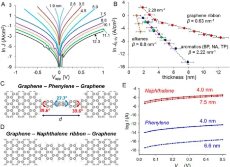
Figure 4A shows ln J vs V curves for a series of GR junctions with d = 1.9−12.3 nm, for which J varies by a factor of more
than 4 orders of magnitude at V = 0.1 V. Figure 4B is an attenuation (i.e., β) plot of ln J(0.1 V) vs d similar to those commonly used to diagnose charge transport mechanisms. The aromatic molecular junctions NA, BP, and TP appear on a single line with slope β = 2.2 ± 0.3 nm−1, similar to the value of 2.7 ± 0.6 nm−1reported for eight aromatic MJs with PPF and Cu contacts.7GR junctions show a similar β below 3.5 nm, but higher J by a factor of ∼25. For d = 3.5−12.3 nm, β is constant at 0.63 ± 0.07 nm−1, resulting in significantly higher conductance than the other aromatics as d increases. At d = 8 nm, the attenuation plots predict a factor of 26 000 higher conductance for GR compared to TP, whereas at d = 12 nm this factor is predicted to be 1.7 × 10⁷. Figure 4B compares attenuation plots for GR at V = 0.5 V, where a range of comparative results are available for other aromatic MJs. The GR junctions have significantly higher conductance than any other molecule yet observed in carbon MJs, including the metal-centered [Ru(bpy)3]2+ case.30A broader comparison is provided by Amdursky et al., who reviewed published results for large-area MJs containing many aliphatic, aromatic, and biological molecular mono- or multilayers in the range of 1−10 nm. For V = 0.1 V and d > 2 nm, the GR conductance exceeds all of the examples cited in this review (Figure S8).31 The change in slope for the GR attenuation plot at d = 3.5 nm (Figure 4B) could have several origins. A transition in charge transport mechanism from coherent tunneling to multistep tunneling29or activated “hopping”,8,32,33has been reported for film thicknesses greater than ∼4 nm. However, the theoretical analysis described next shows that the planar, rigid structure in GR devices yields low attenuation factors for d > 4 nm in the coherent regime without invoking a hopping mechanism.
To further understand the differences between aromatic and GR structures, we carried out state-of-the-art DFT simu-lations,34as described in theSupporting Information. In a first Figure 4.(A) Semilogarithmic scale of JV curves of GR junctions with indicated GR layer thickness in nanometers. (B) Overlay of attenuation plots of GR, NA, TP, BP and alkane junctions with error bars. Alkane data were adapted with permission from ref6. Copyright 2009 Wiley. (C, D) Geometry of a twisted 3-phenylene aromatic chain and a fully conjugated 3-naphthalene ribbon connected to infinite graphene sheets, as computed from ab initio calculations. (E) IV characteristic of a phenylene chain compared to the characteristic of a naphtalene ribbon of similar chain lengths (solid lines). A difference of 7 orders of magnitude is obtained at our level of theory. The decay of conductance obtained for a ribbon is much smaller than the decay obtained for a phenylene, as observable for longer chain lengths characteristics (dashed lines).
ACS Applied Materials & Interfaces Letter
DOI:10.1021/acsami.7b19305
ACS Appl. Mater. Interfaces 2018, 10, 6090−6095
step, the phenylene and GR chains are contacted to infinite graphene electrodes to represent the carbon electrodes, as represented on Figure 4C. The geometries are then relaxed, showing significant dihedral angles at the electrode interface and within the phenylene structures. In comparison, the optimized GR structure is perfectly flat and conjugated, allowing for a seamless contact of the ribbon with sp2 -hybridized electrode. In a second step, we use a Green’s function formalism34 to simulate the IV curves of junctions having different lengths, as reported in Figure 4D. The conductance of the ribbon junction is predicted to be 7 orders of magnitude larger than the phenylene chain with same length. An extension of the ribbon by 3.5 nm results in a minor conductance reduction (β = 0.23 nm−1), while an extension of the phenylene chain by 2.6 nm reduces the current by 3 to 4 orders of magnitude (β = 3.06 nm−1). The small tunneling decay is expected from theory as the infinite GR chain possesses a HOMO−LUMO gap of 0.32 eV at our level of theory. Simulations are in good qualitative agreement with measurements, showing a striking difference between a ribbon and an aromatic conjugated chain. While we do not expect the idealized structures of Figure 4 to correspond closely to the actual device structure, the theory correctly predicts a large difference in β and current density for the GR devices compared to phenylene oligomer.
In summary, variable thickness molecular nanolayers with extensively planar geometry were obtained by electrochemical deposition of naphthalene units on carbon electrodes through two-point covalent bonding. “Bottom-up” deposition by electrochemical reduction of diazonium reagents on a carbon substrate provides a process-friendly route to molecular junctions which is amenable to massively parallel fabrication without material transfer steps. The fabricated GR junctions withstand >1 × 10⁶JV cycles and current densities orders of magnitude higher than reported devices containing nonplanar aromatic oligomers of similar length. Raman and UV−vis spectroscopy, voltammetry, and theoretical analysis are all consistent with extensive planar conjugation through the naphthalene-derived GR layer. The high conductance of GRMJs is a consequence of strong electronic coupling with the carbon contacts and enhanced conjugation in the GR layer. The GRMJ behaves as a robust, extensively conjugated electronic system approaching the behavior of a “molecular short circuit” with electronic coupling extending across the entire carbon/ribbon/carbon structure.
■
ASSOCIATED CONTENT*
S Supporting InformationThe Supporting Information is available free of charge on the ACS Publications websiteat DOI:10.1021/acsami.7b19305.
AFM images, additional Raman and UV−vis−NIR spectra, cyclic voltammograms, additional IV plots, and further details for experiments and theoretical calcu-lations (PDF)
■
AUTHOR INFORMATIONCorresponding Author
*E-mail: [email protected].Tel.: 780-641-1760. ORCID
Mustafa Supur: 0000-0003-2086-7106 Colin Van Dyck: 0000-0003-2853-3821 Richard L. McCreery:0000-0002-1320-4331
Notes
The authors declare no competing financial interest.
■
ACKNOWLEDGMENTSThis work was supported by the University of Alberta, the National Research Council of Canada, the National Sciences and Engineering Research Council, and Alberta Innovates. We acknowledge the computational resources of the Center for Nanoscale Materials (Argonne National Lab), an Office of Science user facility, supported by the U.S. Department of Energy, Office of Science, Office of Basic Energy Sciences, under Contract DE-AC02-06CH11357.
■
REFERENCES(1) Quinn, J. R.; Foss, F. W.; Venkataraman, L.; Hybertsen, M. S.; Breslow, R. Single-Molecule Junction Conductance through Diami-noacenes. J. Am. Chem. Soc. 2007, 129, 6714−6715.
(2) Kim, W. Y.; Kim, K. S. Tuning Molecular Orbitals in Molecular Electronics and Spintronics. Acc. Chem. Res. 2010, 43, 111−120.
(3) Peplow, M. Rebooting the Molecular Computer. ACS Cent. Sci. 2016, 2, 874−877.
(4) Vilan, A.; Aswal, D.; Cahen, D. Large-Area, Ensemble Molecular Electronics: Motivation and Challenges. Chem. Rev. 2017, 117, 4248− 4286.
(5) Jeong, H.; Kim, D.; Xiang, D.; Lee, T. High-Yield Functional Molecular Electronic Devices. ACS Nano 2017, 11, 6511−6548.
(6) McCreery, R. L.; Bergren, A. J. Progress with Molecular Electronic Junctions: Meeting Experimental Challenges in Design and Fabrication. Adv. Mater. 2009, 21, 4303−4322.
(7) Sayed, S. Y.; Fereiro, J. A.; Yan, H.; McCreery, R. L.; Bergren, A. J. Charge Transport in Molecular Electronic Junctions: Compression of the Molecular Tunnel Barrier in the Strong Coupling Regime. Proc.
Natl. Acad. Sci. U. S. A. 2012, 109, 11498−11503.
(8) Taherinia, D.; Smith, C. E.; Ghosh, S.; Odoh, S. O.; Balhorn, L.; Gagliardi, L.; Cramer, C. J.; Frisbie, C. D. Charge Transport in 4 nm Molecular Wires with Interrupted Conjugation: Combined Exper-imental and Computational Evidence for Thermally Assisted Polaron Tunneling. ACS Nano 2016, 10, 4372−4383.
(9) Fraind, A. M.; Sini, G.; Risko, C.; Ryzhkov, L. R.; Brédas, J.-L.; Tovar, J. D. Charge Delocalization through Benzene, Naphthalene, and Anthracene Bridges in π-Conjugated Oligomers: An Experimental and Quantum Chemical Study. J. Phys. Chem. B 2013, 117, 6304− 6317.
(10) Sedghi, G.; Sawada, K.; Esdaile, L. J.; Hoffmann, M.; Anderson, H. L.; Bethell, D.; Haiss, W.; Higgins, S. J.; Nichols, R. J. Single Molecule Conductance of Porphyrin Wires with Ultralow Attenuation.
J. Am. Chem. Soc. 2008, 130, 8582−8583.
(11) Chen, F.; Tao, N. J. Electron Transport in Single Molecules: From Benzene to Graphene. Acc. Chem. Res. 2009, 42, 429−438.
(12) Jia, C.; Ma, B.; Xin, N.; Guo, X. Carbon Electrode−Molecule Junctions: A Reliable Platform for Molecular Electronics. Acc. Chem.
Res. 2015, 48, 2565−2575.
(13) Chen, Y.; Gong, X.-L.; Gai, J.-G. Progress and Challenges in Transfer of Large-Area Graphene Films. Adv. Sci. 2016, 3, 1500343.
(14) Cai, J.; Ruffieux, P.; Jaafar, R.; Bieri, M.; Braun, T.; Blankenburg, S.; Muoth, M.; Seitsonen, A. P.; Saleh, M.; Feng, X.; Mullen, K.; Fasel, R. Atomically Precise Bottom-Up Fabrication of Graphene Nanorib-bons. Nature 2010, 466, 470−473.
(15) Sakaguchi, H.; Kawagoe, Y.; Hirano, Y.; Iruka, T.; Yano, M.; Nakae, T. Width-Controlled Sub-Nanometer Graphene Nanoribbon Films Synthesized by Radical-Polymerized Chemical Vapor Deposi-tion. Adv. Mater. 2014, 26, 4134−4138.
(16) Kimouche, A.; Ervasti, M. M.; Drost, R.; Halonen, S.; Harju, A.; Joensuu, P. M.; Sainio, J.; Liljeroth, P. Ultra-Narrow Metallic Armchair Graphene Nanoribbons. Nat. Commun. 2015, 6, 10177.
(17) Zhang, H.; Lin, H.; Sun, K.; Chen, L.; Zagranyarski, Y.; Aghdassi, N.; Duhm, S.; Li, Q.; Zhong, D.; Li, Y.; Mullen, K.; Fuchs,
H.; Chi, L. On-Surface Synthesis of Rylene-Type Graphene Nanorib-bons. J. Am. Chem. Soc. 2015, 137, 4022−4025.
(18) Mahmoud, A. M.; Bergren, A. J.; Pekas, N.; McCreery, R. L. Towards Integrated Molecular Electronic Devices: Characterization of Molecular Layer Integrity During Fabrication Processes. Adv. Funct.
Mater. 2011, 21, 2273−2281.
(19) Stockhausen, V.; Trippé-Allard, G.; Van Quynh, N.; Ghilane, J.; Lacroix, J.-C. Grafting π-Conjugated Oligomers Incorporating 3,4-Ethylenedioxythiophene (EDOT) and Thiophene Units on Surfaces by Diazonium Electroreduction. J. Phys. Chem. C 2015, 119, 19218− 19227.
(20) Bergren, A. J.; Zeer-Wanklyn, L.; Semple, M.; Pekas, N.; Szeto, B.; McCreery, R. L. Musical Molecules: The Molecular Junction as an Active Component in Audio Distortion Circuits. J. Phys.: Condens.
Matter 2016, 28, 094011.
(21) Bayat, A.; Lacroix, J.-C.; McCreery, R. L. Control of Electronic Symmetry and Rectification through Energy Level Variations in Bilayer Molecular Junctions. J. Am. Chem. Soc. 2016, 138, 12287−12296.
(22) McCreery, R. L. Advanced Carbon Electrode Materials for Molecular Electrochemistry. Chem. Rev. 2008, 108, 2646−2687.
(23) Yang, W.; Lucotti, A.; Tommasini, M.; Chalifoux, W. A. Bottom-Up Synthesis of Soluble and Narrow Graphene Nanoribbons Using Alkyne Benzannulations. J. Am. Chem. Soc. 2016, 138, 9137−9144.
(24) Castiglioni, C.; Mapelli, C.; Negri, F.; Zerbi, G. Origin of the D Line in the Raman Spectrum of Graphite: A Study Based on Raman Frequencies and Intensities of Polycyclic Aromatic Hydrocarbon Molecules. J. Chem. Phys. 2001, 114, 963−974.
(25) Negri, F.; Castiglioni, C.; Tommasini, M.; Zerbi, G. A Computational Study of the Raman Spectra of Large Polycyclic Aromatic Hydrocarbons: Toward Molecularly Defined Subunits of Graphite. J. Phys. Chem. A 2002, 106, 3306−3317.
(26) Supur, M.; Smith, S. R.; McCreery, R. L. Characterization of Growth Patterns of Nanoscale Organic Films on Carbon Electrodes by Surface Enhanced Raman Spectroscopy. Anal. Chem. 2017, 89, 6463− 6471.
(27) Rumi, M.; Zerbi, G. Conformational Dependence of Linear and Nonlinear molecular Optical Properties by Ab Initio Methods: The Case of Oligo-p-phenylenes. Chem. Phys. 1999, 242, 123−140.
(28) Choi, S. H.; Risko, C.; Delgado, M. C. R.; Kim, B.; Bredas, J.-L.; Frisbie, C. D. Transition from Tunneling to Hopping Transport in Long, Conjugated Oligo-imine Wires Connected to Metals. J. Am.
Chem. Soc. 2010, 132, 4358−4368.
(29) Morteza Najarian, A.; McCreery, R. L. Structure Controlled Long-Range Sequential Tunneling in Carbon-Based Molecular Junctions. ACS Nano 2017, 11, 3542−3552.
(30) Tefashe, U. M.; Nguyen, Q. V.; Lafolet, F.; Lacroix, J.-C.; McCreery, R. L. Robust Bipolar Light Emission and Charge Transport in Symmetric Molecular Junctions. J. Am. Chem. Soc. 2017, 139, 7436− 7439.
(31) Amdursky, N.; Marchak, D.; Sepunaru, L.; Pecht, I.; Sheves, M.; Cahen, D. Electronic Transport via Proteins. Adv. Mater. 2014, 26, 7142−7161.
(32) Luo, L.; Balhorn, L.; Vlaisavljevich, B.; Ma, D.; Gagliardi, L.; Frisbie, C. D. Hopping Transport and Rectifying Behavior in Long Donor−Acceptor Molecular Wires. J. Phys. Chem. C 2014, 118, 26485−26497.
(33) Ho Choi, S.; Kim, B.; Frisbie, C. D. Electrical Resistance of Long Conjugated Molecular Wires. Science 2008, 320, 1482−1486.
(34) Brandbyge, M.; Mozos, J.-L.; Ordejón, P.; Taylor, J.; Stokbro, K. Density-functional method for nonequilibrium electron transport.
Phys. Rev. B: Condens. Matter Mater. Phys. 2002, 65, 165401.
ACS Applied Materials & Interfaces Letter
DOI:10.1021/acsami.7b19305
ACS Appl. Mater. Interfaces 2018, 10, 6090−6095