Supporting Information: Evaluating the Use of Edge Detection in
Extracting Feature Size from Scanning Electrochemical Microscopy
Images
Lisa I. Stephens,1 Nicholas A. Payne,1 Sebastian A. Skaanvik,1 David Polcari,1
Matthias Geissler,2 Janine Mauzeroll1∗
1 Department of Chemistry, McGill University, Montreal, QC H3A 0B8, Canada 2 Life Sciences Division, National Research Council of Canada, 75 de Mortagne Boulevard,
Boucherville, QC J4B 6Y4, Canada
* Email: janine.mauzeroll@mcgill.ca
* Phone: +1 514 398 3898
Table of Contents
1 Electrochemical Setup S-2
2 Finite Element Model S-3
3 Enlarged Second Derivatives S-4
4 Atomic Force Microscopy S-5
5 Asymmetrical Reactive Features S-6
6 Accuracy and Feature Size S-7
1
Electrochemical Setup
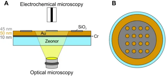
Au/SiO2 substrates were designed to be transparent to allow for simultaneous SECM and
optical imaging (Figure S1). Optical images acquired immediately following the SECM raster
scan were used to align the two images.
Figure S1: Schematic of the integrated electrochemical/optical microscope used to image the Au/SiO2 substrates. (A) Side view. (B) Top view.
2
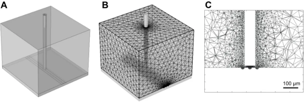
Finite Element Model
A 3D finite element model was built in COMSOL Multiphysics 5.3a with the Transport of
Diluted Species module. This was used to solve the steady-state Nernst Planck equation
under conditions of negligible convection and migration, with the boundary conditions
described previously.(1) The position of the electrode was parameterized enabling SECM
images to be calculated according to a parametric sweep.
An electrolyte domain of 100a× 100a× 80a (x×y×z) was simulated, where a is the radius
of the microelectrode. For both topographical and reactive features, the feature spanned the
entire width of the substrate. An electrode with radius 12.5 µm and RG = 3 was used for
all simulations.
A dense mesh was introduced to the domain with maximum size restrictions applied to
the electrode and feature surfaces of 0.1a and 0.5a (Figure S2) and maximum growth rate
of 1.3 in the electrolyte domain. On average, this produced a final mesh with in excess of
300 000 elements.
Figure S2: (A) Simulation geometry used for the groove simulations. (B) Meshed geometry. (C) Cross-section of the meshed geometry.
3
Enlarged Second Derivatives
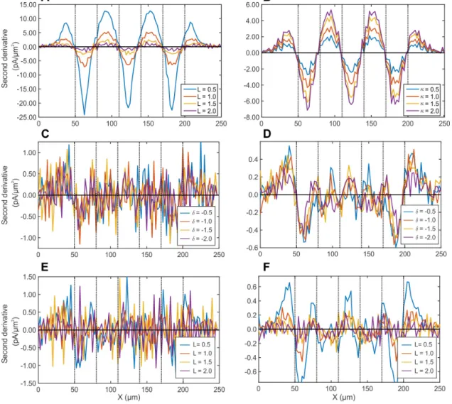
For easier viewing, enlarged versions of the second derivative plots from the main manuscript
have been included below. These were numerically calculated from simulated 1D line scans
over reactive (Figure S3 A-B) or topographical (Figure S3 C-F) features. Zero-crossings of
the second derivative indicate inflection points, dotted lines indicate the true feature edge.
Figure S3: Enlarged versions of the second derivatives plotted in the main manuscript. (A,B) Figure 1 (B,C) respectively. (C,D) Figure 3 (C,D) respectively. (E,F) Figure 3 (F,G) respectively. Dotted lines indicate the true feature edges.
4
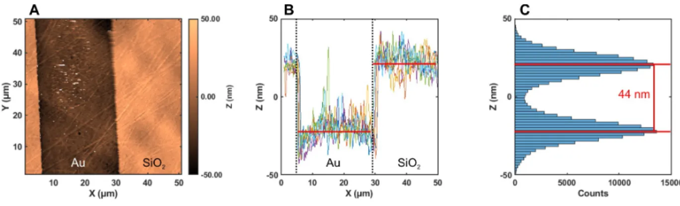
Atomic Force Microscopy
AFM data was collected on a MFP3D-SA atomic force microscope equipped with a 3D
molecular force probe controller (Asylum Research, Santa Barbara, CA, USA). Experiments
were performed in intermittent contact mode in air, using an OPUS 160AC-NA tip (MikroMash,
Sofia, Bulgaria) with a nominal spring constant of 26 N/m, frequency of 300 kHz, and radius
of contact <7 nm.
Figure S4: (A) AFM topography image of the Au/SiO2 interface. (B) Selected line scans
from the AFM image. (C) Histogram of all data to extract the average thickness of the SiO2
5
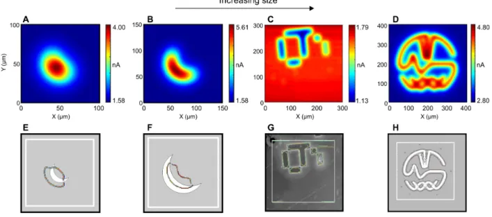
Asymmetrical Reactive Features
To examine the effect of feature symmetry on method accuracy, edge detection was performed
on both simulated (Figure S5 A,B,D) and experimental (Figure S5 C) SECM images. For the
the two moons of different size (Figure S5 A,B), accuracy improves as the feature becomes
larger relative to the electrode size, with the concave shape better represented, though
accuracy is still not optimal at this scale. As the features become even larger (Figure S5
C,D), improved agreement between the detected edges and true feature geometry is observed.
Figure S5: Edge detection on SECM images of asymmetrical reactive features. (A-B) Simulated image of a half moon feature (A) similar in size (B) larger than the electrode. (C) Experimental image of a number 6 (tilted sideways to the right-hand side). (D) Simulated image of our research group logo. (E-H) Detected edges in the SECM image (indicated by the frame in white) overlaid on the corresponding image of the true geometry determined through either (E,F,H) the simulation geometry or (G) a microscope image.
6
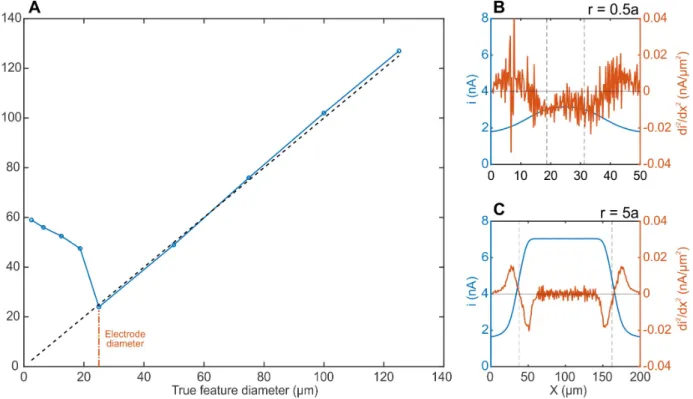
Accuracy and Feature Size
To examine the effect of feature size on method accuracy, edge detection was performed
on simulated linescans over reactive circles of varying size. Optimal accuracy is observed,
measured as agreement between the estimated feature diameter calculated from the detected
edges and true feature diameter input into the simulation, for features the same size as
the electrode or larger. For features smaller than this criteria, edge detection tends to
overestimate the feature size.
Figure S6: (A) The estimated feature size calculated from edge detection compared to the true feature size input into the simulation. (B,C) Raw currents and second derivatives for a simulated line scan over a circular feature with a radius of (B) 0.5a and (C) 5a. Dotted lines indicate the true feature edges.
7
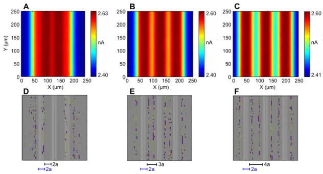
Effect of Groove Spacing
The relationship between feature spacing and edge detection accuracy of topographically
varying substrates was examined by simulating three nonreactive grooves a variable distance
apart (Figure S7). In general, the algorithm tends to miss fewer edges (false negatives) as
the features become further apart, but still tends to overestimate the true feature edges.
Figure S7: Comparison of the edge detection effectiveness for three grooves of the same depth separated by different distances. (A-C) Simulated SECM images for three identical grooves of depth a. (D-F) Edges detected in the SECM images overlaid on the true model geometry employed.
8
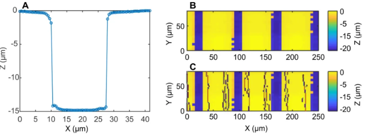
Scanning Ion Conductance Microscopy
Scanning ion conductance microscopy (SICM) was performed to confirm the groove depth
(Figure S8 A) and spacing (Figure S8 B) of the topographically-variant non-reactive Si/SU-8
substrate. Pipettes were pulled from borosilicate glass capillaries (o.d. 1.2 mm and i.d. 0.69
mm) to a tip diameter of 1 µm using a Sutter 2000 pipette puller (Figure S1).(2) A 250
µm diameter Ag/AgCl wire (≥99.99%, Sigma) was used as the working electrode while a
1 mm diameter Ag/AgCl wire (annealed 99.99% Ag wire, Goodfellow) was used as QRCE.
Measurements were carried out in 0.1 M KCl solution.
Table S1: Pipette pulling parameters.
Heat Fil Vel Del Pul Line 1 350 3 40 220 -Line 2 350 3 40 180 100
Scanning ion conductance microscopy was performed using a DC hopping mode approach
with a HEKA ELP-3 system. The probe was manually positioned within 100 µm of the
surface and translated towards the surface at a speed of 10 µm/s with sample interval of 10
nm while applying a voltage of 400 mV between the two Ag/AgCl electrodes. The probe
movement was halted when a current change of 400 pA was observed (approx. 1% of bulk).
The motor position was recorded and the probe was retracted by 20 µm before moving to a
new location.
When the detected edges of the SECM image (Figure 4 A) are overlaid on the SICM map,
Figure S8: A) Line scan over a groove from the SICM image. (B) SICM map of the Si/SU-8 substrate. (C) Detected edges from a representative area of the SECM image overlaid on the SICM map.
9
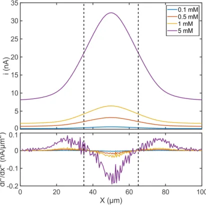
Effect of Mediator Concentration
The effect of bulk mediator concentration on method performance was examined by simulating
line scans over a reactive feature with different bulk concentrations. Provided a sufficiently
high concentration giving a distinct signal is used, the apparent inflection point does not
vary with increasing concentration and correlates well with the true feature edge.
Figure S9: Simulated line scans over the center of a 30 µm radius circular reactive feature at varying initial concentrations of the redox mediator. Dotted lines indicate the true feature edge.
References
[1] Stephens, L. I.; Mauzeroll, J. Analytical Chemistry 2018, 90, 6796–6803.