HAL Id: cea-01573215
https://hal-cea.archives-ouvertes.fr/cea-01573215
Submitted on 8 Aug 2017HAL is a multi-disciplinary open access
archive for the deposit and dissemination of sci-entific research documents, whether they are pub-lished or not. The documents may come from teaching and research institutions in France or abroad, or from public or private research centers.
L’archive ouverte pluridisciplinaire HAL, est destinée au dépôt et à la diffusion de documents scientifiques de niveau recherche, publiés ou non, émanant des établissements d’enseignement et de recherche français ou étrangers, des laboratoires publics ou privés.
Distributed under a Creative Commons Attribution - NonCommercial| 4.0 International License
Electronic Transport of MoS2 Monolayered Flakes
Investigated by Scanning Electrochemical Microscopy
Olivier Henrotte, Thomas Bottein, Hugo Casademont, Kevin Jaouen,
Tiphaine Bourgeteau, Stephane Campidelli, Vincent Derycke, Bruno
Jousselme, Renaud Cornut
To cite this version:
Olivier Henrotte, Thomas Bottein, Hugo Casademont, Kevin Jaouen, Tiphaine Bourgeteau, et al.. Electronic Transport of MoS2 Monolayered Flakes Investigated by Scanning Electrochemical Mi-croscopy. ChemPhysChem, Wiley-VCH Verlag, 2017, 18, pp.2777-2781. �10.1002/cphc.201700343�. �cea-01573215�
1
Electronic transport of MoS
2
monolayered flakes
investigated
by scanning electrochemical microscopy
O. Henrotte, T. Bottein, H. Casademont, K. Jaouen, T. Bourgeteau, S. Campidelli, V. Derycke, B. Jousselme, R. Cornut*
LICSEN, NIMBE, CEA, CNRS, Université Paris-Saclay, CEA Saclay 91191 Gif-sur-Yvette Cedex, France. E-mail: renaud.cornut@cea.fr
Keywords: SECM, CVD MoS2, electronic conduction, modelling
Abstract: The amazing properties of 2D materials are envisioned to revolutionize several domains
such as flexible electronics, electrocatalysis, or biosensing. Herein we introduce Scanning Electrochemical Microscopy (SECM) as a tool to investigate molybdenum disulfide in a straightforward fashion, providing localized information regarding the electronic transport within CVD-grown crystalline MoS2 single layers having micrometric sizes. Our investigations show that
within flakes assemblies some flakes are well electrically interconnected, with no detectable contact resistance, while others are not electrically connected at all independently from the size of the physical contact between them. Overall, the work shows for the first time how the complex electronic behavior of MoS2 flake assemblies (semiconducting nature, contact quality between flakes) can be investigated
with SECM.
2D materials such as graphene, graphene oxide, phosphorene, boron nitride monolayers or transition-metal dichalcogenides (TMDCs) are the subject of increasing attention from the scientific community.[1-2] These materials exhibit appealing characteristics, different from their bulk parents, particularly regarding the transport of charges within these materials. Thus, they are envisioned to be key players in various domains such as flexible electronics, electrocatalysis, or biosensors.
Among 2D transition-metal dichalcogenides (TMDCs) materials, monolayer MoS2 -a direct bandgap
semiconductor- has a special place in the recent literature notably because its optical and electronic properties are very specific to the monolayer form. Its synthesis by chemical vapor deposition (CVD)[3] is rapidly spreading, making high-quality material available to a growing community of physicists, chemists and electrical engineers. However, the extreme thinness (3 atom-thick) of MoS2
and its sensitivity to small variations in the growth parameters result in unavoidable inhomogeneities such as defects, differences in domain shapes, non-perfect Mo/S stoichiometry, etc. Theses variations are likely to have a strong impact on the electronic properties.[4-5] Investigating the consequences of non-idealities would provide helpful insight into MoS2 monolayers, and would further help in finding
the best synthesis and processing conditions. Herein we introduce Scanning Electrochemical Microscopy (SECM) as a tool to investigate TMDCs monolayers in a straightforward fashion, providing localized information regarding the electronic transport within crystalline single-layers of MoS2. It is worth mentioning that to the best of our knowledge, this is the first time that MoS2 flakes
2
Scanning Electrochemical Microscopy consists in scanning close to the surface a micro or a nano-electrode immersed in an electrolyte.[6-7] It provides electrochemical images of the investigated substrate. This technique is particularly suitable to investigate the local electrochemical properties of 2D materials.The versatility of the technique is perfectly matching the diversity of the 2D materials. [8-9] As an illustration, we showed on reduced graphene oxide (rGO) flakes that SECM is very powerful to study without contact the local conductivity of 2D nanomaterials.[10-12] It has also been recently used to investigate the electrocatalytic properties of MoS2 toward Hydrogen evolution
reaction.[13-14] Herein, we focus on the ability of MoS2 to transport electric charges. Using SECM in
the so called feedback mode[15] we show how the electronic conductivity can be locally investigated without contact and directly on the insulating growth substrate avoiding any artefact or contamination arising from post-synthesis processing.
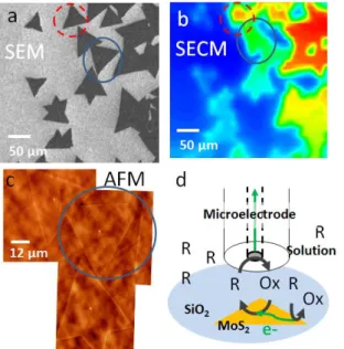
Figure 1 shows the combination of SEM, AFM and SECM images taken on the same area containing CVD MoS2 flakes. Experimental details (CVD-synthesis, SECM imaging, etc.) are provided in the
Supporting Information section. The physicochemical principle associated to each technique permits to obtain information of different nature on the same sample. The SEM image (figure 1a) allows the localization of the flakes and the image contrast confirms the conductive nature of the flakes compared to the substrate. The AFM (figure 1c) provides information regarding the topography of the flakes: thickness and roughness confirm the monolayered nature of the flakes, and inform on the quality of the synthesis. SECM (figure 1b) carries the signature of the local conductivity of the sample, when immersed in an electrolytic solution: the presence of a conductive area underneath the probe enables a feedback loopthat leads to a probe current enhancement. As shown figure 1d, the species consumed at the probe (R) are regenerated at the substrate, thanks to electrons brought by a counter reaction occurring at the substrate, far from the microelectrode. This feedback loop does not occur if the substrate is non-conductive. This phenomenon has similarities with what is encountered in bipolar electrochemistry and in galvanic corrosion, and has been extensively used in previous works to investigate lateral conduction with SECM.[10,16-17] The multistep process associated to the SECM measurement offers many possibilities of investigation as detailed in the following.
For SECM imaging, it must be noticed that the most conventional approach –i.e. use of ferrocene (Fc) as redox mediator- does not permit to obtain stable feedback currents, contrary to what is obtained with decamethylferrocene (dmFc), as presented for example in figure 1b. This observation is in accordance with the fact that MoS2 is an n-type semiconductor: dmFc has a lower redox potential (E ≈
-0.3V vs Ag/AgNO3) than Fc (E ≈ 0.3V vs Ag/AgNO3). In order to further investigate this aspect,
Figure 1. Combined imaging of MoS2 by (a)
SEM, (b) SECM using dmFc 4mM as redox mediator. Red color: 9 nA Blue color: 2.2 nA. Probe radius (rT) 5 microns. (c) AFM showing a
thickness of flakes equal to 0.7 nm, as expected for a monolayer of MoS2 (d) Scheme presenting
the processes involved in the SECM measurement to provide enhance probe signal: the MoS2 layer
is undergoing both an oxidation and a reduction process (and electronic transport between the two reaction locations).
3
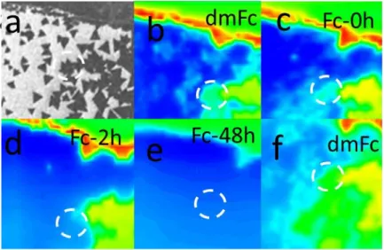
figure 2a and 2b-f show respectively SEM and SECM images obtained in different conditions. Figure 2b was acquired with dmFc, and the response is stable with time. Figure 2c-e shows the SECM responses vs. time when dmFc is replaced by Fc. The SECM images were obtained immediately after removing dmFc and exposing the substrate to Fc (figure 2c), after an immersion of 2h into the Fc solution (Figure 2d), and after an immersion of 48h (Figure 2e). We observe a decrease of the electrochemical response upon exposure to the Fc solution. This instability is the signature of the progressive decrease of the conductivity of the sample, which likely comes from the progressive undoping of the sample in the presence of Fc. First, this proves that the preliminar exposition to dmFc has a doping effect on MoS2 -similarly to what is obtained with other organic reducers studied in
transistor devices.[18] Then, the fact that the undoping process is not immediate -with a significant SECM response observed with Fc after an immersion of 2h may be due to charge traps within SiO2
support, as observed in the literature. [8,19] Notably, the extinction seems faster on small area. This may either come from a higher ability of the grain boundaries to evacuate the charges trapped within SiO2, from a higher ability of large area to dilute charges, or from a higher response at the beginning
of the process of the large area. Further specific investigations are required to discriminate between the different possibilities. In any case, the doping-undoping process is fully reversible, as proven by figure 2f, that shows the immediate recovery of the SECM response after exposure of the inactive sample to dmFc.
Figure 2. (a) SEM image of CVD-grown MoS2 monolayer. (b-f) successive SECM images of the same
area presenting the probe current: (b) with dmFc, (c) with Fc, just after replacing the dmFc solution by the Fc solution (d) with Fc after 2 hours of immersion in the Fc solution (e) with Fc after 48 hours of immersion in the Fc solution, and, finally (f) with dmFc after 48 hours of immersion in the Fc solution. Experimental conditions: dTip = 7 microns. [Mediator] = 1 mM, rT = 5 microns. For each
SECM image, the color scale has been chosen to have negative feedback in blue and the current measured far from sample (Iinf) in green. The red color corresponds to about 150% from Iinf.
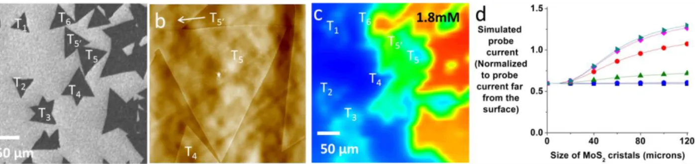
In the next step we investigate in detail specific zones in order to compare the observation with numerical simulations. The results presented in figure 3 show concordant SEM (figure 3a) and SECM (figure 3c) images obtained with dmFc. Figure 3b presents an AFM image of a fraction of this area, confirming the monolayered nature of the investigated flakes.
4
Figure 3. (a) SEM image of CVD-grown MoS2 monolayer (b) AFM image of a MoS2 triangle. (c)
SECM image of the same area as imaged with SEM figure 2(a). Experimental condition: probe substrate distance = 7 µm, [dmFc] = 1.8mM, probe radius = 5 µm. The blue and red color corresponds to 60% and 150% of the probe current measured far from the sample (Iinf), respectively.
(d) Simulations of the probe current as a function of the flake size, for different resistances, from 50 to 5.107 kOhms (1 decade between each curve) ([dmFc] = 1.8mM, dtip=5µm).
Figure 3c shows that the SECM response level is not the same for all the flakes: some flakes have a low response (in green on the SECM image) –corresponding to less than 100% of the probe current measured far from the sample (Iinf) while others have a high response (in yellow and red –
corresponding to more than 100% of Iinf). In fact, the SECM response in the conduction sensing mode
is not only depending on the conductivity underneath the probe, but also on the surrounding’s conductivity. To illustrate this, figure 3d shows numerical simulations obtained for different conductivities, presenting the probe current as a function of the size of the crystal. These simulations were performed using the software COMSOL version 4.3a with a set of equations (presented in section S4 of the Supporting Information) adapted from those developed for our previous studies on reduced graphene oxide flakes.[10-11] At high substrate resistance (curves with black squares and blue circles), whatever the size of the flake, the feedback response is close to the current measured above a pure insulating area, approximately equal to 0.6Iinf. At lower resistance, the larger the
conducting area, the higher the response. This is due to transport limitation of the reactant consumed by the counter reaction occurring at the substrate,[10,20] and explains why the triangles T1 T2, T3 and
T4 –which have increasing sizes- have increasing SECM response levels. This also explains why the
centers of the flakes in figure 1b appear less active: when put in the center of the flake, the probe totally covers the flake, hindering maximally the transport of species reacting at the center. This phenomena is influenced both by the size of the active part of the probe and by the surrounding glass thickness, as discussed in a previous work.[10] Regarding T5 and T5’, they have a higher response
level than T4 because they are well connected through a physical contact as imaged by AFM in figure
3b and by SEM in figure 4a. The flake T6 has the highest feedback response, despite a relative small
5
Figure 4. (a) SEM image of CVD-grown MoS2 monolayer. The arrow indicates the connection area
between the 2 flakes, responsible for the high SECM response of flake T6. (b) and (c) SECM images of
the same area as in figure 1, with different dmFc redox mediator concentrations: (b) 0.3mM (c) 16mM. For both curves, the blue and red colors correspond respectively to 60% and 150% of the probe current measured in solution (Iinf). Other experimental conditions are similar to figure 1. (d)
Simulation of the normalized probe current for a flake of 50 microns, for different resistance square: blue square: 104 kOhms, red circle: 103 kOhms, green triangle: 102 kOhms.
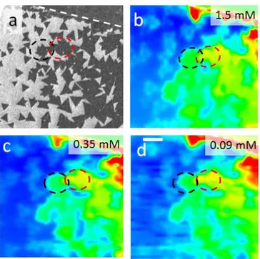
In order to investigate in detail the electric conductivity of this area, we have changed the redox mediator concentration used for SECM imaging. Very limited variation in the SECM response is observed upon concentration change even though the redox mediator concentration is increased by a factor of 50 between figure 4b and 4c. Figure 4d shows numerical simulation results also obtained for different redox mediator concentrations. The figure presents the SECM response as a function of the redox mediator concentration, for a flake having 50 µm edges. It shows that higher concentrations result in a lower feedback current. Indeed, an increase in the redox mediator concentration increases the solicitation of the sample to achieve a given feedback level, and it is more likely to lead to conduction limitations.[11] In fact, simulations show that an absence of feedback response change upon concentration increase -as observed in figure 4b and 4c- is the signature of resistance smaller than 103 kOhms (considering less than 10% current variation between 0.3 and 16 mM). This is in
accordance with literature regarding the conductive state of MoS2 transistors[21-22]. Then, a specific
numerical investigation was performed regarding the contact resistance between T6 and its neighbors.
We considered two highly conducting triangles connected at one of the vertex (see SI). Different contact resistances were considered. From the study –presented in SI-, we can conclude that despite the very tiny physical contact, the contact resistance is smaller than 100 kOhms. A more precise evaluation of the conductivities and contact resistances requires (i) a dependence of the SECM measurements with the redox mediator concentration and (ii) explicit consideration in the numerical simulations of all the flakes in the vicinity –not only those interconnected, similarly as for the investigation of GO flakes. [11]Notably, the low contact resistance between MoS2 flakes is not always
observed. Figure 5 shows SEM and SECM images of another area (same area as the one investigated in figure 2). On this figure, one can see that the area enclosed by the red dotted circle has a smaller response than the one in its vicinity, even at very low concentration (0.09mM). This comes from a limited electronic contact between the different MoS2 areas -despite a clear physical contact as
6
Figure 5. SEM and SECM images of CVD-grown MoS2 monolayer with different concentration of
DmFC. (b) [DmFC]=1.5 mM, (c) [DmFC]=0.35 mM, and (d) [DmFC]=0.09 mM. Other experimental conditions are similar to figure 1. Black dotted circles are centered on physically connected but electronically isolated flakes. The min-max color bar for each figure has been adjusted to highlight the contrast between the 2 areas observed with SECM.
From the area investigated in figure 3 and 4, we can conclude that there is a very large diversity of electrical connections between CVD-MoS2 flakes. Some flakes are very well electrically connected,
with low detectable contact resistance, while others are not connected at all –independently from the size of the physical contact between the conducting areas. Overall, the work shows how the complex electronic behavior of MoS2 flake assemblies (semiconducting nature, contact quality between flakes)
can be investigated with SECM. We showed that conventional experimental conditions (i.e. using Ferrocene as redox mediator) lead –in the best cases– to unstable measurements (cf. figure 2). On the contrary, using a redox mediator with a lower redox potential (decamethylferrocene for instance), we could obtain reliable SECM images of the flakes. The approach enables detailed electrical characterization without sample preparation (i.e. lithography), and is therefore an ideal tool to investigate systematically the diversity of configurations that is encountered. In the future, we plan to evaluate to what extent the different crystalline orientations of the crystals in contact are impacting the electrical communication between them. For instance, we can evaluate the contact resistance between MoS2 flakes when both triangles are pointing the same way, or when they are randomly oriented. It is
also possible to evaluate whether the contact resistance depends on the length of the contact region. Indeed, as shown in the present work, with the support of numerical simulation, it is possible to quantify the electrical conductivity/connectivity of the different areas.
Acknowledgement: “This work is supported by a public grant overseen by the French National Research Agency (ANR) as part of the “Investissements d’Avenir” program (Labex NanoSaclay, reference: ANR-10-LABX-0035)”
7
[1] Y. W. Zhu, S. Murali, W. W. Cai, X. S. Li, J. W. Suk, J. R. Potts and R. S. Ruoff, Adv. Mater. 2010, 22, 3906-3924.
[2] Z. He and W. Que, Applied Materials Today 2016, 3, 23-56.
[3] S. Najmaei, Z. Liu, W. Zhou, X. Zou, G. Shi, S. Lei, B. I. Yakobson, J.-C. Idrobo, P. M. Ajayan and J. Lou, Nat Mater 2013, 12, 754-759.
[4] S.-L. Li, K. Tsukagoshi, E. Orgiu and P. Samori, Chem. Soc. Rev. 2016, 45, 118-151. [5] H. Schmidt, F. Giustiniano and G. Eda, Chem. Soc. Rev. 2015, 44, 7715-7736.
[6] S. Amemiya, A. J. Bard, F. R. F. Fan, M. V. Mirkin and P. R. Unwin, Annu. Rev. Anal. Chem. 2008, 1, 95-131. [7] D. Polcari, P. Dauphin-Ducharme and J. Mauzeroll, Chem. Rev. 2016, 116, 13234-13278.
[8] R. Chen, N. Nioradze, P. Santhosh, Z. Li, S. P. Surwade, G. J. Shenoy, D. G. Parobek, M. A. Kim, H. Liu and S. Amemiya, Angew. Chem. Int. Ed. 2015, 54, 15134-15137.
[9] K. Jaouen, O. Henrotte, S. Campidelli, B. Jousselme, V. Derycke and R. Cornut, Applied Materials Today 2017, 8, 116-124.
[10] J. Azevedo, C. Bourdillon, V. Derycke, S. Campidelli, C. Lefrou and R. Cornut, Anal. Chem. 2013, 85, 1812-1818. [11] T. Bourgeteau, S. Le Vot, M. Bertucchi, V. Derycke, B. Jousselme, S. Campidelli and R. Cornut, J. Phys. Chem.
Lett. 2014, 5, 4162-4166.
[12] J. Azevedo, L. Fillaud, C. Bourdillon, J.-M. Noël, F. Kanoufi, B. Jousselme, V. Derycke, S. Campidelli and R. Cornut, J. Am. Chem. Soc. 2014, 136, 4833-4836.
[13] H. S. Ahn and A. J. Bard, J. Phys. Chem. Lett. 2016, 7, 2748-2752.
[14] H. Li, M. Du, M. J. Mleczko, A. L. Koh, Y. Nishi, E. Pop, A. J. Bard and X. Zheng, J. Am. Chem. Soc. 2016, 138, 5123-5129.
[15] P. R. Unwin and A. J. Bard, J. Phys. Chem. 1991, 95, 7814-7824.
[16] V. Ruiz, P. Liljeroth, B. M. Quinn and K. Kontturi, Nano Lett. 2003, 3, 1459-1462.
[17] P. G. Nicholson, V. Ruiz, J. V. Macpherson and P. R. Unwin, Phys. Chem. Chem. Phys. 2006, 8, 5096-5105. [18] A. Tarasov, S. Zhang, M.-Y. Tsai, P. M. Campbell, S. Graham, S. Barlow, S. R. Marder and E. M. Vogel, Adv.
Mater. 2015, 27, 1175-1181.
[19] C. M. Aguirre, P. L. Levesque, M. Paillet, F. Lapointe, B. C. St-Antoine, P. Desjardins and R. Martel, Adv. Mater.
2009, 21, 3087-3091.
[20] A. I. Oleinick, D. Battistel, S. Daniele, I. Svir and C. Amatore, Anal. Chem. 2011, 83, 4887-4893.
[21] C. J. L. de la Rosa, G. Arutchelvan, I. Radu, D. Lin, C. Huyghebaert, M. Heyns and S. De Gendt, ECS J. Solid State Sci. Technol. 2016, 5, Q3072-Q3081.