Analog Integrated Photonics
by
Cheryl M. Sorace-Agaskar
ARCHIVES
MASSACHUSETS INSTITUTEMAR 19 2015
LIBRARIES
Submitted to the Department of Electrical Engineering and Computer
Science
in partial fulfillment of the requirements for the degree of
Doctor of Philosophy
at the
MASSACHUSETTS INSTITUTE OF TECHNOLOGY
February 2015
@
Massachusetts Institute of Technology 2015. All rights reserved.
Signature redacted
A uthor
...
...
Department of Elec/rical ngineering [nd Computer Science
Signature redacted
January
3U,
2015
Certified by.
Signature
redacted
Michael R. Watts
Associate Professor
Thesis Supervisor
Certified by....
Accepted by ...
Franz X. Kaertner
Adjunct Professor
Thesis Supervisor
Signature redacted
. . . .. .. ...
d 0
Leslie Kolodziejski
Chairman, Department Committee on Graduate Theses
MITLibraries
77 Massachusetts Avenue
Cambridge, MA 02139 http://Iibraries.mit.edu/ask
DISCLAIMER NOTICE
Due to the condition of the original material, there are unavoidable
flaws in this reproduction. We have made every effort possible to
provide you with the best copy available.
Thank you.
The images contained in this document are of the
best quality available.
Analog Integrated Photonics
by
Cheryl M. Sorace-Agaskar
Submitted to the Department of Electrical Engineering and Computer Science on January 30, 2015, in partial fulfillment of the
requirements for the degree of Doctor of Philosophy
Abstract
Silicon photonics promises to revolutionize the field of optics by allowing for cheap, compact, low-power and low-noise optical systems on chip. In the past decade and a half, the basic functionality and acceptable performance of many individual in-tegrated photonic components have been demonstrated, particularly in the digital regime. However, there are several challenges remaining before these advances can truly be exploited to create large-scale, commercial, analog integrated photonic sys-tems. In this thesis, we address three of these challenges: (1) managing photonic lay-out and design of large-scale, complex systems jointly with CMOS driving circuitry, (2) integrating analog optical components in silicon, and (3) integrating photonic light sources in silicon.
First, we present a comprehensive VerilogA modeling toolkit for the simulation of large, joint photonic plus CMOS systems as part of the creation of a full photonic process design kit (PDK) and demonstrate its use. Other smaller contributions to the PDK and process are also described. Next, we describe the development of two modulators meant for analog applications: an integrated, linearized Mach-Zehnder modulator and an integrated single-sideband modulator, both of which are measured to have impressive performance. Then, we discuss the development of an integrated mode-locked laser to serve as an on-chip light source for precision, low-noise optical applications. Finally, we describe preliminary work toward creating fully integrated analog systems, with the ultimate aim of demonstrating a compact, low-noise mi-crowave oscillator.
Thesis Supervisor: Michael R. Watts Title: Associate Professor
Thesis Supervisor: Franz X. Kaertner Title: Adjunct Professor
Acknowledgments
As I finish my PhD, I am extremely grateful to the many wonderful people with whom I have worked over the years, and without whom this work would not have been possible. First and foremost I have to thank my wonderful advisors, Michael Watts and Franz Kdrtner, who provided me with the opportunity and funding to do the research presented in this thesis and whose insights were always helpful. Their support was invaluable. I would also like to thank Dr. Paul Juodawlkis for serving on my thesis committee, for his many helpful thoughts and questions and for being the driving force behind the IPI (now IQI) collaboration between campus and MIT Lincoln Laboratory from which I benefited significantly. I am privileged to have
had the chance to work with Prof. Vladimir Stojanovic whose dedication has been inspiring and whose comments have been invaluable. Prof. Leslie Kolodziejski has been a fantastic academic advisor; I couldn't ask for better. Prof. Terry Orlando was a great professor to TA for - I learned a lot from him. All of the professors I
took classes from over the years get my thanks for the knowledge they so wonderfully imparted.
I want to acknowledge Anatoly Khilo who took me under his wing when I started and explained the work with patience and care. Steve Spector was also instrumental in getting my photonics career off the ground. His dedication to getting things done, no matter what, was wonderful. Jonathan Leu did the CMOS driving circuitry for all the integrated devices and collaborated closely with me on the VerilogA code. His thoughtfulness, care, and attention to detail made working with him a joy. Patrick Callahan was also a joy to work with; I am glad that the mode-locked laser work is being left in such capable hands. I am grateful, too, for the work that the rest of the mode-locked laser team: Anna Baldcheva, Salih Magden, and Jonathan Bradley for the A1203 depositions and Katia Shtyrkova for measuring the full laser structures.
My officemate for the last three and half years, Ami Yaacobi, has been an
invalu-able source of sound advice, technical and otherwise, and I have benefited a lot from his insights. Dave Cole has also been a great source of wisdom on RF design and life
as well as great fun to work with. I give my appreciation to Michele Moresco, who worked tirelessly to make all of the mask runs happen, who was always extremely sup-portive of me and my work, and has been great to know. Speaking of fabrication runs, designs are nothing if one cannot test them, so I extend my thanks to the fabrication team at MIT Lincoln Laboratory, as well as at CNSE Albany for their fabrication efforts on this project. I would especially like to thank Douglas D. Coolbaugh, Gerald Leake, who always found a way to make things work.
Thanks always go to Dorothy, our wonderful administrative assistant in the OQE group, who truly makes the magic happen. And also to the many wonderful admin-istrative assistants we've had in the Photonics group during my time here: Laura von Bosau, Donna Gale, Gabrielle Brewington, Susan Davco and Stacy McGrath. (Thanks particularly to Laura for always having food available to satisfy my pregnancy-related need to eat constantly.)
There are others too numerable to name. All of my group mates, in both the Photonics and OQE groups, have been a wonderful source of support, whether it's bouncing ideas around, getting technical help in the lab, or advice on courses. I am blessed to have worked with so many wonderful, dedicated, talented people. My colleagues in the IPI/IQI initiative have also been fantastic and I am grateful to have worked with them and to be able to do so again in the future.
I couldn't have done it without the love and support of my friends and family. Kendra and Tom have been great sources of strength. My brother, Brian; parents; sister-in-law, Manishika; and mother-in-law have also all been amazing through all the ups and downs. And, of course, I am grateful to Ameya, the rock on which my world stands, and to Simon around whom it now turns.
God Bless, Cheryl Agaskar
Contents
1 Introduction 23
1.1 Silicon Photonics . . . . 23
1.2 Low Noise Microwave Oscillators . . . . 26
1.3 Integrated Photonic Low Noise Oscillator . . . . 28
2 Joint Modeling and a Process Design Kit (PDK) for a Photonics Platform 33 2.1 Introduction to the Silicon Photonics Process and Platform . . . . 35
2.2 A PDK for photonics - Layout and Verification . . . . 41
2.2.1 Layout . . . . 42
2.2.2 Verification . . . . 44
2.3 A PDK for photonics -VerilogA System Modeling . . . . 48
2.3.1 Why VerilogA? . . . . 51
2.3.2 Simulation Architecture and Philosophy . . . . 51
2.3.3 Mathematical Representation of Primitive Component Blocks 57 2.3.4 Simple Passive and Active Composite Devices . . . . 61
2.3.5 Full System Simulations . . . . 72
2.3.6 Advanced features . . . . 78
2.3.7 Summary and Future work . . . . 81
3 Developing Modulators for Analog Applications 83 3.1 Integrated Linear Mach-Zehnder Modulators . . . . 84
3.1.2 Approach and theory...
3.1.3 Design and DC results .
3.1.4 AC and Linearity results 3.1.5 Digital Performance...
3.1.6 Summary and Future work .
3.2 Integrated Single Sideband Modulator
3.2.1 Theory and Prior art...
3.2.2 Design, Layout, and Results
3.2.3 Summary and Future Work
4 Integrated Mode-locked Laser in the Silicon Photonics+CMOS plat-form 4 1 Tntroduction 4.1.1 Desired MLL 4.2 Platform Review an 4.3 Laser Components 4.3.1 Waveguide 4.3.2 Bends . . . 4.3.3 Loop Mirror 4.3.4 SA tapers . 4.3.5 Output taper 4.3.6 Erbium Tren Components 4.4 MLL Architectures a 4.4.1 Passive Desig 4.4.2 Active Desigi feaure... features . . . . I Basic Structures . .
. . . .
.
. .
...
s .. . . . ch Transitions, Active nd Lasing Results . . ns . . . .4.5 Summary and Future Work
122 123 124 126 132 136 138 141 Laser Devices and Other
. . . . 142
. . . . 147 . . . . 14 7
. . . . 154 . . . . 158
5 Integrated Pound-Drever-Hall Loops and Other Integrated Systems 161 5.1 Other Devices and Integration with CMOS circuitry . . . . 161
5.2 Fully integrated PDH Loop . . . . 165 88 95 100 101 103 103 104 114 119 21 121
..
5.3 Balanced Detector and Frequency Divider . . . . 172
5.4 Summary and Future Work . . . . 173 6 Summary of Contributions and Parting Thoughts 175 A Overview of Modulator Approach and Design Process 177
List of Figures
1-1 Silicon photonics provides a way forward for drastically reducing the size, weight, and power of large optical systems, including phased array antennas (top) and LIDAR systems (bottom). Figures from [5, 116, 7,
8], figure based off figure by Ami Yaacobi. . . . . 24
1-2 A worker on a CMOS silicon fabrication line. Image from [135]. . . . 25
1-3 Silicon photonic systems on a chip. Clockwise from top left: 4-channel on chip WDM link [126], on-chip phased-array [5], integrated hetero-dyne interferometer [115], on-chip optical trapping for biomolecule ma-nipulation [129], integrated photonic front-end for an analog-to-digital converter [1], on-chip LIDAR steerable antenna [116]. . . . . 27
1-4 (a.) Poseidon Scientific (now Raytheon) sapphire loaded cavity os-cillators. Rack mounted sapphire loaded cavity oscillator (top) and
Shoebox Oscillator @(bottom), From [123] (b.) Schematic of NIST
frequency divider oscillator. From [1181. . . . . 29
1-5 Proposed integrated low-noise microwave oscillator . . . . 30
2-1 (a) Photonic-only chip layer stack. All layers other than the Er Doped
A1203 (light pink) are fabricated at CNSE Albany. The A1203 is
de-posited at MIT. (b) The full 3D integrated layer stack showing pho-tonics wafer flipped and wafer bonded to the CMOS wafer (From
1471).
The only difference among the photonics layers compared to (a) is that the laser trench now comes in from the back (silicon handle side) instead of the the front (metal side) to allow for post-3D-integration deposition of the A1203 at MIT. As before, the rest of the fabrication
is carried out at CNSE Albany. . . . . 36
2-2 Example final doping distribution showing density of p-type (blue) and n-type (orange,red) dopants in a MZ diode modulator (top), a disk diode modulator (middle) and an integrated heater (bottom) . . . . . 39
2-3 Full Silicon MZM with CMOS driving circuitry is laid out in cadence.
Simple shapes (such as basic waveguides and tapers) are combined to create more complicated structures (such as the ridge taper shown), these more complicated structures (ridge taper, coupler, phase shifter, heater) are combined to create the full photonic layout. The full cir-cuit layout is added to the photonic layout. Thus, the photonic and electronic pcells together create the layout of the full system. Designs therefore have the ability to include all 100+ photonic and CMOS lay-ers, allowing the full system to be viewed together. A zoom in of the heater and heater driver section of the full layout is shown at bottom. 45
2-4 (a) Schematic of labeling for connectivity for LVS verification (b) Ex-ample photonic layout including labels . . . . 47
2-5 A ring resonator (diagrammed at top) is broken into components. The
VerilogA modules for these components are placed and connected in a schematic in Cadence (middle). A schematic symbol is created to represent this schematic block (bottom). This symbol can be inserted wherever a ring is needed as opposed to having to redraw the mid-dle block. Relevant variables are passed through this symbol to the underlying schematic. . . . . 56
2-6 (a) Diagram showing the components of a ring resonant filter and ac-companying layout using our toolkit in Cadence Virtuoso. (b). A full link schematic including laser and photodetector is created to simulate the performance of the device. (c). Amplitude and phase response of the ring showing good agreement between VerilogA simulations and MATLAB transfer function code. . . . . 62
2-7 (a). Diagram showing the components of a ring resonant filter with drop port and accompanying layout using our toolkit in Cadence Vir-tuoso. (b). Amplitude response of the ring showing output intensity in the through and drop port. One can see that the critical coupling has better extinction in the through port but less power in the drop port output, while matched coupling has worse extinction and higher drop port output power, as expected. Good agreement is seen between VerilogA simulations and MATLAB transfer function code . . . . 65
2-8 (a). Diagram showing the components of a two ring series filter with drop port and accompanying layout using our toolkit in Cadence Vir-tuoso. (b). Amplitude response of the ring showing output intensity in the through and drop port showing good agreement between VerilogA simulations and MATLAB transfer function code. . . . . 66
2-9 (a) . Diagram showing the components of a single ring modulator and accompanying layout using our toolkit in Cadence Virtuoso. (b). Modulator amplitude transfer function as a function of applied phase-shifter bias, showing good agreement between VerilogA simulations and MATLAB transfer function code. (c). Schematic of full like. Output from a CW laser is feed into a ring modulator driven by a PRBS source. The output of the modulator is sent to a photodiode. . . . . 68
2-10 Simulation output, showing electrical driving voltage, field amplitude inside the ring, through port field amplitude, and output of photodiode. 69
2-11 (a.) Diagram of single side band modulator component system (from reference [1291) and accompanying layout using our toolkit in Cadence Virtuoso using basic components (couplers, heaters, phase-shifters).
(b) Fouier transform of SSB output as a function of modulation
am-plitude. Input CW signal is shown in black in upper left. Following graphs show steadily increasing modulation depth. Increase in power transferred to desired sideband and accompanying increase in power in undesired harmonics is seem. VerilogA and MATLAB code show good agreem ent. . . . . 70
2-12 (a). Schematic of WDM link with four PRBS channels and one clock channel. (b) real part of signal on WDM waveguide (top), input and output of modulator channels (bottom four channels). . . . . 74
2-13 Schematic of PDH loop (after citen19) and schematic layout in Cadence
Virtuoso. (b) PDH error function in low and high frequency regime, showing good agreement between MATLAB and VerilogA code. (c). Phase noise simulation done using our toolkit showing noise of the free-running CW laser (red) and of laser locked to cavity (black) showing successful phase-noise suppression. . . . . 76
2-14 (a) Schematic layout of PDH loop using nonideal photonics and full driving circuitry in Cadence Virtuoso. (b) Left: Output PDH error function in low frequency regime. Distortions are clearly visible, but sign is still correct allowing loop to lock. Right: Laser frequency locks to cavity reference in 100nm (red), real part of laser electric field as locking occurs (green). . . . . 77 2-15 A Gaussian pulse undergoes dispersion in a waveguide. . . . . 81
3-1 Schematic of MZM Layout. From [981. . . . . 89
3-2 (a) Cross-section of phase-shifter showing doping distribution, (b) Sim-ulated effective index and effective field loss of phase-shifter as a
func-tion of applied bias. From [941. . . . . 97
3-3 Simulation output showing predicted distance of the third harmonic below the fundamental as a function of input drive power. Predicted
input IP3 was 64dBm. From [94]. . . . . 98
3-4 Schematic of Measurement Setup. From [94]. . . . . 98 3-5 (a) Output of MZM as a function of heater bias, showing the full range
of the output can be achieved. Heater is 100pm in length, length of phase-shifter section (unbiased) varied from 500-2000pm (b) Output of the MZM as a function of DC phase-shifter bias, showing full device operating range can be achieved, (c) Extracted phase as a function of bias for devices of different length. Results match well to original theory. Measured VwL = 0.27Vcm. (d) Graph of reverse-bias current showing breakdown around 7V. From [94]. . . . . 99 3-6 High speed performance of MZM, showing 3dB roll-off of 25GHz in
3-7 Comparison of measured and simulation output of predicted distance
of the third harmonic below the fundamental as a function of input drive power. Good agreement is seen between simulation and theory. Predicted input IP3 was 64dBm. Measured input IP3 was 68.4dBm.
From [941. . . . . 101
3-8 SFDR measurement of the device. Showing (a) the SFDR intercept
with the noise floor at -127dBm in our measurement setup. The SFDR was measured to be 82.ldBHz2/3. (b) The fundamental at -44.9dBm and the third harmonic in the noise floor. From [94] . . . . 102
3-9 Open eye diagrams at 1 Gb/s, 5 Gb/s, and 12.5 Gb/s. . . . . 102 3-10 (a) Schematic of Single Sideband Modulator (b) Equivalent Layout
with all heaters in inner arms, (c) Frequency domain representation of the signal at each point along the modulation path. . . . . 106
3-11 Labeled diagram of SSB modulator . . . 107
3-12 As RF drive voltage increases power transfer to desired sideband
in-creases, but undesired harmonic terms increase faster, making choice of operating voltage a trade off in loss vs. nonlinearity. . . . .111
3-13 (a.) Effects of variation in RF signal phase on SSB output. (b.) Effect
of incorrect bias on one heater inside one of the nexted MZMs. Note the appearance of the even-ordered harmonics and the carrier. . . . . 115
3-14 Measurement set-up. * = laser, OSA = optical spectrum analyzer, SG = signal generator, DC = DC power source. From [?] .. . . . . 116 3-15 Output of single sideband modulator, showing carrier suppression greater
than 18dB and suppression of other sideband and tones more than
15dB. The expected power loss is -9.3dB and the measured loss is -10.4dB. From [?]. . . . . 117
3-16 Shift in lower sideband location as a function of modulation frequency. From [?]. . . . . 118
3-17 Single-sideband operation in same device at 1570nm and 1590nm.
Car-rier and other sideband suppression >15dB can be seen at 1570nm, and carrier suppression >10dB and other sideband suppression >25dB can be seen at 1590nm. From [?]. . . . . 118
4-1 (a) Full Photonic + CMOS layer stack after [47] and chapter 2, (b) Short-loop layer stack, which includes only the nitride and Er:A1203
layers. . . . . 123
4-2 (a) Diagram of passive spiral laser architecture with main component parts labeled, (b) Diagram of passive compact s-bend laser with main component parts labeled. . . . . 125
4-3 (a) cross section of gain waveguide where orange = nitride, blue = ox-ide, and green = Er:A1203. Marbled region at edges denotes roughness
(see below), (b) Fundamental TE mode in waveguide for laser center and pump wavelengths, (c) Overlap of the laser mode with the pump are of the gain medium. . . . . 127
4-4 (a) Loss vs. roughness width (width of the center region is equal to 50 microns minus two times the roughness width). Grey region represents expected waveguide gain. As can be seen loss in the Fundamental TE mode remains low while loss in the other modes is high, (b) Top view of trench width in roughened waveguide along with cross sections at two locations in the roughness. . . . . 129
4-5 Experimental transmission results for roughened waveguides: multi-mode beating is clearly seen for the case of no roughness (blue line), a roughness width of 5 or 7 microns (red and green lines) removes un-wanted modes (as seen by lack of beating), but does not add to loss, while a roughness width of 10 microns (black line) causes extra loss. . 130
4-7 Total dispersion for the best (left) and worst (right) A1203 material dispersion. Anomalous (negative) dispersion is achieved in the best case for thick layer heights. For thinner layers or the worst case A1203 material dispersion total dispersion is normal but, in most cases, small. 132 4-8 Simulated bending loss vs. radius (in mm) for gain waveguide bend.
Inset figures show modes at different film heights relative to bending radii (center of bend is on right). From left to right: 1pim film height and 3mm bending radius: mode is well confined to center of the guide, 1.6[tm and 9.3mm radius: one can see that the mode is starting to slide toward the edge of the trench, 2.0pm film height and 15mm radius: mode is no longer confined by nitride guide, but rather by side of the
A1203 trench. . . . . 134
4-9 Simulated bending loss vs. radius for nitride waveguide bend . . . . . 135
4-10 Diagram of bend, where dark green is nitride waveguide and olive green is the trench. bend parameters 1-3 are described in the table below. . 136
4-11 (a). Diagram of loop mirror as drawn on the mask. (b) Comparison of coupled mode theory vs. FDTD simulations. . . . . 137
4-12 (a) Measured loop mirror reflection is in good agreement with the-oretical predictions. (b) Simulated reflection for various wavelengths. Reflection percentages are similar across the 1530-1570nm Erbium gain band. Reflection at the 1480nm is lower, as desired, but could be fur-ther optim ized. . . . . 139
4-13 (a) Taper type one where both nitride layers are tapered together. (b) Taper type two where each nitride layer is tapered separately. . . . . 140 4-14 Loss in dB vs. wavelength for round-trip coupling to SA. From [471 . 140 4-15 Raw data of best performing taper coupled to 3p/m fiber for each taper
4-16 Measured and predicted loss vs. taper width for taper type one. As can be seen an extra 1-1.5dB of loss is seen in the measured results, though the trend agrees. Additionally, length has an effect in the measured results, with the longer device performing worse. . . . . 143 4-17 Diagram of Er trench transition structure (top) and FimmwaveTM
modesolver (left) and transmission simulation of same (right) . . . . . 145 4-18 (a) Diagram of passive spiral laser architecture, (b) photograph of
spi-ral lasers on chip. . . . . 148 4-19 Green florescence from high power 1480nm pump outlines the laser
structure. ... ... 149 4-20 (a) Ouput spectrum of cw laser as a function of pump power. (b) Laser
output power vs. input power on chip. oscillation threshold is around 1.6W. This laser had a mirror reflectivity measured to be 30%. From
[47]. . . . . 150
4-21 (a) RF spectrum of laser in Q-switched mode-locking regime, (b) Oscil-loscope trace of same, (c) Zoomed in oscilOscil-loscope trace of pulse burst.
From [471. . . . . 151
4-22 (a) Diagram of compact passive s-bend laser architecture. . . . . 152
4-23 Schematic of compact s-bend laser to be pumped at (a) 980nm and (b)
1480 n m . . . . . 153
4-24 Measured transmission through passive s-bend laser architecture as a function of wavelength. . . . . 154 4-25 Fluorescence in compact s-end laser designed for 980nm pumping. A 3
way pump splitter (out of the frame) couples the pump light into each of the three gain sections. . . . . 155
4-26 Diagram of actively mode-locked s-bend laser configuration including MZ modulator for active pulse shaping and intracavity controls for comb stabilization. Phase-shifters are shown in gray, the intracavity heater in brown, the silicon in gold, and the nitride in red. . . . . 157
5-1 (a.) Mask layout of integrated heater, (b.) Phase change through heater vs. input DC power . . . . 162 5-2 Integrated Germanium Photodetector (a.) Layout of two different
de-vice variations, (b) Schematic of TIA drving circuit for PD, (c.) Output current vs, optical power out of fiber input to chip for 8x1pm (red) and 8x3pm (green) 3D integrated PDs with 5kQ TIA resistance tested at 1530nm, (d.) Speed measurements of 8x1pm (blue) and 8x3pm (red)
3D integrated photodiodes with 5kQ TIA resistance. . . . . 164
5-3 Plot of single sideband phase noise due to thermal fluctuations for ring variations on mask. . . . . 166
5-4 Diagram of PDH Loop. Blue denotes electrical components, and pink photonic ones. . . . . 168 5-5 PDH error signal in the low frequency (left) and high frequency (right)
operating regions. Figure from [69]. . . . . 170 5-6 Simulation output of Pound-Drever-Hall Loop in the low frequency
regime. Results previously shown in Figure 2-14. . . . . 172 5-7 Cadence layout of PDH photonics-only loop (top, variation with nitride
rings used as high-Q reference cavity and integrated ring lasers), and photonics+CMOS loop (bottom, same variation). . . . . 173 5-8 (a.) Zoom in of Cadence layout of balanced detectors. Detectors shown
are photonics only. Edge of pads for CMOS integrated balanced detec-tors which are interwoven are visible at right. (b.) Layout of CMOS integrated frequency divider loop consisting of SSB modulator and bal-anced detector. . . . . 174
A-1 Diagram of simulation flow for modeling silicon reversed biased diode
plasma dispersion effect phase shifters. Figure previously appeared in
List of Tables
4.1 Summary of measurements of compact Er:A1203 bend structures. 136
4.2 Summary of measurements of taper structures. . . . . 144 4.3 Summary component loss measurements. . . . . 155
Chapter 1
Introduction
1.1
Silicon Photonics
Silicon photonics is the field in which silicon integrated-circuit technology is used to transmit, manipulate, and process optical signals. It promises to bring the advantages of semiconductor process technology to the optical systems that have created the backbone of the telecommunications industry and that promise improved performance on a variety of electric systems from analog-to-digital converters (ADCs) to arbitrary-waveform generators (AWGs) [1, 2, 3, 4]. Now, in particular, is a time of great promise in the field of silicon photonics, as many of the basic devices needed for these systems have been demonstrated and optimized to the point where they have acceptable performance metrics.
There are a number of advantages to integrated photonics in general and inte-grated silicon photonics in particular. First, it leverages the huge advances made in semiconductor processing technologies over the last half century and brings them to the optical regime, thus, enabling small precision devices to be fabricated cheaply and in large number. Thus, silicon photonics promises to unite the discrete components currently used to create optical communication and other table-top systems onto a single chip and allow for affordable mass-production of these chips for use in prod-ucts. Movement of optical systems on chip significantly reduces the size, weight, and power requirements of these systems, further widening the situations in which an
ap-Figure 1-1: Silicon photonics provides a way forward for drastically reducing the size, weight, and power of large optical systems, including phased array antennas (top)
and LIDAR systems (bottom). Figures from [5, 116, 7, 81, figure based off figure by
Ami Yaacobi.
plications for which they can be used [4]. For example, silicon photonics is currently working to replace large microwave phased array beam steering and LIDAR appli-cations, where giant antenna arrays and large systems are currently in use at long wavelengths, with small on-chip systems that work at shorter optical wavelengths as
illustrated in Fig.1-1 [5, 1161.
This miniaturization is made possible not just by the fact that small features can be fabricated, but also by the fact that optical devices of such small size can work.
A key reason for this is the high index contrast between silicon and SiO2, silicon's
native oxide. This high index contrast means that optical mode areas can be kept small and guided through tight bends. It reduces optical power requirements, and can even facilitate nonlinear interactions, should they be desired [116]. While the high index contrast can lead to fabrication sensitivities, much recent work has been done to overcome this either through the creation of robust devices or improvement in fab-rication techniques (see, for example, [9]). Moreover, the use of silicon allows for the
Figure 1-2: A worker on a CMOS silicon fabrication line. Image from [135].
creation of active devices, such as diodes, used for the creation of modulators (which
transfer electrical signals onto an optical carrier), and the silicon process is
materi-ally compatible with the inclusion of germanium layers for optical detection (which
turns optical signals into electrical ones). Importantly, Silicon is transparent in both
telecommunications bands (1.3pm and 1.55pm) as well as at longer IR wavelengths,
and its process is also materially compatible with the inclusion of nitride layers which
are transparent in the visible as well as the IR, and are useful for nonlinear as well
as quantum applications [10, 11]. Further, though its indirect bandgap prevents it
from being used to create a light source, various laser sources have been successfully
bonded onto or grown on silicon photonic chips [12, 13, 14]. Finally, the use of a
silicon platform, the same material system used for the CMOS electronics industry,
for photonics allows for easy integration with complicated electrical driving circuitry
through either monolithic integration [15] or wafer bonding [126].
In the last decade and a half, much work has been done on individual silicon
photonic devices, including modulators [9, 93], photodetectors [19], waveguides [125],
ring filters [21, 221, bonded lasers [23, 14], erbium doped lasers [24], vertical couplers and antennas [5], among many others. This has allowed more recent work to focus on using these devices to create systems, and to apply the technology to create state-of-the-art or near state-of-state-of-the-art integrated photonic versions of both existing systems and novel optical systems capable of surpassing existing system performance, such as WDM communication links [126], phased arrays [5], LIDARs [116], heterodyne interferometers 1115], photonically-assisted ADCs [1, 128], AWGs [?, 3], sensing and optofluidics [129], and advanced signal processing applications [131], among many others. However, more work needs to be done to truly leverage silicon photonics' advantages in the systems world, as a complete silicon photonics platform needs to be established. This will be discussed more in Chapter 2.
1.2
Low Noise Microwave Oscillators
One application of particular interest is that of low noise microwave oscillators. There are many applications, from radar to coherent communications to global positioning systems, to precision noise measurement systems where low noise microwave oscilla-tors are important [117, 118, 119]. Very low noise oscillaoscilla-tors lower the noise floor in coherent detection and communication systems so that extremely weak signals can be detected, such as the Doppler shift from a person walking in the observation region of a Doppler radar system [119]. Oscillator noise performance is often characterized
by giving the single-sideband phase noise at a given frequency offset from the
car-rier frequency -typically a 1 Hz offset is used in very low noise systems. For very low noise systems, the given frequency offset is usually a 1Hz offset. The single-sideband phase noise is equal to half the power spectral density of the phase error
(C(f) = fco (A(t)A#(t + T))ei2xf/rdT where
f
is the frequency offset form the carrier and L(f) is the single-sideband phase noise [119]).While very low noise oscillators have been demonstrated, these oscillators are often large and require cryogenic cooling or extensive temperature or cavity stabilizing circuitry [117, 122, 121]. They are also very expensive. The current state of the art is
Figure 1-3: Silicon photonic systems on a chip. Clockwise from top left: 4-channel on chip WDM link [126], on-chip phased-array [5], integrated heterodyne interferometer
[115], on-chip optical trapping for biomolecule manipulation [129], integrated photonic
front-end for an analog-to-digital converter [1], on-chip LIDAR steerable antenna
the Poseidon sapphire loaded cavity oscillator pictured in Fig.1-4.a., which achieves a phase noise of less than -100dBc/Hz at a 100Hz offset in a "compact" rack device or
shoebox sized device [123, 124, 1301. This latter weights 14.5 pounds [130]. While this
is a significant advancement over other systems, it is still too large to be included in, say, a hand-held radio or small system designed for field use. Additionally, it is desired to make an oscillator even less sensitive to environmental noise factors, especially vibrations, to truly allow for practical use. Cost is another consideration as a cheap, mass-producible component can be used in a much wider variety of systems. However, using sapphire cavity technology, it is not clear how oscillator size, sensitivity, and cost can be significantly more reduced.
Recent developments out of NIST on frequency dividers provide a possible path forward. In [118], a cavity stabilized continuous wave laser was used to stabilize a comb line of a mode-locked laser (MLL). Together with a lock on the mode-lock laser's carrier-envelop-offset frequency, this allowed for a highly stabilized MLL comb, which, when beat on a photodetector created a very low noise microwave signal (see Fig.1-4.b.). A single sideband phase noise of less than -100dBc/Hz at a 1Hz offset was achieved in this system at a microwave carrier frequency of 10 GHz - .which is the lowest phase noise that has been achieved to date at this carrier frequency [1181. At first, because this is a large, table top system, it may not seem to help in the quest for a small, robust, cheap, portable low noise microwave oscillator. However, because this system is based on optical components, system size, weight, and power requirements can be drastically reduced through on-chip integration - that is through movement to a silicon photonic platform.
1.3
Integrated Photonic Low Noise Oscillator
A proposed erbium silicon photonic integrated oscillator for generation of an
ultra-low noise microwave signal, inspired by the NIST system, is shown in Fig.1-5 and is under development in our group [119, 120]. As the details of this system have been presented elsewhere [119] only a quick outline will be given here. The goal of this
3D m
OFZCI
515T~ iim IGHz
(a) (b)
Figure 1-4: (a.) Poseidon Scientific (now Raytheon) sapphire loaded cavity
oscilla-tors. Rack mounted sapphire loaded cavity oscillator (top) and Shoebox Oscillator
@(bottom),
From [1231 (b.) Schematic of NIST frequency divider oscillator. From
[118].
system is to reach a single-sideband phase noise of -115dBc/Hz at a 1Hz frequency
offset.
A schematic diagram of this oscillator is shown in Fig. 1-6. The basis of the system
is a continuous wave (CW) laser locked to a reference cavity, here a high-Q, passive,
athermal ring resonator, through a Pound-Drever-Hall locking loop (bottom left box
of Fig.1-6). This loop will be discussed further in Chapter 5. The output of the
stabilized CW laser is split onto three different waveguide paths.
One of these outputs is used to transfer the lower frequency noise of the locked
CW laser to a mode-locked laser (MLL) comb (upper left block in Fig.1-6). In this
loop, a single line is filtered out of the output of the mode-locked laser, combined
with the CW laser tap in an adiabatic 3dB coupler, and beat on a photodetector.
More precisely, the two outputs of the coupler each feed one photodiode in a balanced
detector. The frequency difference of the two lasers is reflected in the frequency of
the signal output from the balanced detector. The use of a balanced detector not
only increases the signal-to-noise ratio (SNR) by 3dB, but also serves to cancel the
common-mode noise. The output is then fed back on the MLL in such a way as
to adjust the repetition rate of the laser and lock the comb line to the CW laser
1Wj
Figure 1-5: Proposed integrated low-noise microwave oscillator
frequency, while preventing any change in the carrier-envelope-offset frequency. This loop, thus, locks the MLL comb in place. Because of the extremely low timing jitter and noise in the MLL, the output pulse train is very stable, and would create a very-low noise microwave signal if incident on an appropriate photodetector. However, due to the on-chip nature of our components, it is difficult to get enough power out of the MLL to create a strong microwave signal; we therefore add an extra loop (right box in Fig.1-6). This is where our system deviates from the NIST demonstration.
Up to this point the system has basically mirrored the NIST system in integrated
form, however, whereas, in the NIST frequency divider the output of the MLL is sent directly to a photodetector, here we have this extra step.
In this last loop, a second line is filtered out of the MLL comb, separated from the first by the desired microwave frequency. This line is then beat against one of the remaining CW outputs on a second balanced detector. However, in this case a single-sideband modulator (SSB) is used to frequency shift this CW laser output and lock it to the second filtered MLL line. The output signal from the balanced detector is fed back on to a voltage controlled oscillator (VCO) that serves as the
SSB driver and controls this frequency shift. The frequency shifter CW laser line
is then combined with the last, unmodified CW laser line and the two are beaten together on a final detector to create the desired microwave signal. This last loop serves to transfer the low noise of the MLL comb to the split CW laser output, while allowing the oscillator to take advantage of the larger power (and therefore lower shot noise) in the CW laser output. The ultimate goal is an RF microwave oscillator at 20GHz with a single-sideband phase noise less than -115dBc/Hz at a 1Hz offset, an RF oscillator output power of 100mW, a power consumption of less than 15W, and a substrate area requirement of less than 1cm2
.
The work described in this thesis aims to support the development of the above oscillator from beginning to end: starting with the development of the integrated plat-form, layout, and systems codes necessary to fabricate the oscillator system, through the development of oscillator devices, and ending with some preliminary work on the control loop building blocks of system, in particular the Pound-Drever-Hall locking
loop. The layout of this thesis is as follows. In Chapter 2 we discuss the silicon photonics platform under development in our group. We summarize the photonics process and present work done to facilitate the creation of an integrated photonics
+ CMOS electronic process design kit. A key piece of this work is the development
of a VerilogA modeling toolkit to facilitate joint photonic+CMOS modeling of large, complex systems, such as our oscillator loop. Chapters 3 and 4 discuss the creation of necessary devices in this platform. Chapter 3 focuses on the silicon layer and discusses the creation of modulators. A linear Mach-Zehnder modulator (MZM) is discussed first, and then two such MZMs are nested to form the single-sideband mod-ulator needed in the oscillator. Chapter 4 discusses the creation of the integrated mode-locked laser. Chapter 5 builds on these devices and presents preliminary work on the sub-loops in the overall oscillator loop. Finally Chapter 6 provides a summary of the contributions of this work and a discussion of directions for future work.
Chapter 2
Joint Modeling and a Process Design
Kit (PDK) for a Photonics Platform
Integrated photonics stands at a tipping point similar to that of the electronics indus-try a half century ago. In the past fifteen years most work has focused on the devel-opment of individual devices, aiming to demonstrate basic functionality and achieve performance metrics necessary for use in larger systems. During this time impressive results have been achieved for many individual devices including modulators [25, 9J, photodetectors [19], ring filters [21, 22], integrated lasers [12, 13, 14], couplers [26, 271, on chip tapers [281, and many other components. Because they are integrated, many of these components promise equivalent or better performance than existing table-top components, while being smaller, lighter, and more power efficient. They are often less sensitive to environmental variations, such as vibrations, and have other specific use-case related advantages (such as higher confinement leading to smaller mode area and tighter power confinement yielding increased nonlinear effects) [29J.
The state of the art in optical components is now advanced enough that the focus has shifted to leveraging them for use in optical systems. Stand alone integrated components have been included to improve the performance of table top systems (see, for example [301), but the ultimate goal is fully integrated systems that both have state of the art performance and are cheaply mass producible (for example [1]). While many integrated systems have been demonstrated [5, 31, 129, 126], these systems have
either been limited to no more than a couple dozen components [1, 31, 129, 1261 or, have had a simple architecture, which kept performance easily predictable and allowed for easy layout, despite having many components [5]. Design has usually been done in a pieced together manner with component simulations done separately and pieced together and together with the outputs of electrical driving circuity (when there has been any electrical driving circuity) roughly at the end. In order to be able to design and layout truly complex systems, especially ones that include electrical drivers, a design platform is needed. This chapter will discuss such a platform.
Because the development of the photonics industry really parallels that of the electronics industry and because many silicon photonics devices are even fabricated in the same foundries and clean rooms that make electronic devices (as is the case in this work among many others), it makes sense to look to the electronics industry to see how to design such a platform. One key idea that we can take from that industry is the idea of a multi-project run (aka a multi-project wafer service). This is where a foundry combines designs from many different organizations (small companies, stu-dents, universities, etc...) and fabricates them all on the same wafers using the same mask sets. Because foundry services are extremely expensive, putting many projects on the same run allows for the costs to be spread out between groups and greatly reduces the barrier to entry. In order to make the foundry services accessible to these groups, foundry companies create and distribute process design kits (PDKs). PDKs aim to give designers all the information that they need in order to design into the foundry process including fabrication information (available material layers, design rules that need to be followed) and standard device libraries. They will be discussed in more detail in the sections below, as we discuss the creation of the photonics version
of such a PDK.
There have been some forays into providing silicon photonic multi-project runs, including [32], which has since ceased operation, [341, which does not offer light source integration or a complete design kit (no co-simulation with CMOS is available) and
[33], which is a custom design studio which does in house fabrication. A slightly
infancy. In our group we have found the need to develop equivalent services for use in house and we coordinate internally across many projects, designers, and groups. Our group's wafers are in some ways their own mini one organization multi-project runs.
2.1
Introduction to the Silicon Photonics Process
and Platform
In order to set up a multi-project run for photonics, it is necessary to create a photon-ics platform. A true platform consists of a fabrication process through which devices and systems can be physically realized as well as a process design kit (PDK), usu-ally including a device library, that allows designers to truly utilize the fabrication process. That is, the PDK contains all the relevant and necessary information for designers to create and submit designs to the fabrication facility for production.
The first part of the platform, therefore is the fabrication process. The devices discussed in this thesis were fabricated at the 300mm CMOS foundry at the College of Nanoscale Science and Engineering (CNSE) at the University of Albany in Albany New York using a process they developed in collaboration with our group, and Pro-fessor Vladimir Stojanovic's group at Berkeley. Some early work on this process was also done in collaboration with MIT Lincoln Laboratory. The process will be outlined here. It consists of a photonics wafer 3D bonded to a CMOS wafer via through oxide vias (TOVs). The CMOS wafer is made using a standard CMOS process on a 65nm node and contains electronic driving and other desired circuitry. The photonics wafer, which contains the photonic part of the designs, is fabricated using the developed, custom process for silicon photonics. It consists of both active and passive photonic devices as well as a trench in which erbium doped A1203 is deposited to act as a gain medium for on chip lasers. Both photonics-only (without CMOS) and 3D-integrated (with CMOS) wafers can be returned from the fabrication facility as desired.
photonics-(a) (b)
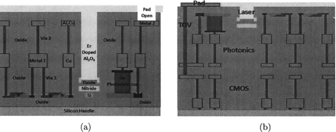
Figure 2-1: (a) Photonic-only chip layer stack. All layers other than the Er Doped
A1203 (light pink) are fabricated at CNSE Albany. The A1203 is deposited at MIT.
(b) The full 3D integrated layer stack showing photonics wafer flipped and wafer
bonded to the CMOS wafer (From [47]). The only difference among the photonics layers compared to (a) is that the laser trench now comes in from the back (silicon handle side) instead of the the front (metal side) to allow for post-3D-integration deposition of the A1203 at MIT. As before, the rest of the fabrication is carried out
at CNSE Albany.
only and 3D-integrated cases. As shown, the platform centers around a silicon layer patterned to provide waveguides for routing the light. The high refractive index of silicon allows for tight bends, high confinement, and thus, small devices, while the infrastructure developed over many years for the electronics industry and the fact that silicon is transparent at telecom wavelengths allows for low loss. (The former drives down losses from roughness, etching, and patterning, and the later yields low material loss). The silicon layer has both a full height and a half-height, ridge etched section. The ridge etch serves several purposes, among other things: it allows for the creation of rib waveguides, which in turn allow for easy contacting to active devices
[36]; it can be used to create polarization rotating devices which convert between the TE and TM modes of a waveguide [37; it can be used for symmetry breaking in
vertical couplers to allow for more than 50% upward coupling [?].
The silicon layer is also used to support active devices. The fabrication process contains four doping masks; one each for a high and a low doping of acceptors and donors (n+, p+, n, and p). There are also two doping impants to support the photodetectors. The low dopants (n and p) are used where the doping overlaps with
the optical mode, allowing the creation of an active device while keeping optical losses low. In early work, low doping concentrations were quite low (on the order of 1017,
or sometimes even high 1016) [38]. However, because higher doping levels allow for
faster and smaller diode devices with minimal loss or heater performance penalties, doping levels used in the literature have been continuously increasing 19] and those picked for use in this process were chosen to be higher - on the order of 1 - 5 x 10¹⁸.
The high dopants (n+ and p+) included in the process contribute a prohibitively high optical loss and are used away from the optical mode to allow for lower resistance, high speed contacts.
While they can be used however desired, the doping impants in our process are generally used to create two types of active devices: diodes and resistors. The resistors serve as heaters, shifting significantly, but at low speed, the index of refraction of the waveguide through the thermo-optic effect, and thereby creating a phase shifter. In the thermo-optic effect, the index of the waveguide is changed according to An = no
+
(dn/dt)AT where dn/dt ~ 2 x 10⁻⁴/C
in silicon, and where the loss change is minimal [39]. Such resistive heaters are useful in setting the bias points of Mach-Zehnder modulators [36] and ring modulators and filters [22, 40], and for controlling phases in antenna elements of phased arrays where their small size is essential [5].Diodes structures aim to take advantage of the faster, but comparatively weaker, plasma dispersion effect (PDE). Here, a change of carrier concentration creates a change in loss and refractive index of a material through its effect on the material band structure. The PDE can be theoretically modeled through the Drude equations [411, and has also been experimentally measured by Soref et al [42]. In the literature an empirical fit to Soref's data for index of refraction, n, and loss coefficient, a, given
by:
An = -8.8e - 22AN - 8.5e - 18AN. 8
Aa = 8.5e - 18AN + 6e - 18ANh (2.1) is often used. However, this equation does not fit the data precisely and does not
account for wavelength. Because of this often other fits to the same data set are used when more precision is desired [93].
A p-n diode is the simplest, non-metal, device useful for changing carrier
con-centrations in a waveguide. It can be operated in one of two regimes: forward or reversed bias. In the forward bias regime, minority carriers are injected across the p-n junction in large numbers allowing for moderately large phase shifts (dn/dV ~~ 1 x 10⁻⁴ _ 1 x 10⁻³. The large change in carriers also leads to an added loss, which can be helpful or harmful depending on the application. Unfortunately, forward bias is still relatively slow; operation is limited to a few GHz at most by the minority carrier diffusion time necessary to remove injected carriers [43, 36]. Some work has been done on decreasing this time by adding defects that can serve as recombination centers. This helps but both also adds optical loss and harms sensitivity at all speeds as it limits the number of carriers that can build up. In tightly confined silicon wire waveguides it is usually the recombination time at the silicon-oxide interface on the edges that dominates the minority carrier lifetime [43].
The reverse bias regime is the opposite: fast but relatively weak. Here the change in carriers, and thus refractive index, is caused by a change in depletion region width with applied bias. Since the carriers shifted are majority carriers, it is the majority carrier relaxation time or RC time constant, whichever is longer (usually the RC time constant), that determines the speed. Unlike their forward biased counterparts, reverse biased devices can operate in the 10s of GHz range. However, since it comes only from the change in depletion width, the magnitude of the carrier concentration change is limited to the doping concentration. This means that reverse biased diodes are weaker in terms of effect size, with dn/dV 1 x 10- - 1 x 10-. The sensitivity presented in Chapter 3 of this work of dn/dV 1.3 x 10⁻⁴ is actually very high for a diode operated in reverse bias. This is achieved in part by making sure that the peak of the optical mode is spatially lined up to the edge(s) of the depletion region so that the mode sees the maximum difference.
In all, the doping implants for these two types of device - resistors and diodes
Figure 2-2: Example final doping distribution showing density of p-type (blue) and n-type (orange,red) dopants in a MZ diode modulator (top), a disk diode modulator (middle) and an integrated heater (bottom)
junction diodes, for both rib and disk phase shifters, aimed to maximize phase-shift while maintaining high intrinsic speed. In both cases the devices are not limited by thee intrinsic RC time constant of the junction, but rather by the optical resonance width in ring and disk devices or by the lumped electrode capacitance for linear phase-shifting devices. A vertical junction was chosen to allow for maximal phase shift per length in the waveguide and for easier, more symmetric contacting in disks. The dopants were also chosen to provide acceptable resistances for thermo-optic heaters in the range of 400-2000Q.
While the silicon layer is the workhorse of the platform, other layers must be in-tegrated for the platform to be truly versatile and capable of creating a wide variety of systems. Photodetection is accomplished in an integrated germanium layer (ger-manium absorbs in the 1550nm telecommunications band we are interested in). The germanium is grown in specified trenches and a vertical p-i-n diode is incorporated, thus enabling the creation of reversed-biased photodiodes. Metal via layers support electrical contact to both the silicon and germanium layers and two metal layers on the photonics side allow for easy routing of signals.
The process also contains two nitride layers. In our group's work, these layers are mainly used for the guiding of on-chip lasers (see Chapter 4 below), but can also be used for a number of other purposes. For example, unlike silicon, nitride is transparent at visible wavelengths and therefore this layer can route (etc..) visible signals, something that is useful in many quantum applications [11]. It could also be useful for creating visible phased arrays and holograms (e.g a visible version of [5]). The large wavelength range over which nitride is transparent additionally makes it good for sensing and lasing applications [44]. Nitride's higher nonlinear coefficients making it useful for many on-chip nonlinear optics applications, while its lower ab-sortion makes it useful as a laser cavity material [45]. For example, others have used dispersion matching in nitride resonators allows for FWM generated frequency combs [46]. Moreover, nitride has a lower thermo-optic coefficient (dn/dT ~ 4.5 x 10⁻⁵/0C
[39], making nitride structures more robust against thermal fluctuations from the
en-vironment, on chip and off. Additionally, because it is used in the laser cavity, nitride structures can be matched to laser structures to allow for automatic compensation of thermal drift.
However, as mentioned, the primary reason for the inclusion of the nitride lay-ers is to serve as the guiding layer inside laser cavities. Our platform supports Er doped glass waveguide lasers integrated on-chip [24, 47]. One nitride layer serves as a waveguide layer for both the laser light and the pump light (either a 980nm or 1480nm pump can be used as our nitride is low loss and transparent at both). A second nitride layer serves as an etch stop for a large trench. Outside the trench, this layer serves as a second nitride waveguide layer. The trench etch denotes where Er doped A1203 will be deposited. All fabrication up to this point is done at CNSE,
however, the Er:A1203 deposition is carried out at MIT as a backend step. A blanket
film is deposited over individual chips. This film fills the trenches to create the lasers. The oxide encapulation over the rest of the devices prevents their operation from being affected. The A1203 is scratched off the pads and polished off the chip edges
where necessary. In the 3D integrated case, once the photonic wafers are fabricated they bonded to the CMOS wafers to create a single stack. If Er deposition is wanted
on these wafers, it is carried out on the back after bonding (see Fig. 2-1).
Obviously there are other layers (nitride liners, pad openings, fiber trench etches,
etc...) present in the process, but the above list highlights those most important for optical systems. Of course, having such a process is useless if there is no way for designers to access it. This is where the other part of the platform - a process design
kit (PDK) becomes important.
2.2
A PDK for photonics
-
Layout and Verification
Of course, having such a process is useless if there is no way for designers to access
it. This is where the other part of the platform - a process design kit (PDK) becomes important. The goal of a PDK is to give a designer all the information that they need to design a chip in a given fabrication process and send it out to be produced. It usually consists of written information on the process, including layer definitions and design rules (rules governing what the foundry can and cannot make), layout information, verification decks, and a library of standard devices in the process including simulation models and device layouts.
During the past decade plus of silicon photonic design, such kits have been bare bones to nonexistent. A lot of fabrication has been carried out in house, often by designers themselves. Designs are simulated by hand (if at all) in tools (e.g. FDTD) separate from those used to create mask layouts (e.g. autocad), which are also often drawn by hand. However, as system complexity and size increases such a design flow is no longer sustainable, and the need for a new infrastructure becomes acute. The integrated (electronic) circuits industry has been dealing with this problem for decades now, and has developed a variety of constantly improving CAD tools for the creation of large and complex systems. The integrated CMOS driving circuitry is often developed completely - modeled, laid out, and verified - in these tools. Because many aspects of design and layout for silicon photonics are similar, if not directly analogous, and because the electronic parts of joint CMOS+photonics circuits already exist in these tools, it makes sense to "simply" add photonic capabilities into a
![Figure 1-2: A worker on a CMOS silicon fabrication line. Image from [135].](https://thumb-eu.123doks.com/thumbv2/123doknet/13942121.451814/26.918.312.581.129.509/figure-worker-cmos-silicon-fabrication-line-image.webp)
![Figure 1-3: Silicon photonic systems on a chip. Clockwise from top left: 4-channel on chip WDM link [126], on-chip phased-array [5], integrated heterodyne interferometer [115], on-chip optical trapping for biomolecule manipulation [](https://thumb-eu.123doks.com/thumbv2/123doknet/13942121.451814/28.918.137.782.248.807/silicon-photonic-clockwise-integrated-heterodyne-interferometer-biomolecule-manipulation.webp)