Assessing materials quality for high efficiency electricity generation
by
Eveline Postelnicu
Submitted to the
Department of Materials Science and Engineering in Partial Fulfillment of the Requirements for the Degree of
Bachelor of Science at the
Massachusetts Institute of Technology June 2017
C 2017 Eveline Postelnicu All rights reserved
The author hereby grants MIT permission to reproduce and to
distribute publicly paper and electronic copies of this thesis document in whole or in part in any medium now known or hereafter created.
Signature of author ...
Certified by ...
Signature redacted
Eveline Postelnicu Department of Materials Science and Engineering May 9th, 2017Signature redacted
...
..
Lionel C. Kimerhng Thomas Lord Professor of Materials Science and Engineering Thesis Supervisor A ccepted by... "'" Ts INT 0
JUN 0 52017
Signature redacted
Geoffrey Beach Associate Professor Materials Science and Engineering Chairman, Undergraduate Thesis Committee ...Assessing materials quality for high efficiency electricity
generation
by
Eveline Postelnicu
Submitted to the Department of Materials Science and Engineering on May 10, 2017 in Partial Fulfillment of the
Requirements for the Degree of Bachelor of Science in Materials Science and Engineering
ABSTRACT
Thermalization losses drastically reduce the efficiency of silicon solar cells. In an age where we need sustainable energy production more than ever, silicon is the best material to target due to its high stake in the sustainable energy market. An organic-inorganic solar cell hybrid of tetracene-covered silicon can reduce thermalization losses through the downconversion process of using a high energy photon to generate two lower energy electron-hole pairs. This occurs through the singlet-triplet fission process that excitons can undertake in tetracene. The effect of the interface quality between tetracene and silicon on successful triplet energy transfer is investigated.
RFPCD (Radio Frequency Photoconductive Decay) is used to measure the bulk lifetime as well as the surface recombination lifetime of minority carriers in both n- and p-type Silicon of various doping concentrations. The surface recombination velocity was calculated from the measurement of surface recombination lifetime and analyzed after the silicon underwent RCA clean, RCA clean followed by an HF dip, tungsten nitride ALD, and tetracene evaporation using various combinations of these steps to form appropriate process flows. It was found that the highest surface quality was obtained by the lowest doped wafers. Additionally, similar doping levels were affected similarly by the various processing steps outlined above while the type of dopant did not seem to dictate the surface quality response. Triplet energy transfer was not fully confirmed from tetracene to silicon, but the surface quality turned out to be a very important indication for whether or not this energy transfer could occur.
Thesis Supervisor: Lionel C. Kimerling
Acknowledgments
I would first like to thank Professor Kimerling for incredible thesis supervision and all of the time he has spent with me to fine-tune experiments and data analysis. I would also like to thank Professor Wada and Michel for their invaluable advice and support. A special thank you goes to all the students who helped me with all of the different lab experiments and responded to numerous emails titled URGENT - Neil Patel, Rushabh Shah, Danhao Ma, Peter Su, Qingyang Du, Derek Kita, and my collaborators Markus Einzinger, Cole Perkinson, and Tony Wu. Thank you to ASM inc. as well for the materials support. Lastly, many thanks to my family for more than proofreading and moral and emotional support. Thank you for inspiration and motivation, especially to my mother and Rachmaninoff s Concerto No. 2 in C Minor both of which without this thesis would not have occurred. Thank you!
Table of Contents
Introdu ction ...
7
Chapter 1: Using DLTS to determine bulk lifetimes and defect density... 13
1.1 D L T S background...13
1.2 M ethodology ... 13
1.3 Results from Germanium and proposed model for Silicon...15
Chapter 2: Using RFPCD to measure recombination time and SRV in
S ilicon ...
. 16
2.1 RFPCD background...16
2.2 SR V requirem ents... . . 19
2.3 RFPCD methodology...25
2.3.1 RFPCD methodology validation...29
2.4 RFPCD baseline results for wafers with no surface prep...30
Chapter 3: Effect of surface treatment on recombination time and surface recombination velocity in Silicon...36
3.1 R C A clean ... 36
3.2 H F m ethodology ... 37
3.3 B ulk lifetim e results... 37
3.4 Effect of RCA clean on surface lifetime...39
Chapter 4: Effect of Tetracene and Tungsten nitride on recombination time and surface recombination velocity in Silicon...41
4.1 Atomic layer deposition of Tungsten nitride...41
4.2 Evaporation of Tetracene...41
4.3 M ethodology... 42
4.4 Effects of HF, Tungsten nitride and Tetracene on surface lifetime...42
4.5 Triplet energy transfer to Silicon...46
Conclusions and future work...52
List of Figures and Tables
Figure 1. Spectral power density (intensity) vs wavelength with losses in efficiency indicated in yellow and thermalization losses indicated on the left side of the graph...8 Figure 2. An excited singlet state, Si (a) can share its energy with the nearby ground singlet state So to form tw o triplet states (b)... 10 Figure 3. Schematic of low energy photons producing one electron hole pair in silicon and high energy photons undergoing singlet fission in tetracene, then producing two electron hole pairs per one photon in silicon ... 11 Figure 4. Schematic of RFPCD signal flow. The RF coil generates eddy currents that are affected by the sample's conductivity generated by the light source. The pulse generator pulses the light on and off while the data acquisition is triggered and the sample's conductivity is measured by the softw are ... . . 17 Figure 5. RFPCD signal. Conductivity increases when the light pulse is on and carriers are generated. Conductivity, and thus, generation, plateau at a value of g-r. The light pulse turns off and the conductivity decays as carriers recombine. The time constant of the decay is characteristic of the minority carrier recombination lifetime in the sample...18 Figure 7. Internal quantum efficiency (IQE) vs wavelength for a typical Si solar cell with front
surface recombination velocities varying from 102 cm/s to 106 cm/s...21
Figure 8. IQE for surface carriers (a) and 530nm (b) in a standard solar cell vs emitter thickness an d front S R V ... 2 1 Figure 9. IQE of surface carriers generated by singlet fission minus IQE of 530nm in Si...23 Figure 10. Effect of triplet transfer efficiency and SRV on the change in IQE from surface carriers to IQE minus IQE of 530 nm for a a) 1 pm emitter and a b) 100 nm thick emitter...24 Table 1. Wafers used in this work and their characteristic minority carrier diffusion time...25 Figure 11. Example of a single (a) and double (b) exponential fit of the same sample using M atlab ... . . .. 2 7 Figure 12. We would expect the amplitude of the RFPCD signal (the generation rate) to increase with triplet energy transfer and decrease if tetracene absorbs the light and triplet energy transfer is not occurring ... . . 29 Table 2. Comparison of measured lifetimes from Dr. Patel's data and Postelnicu's data co llection ... . . 30
Table 3. Lifetimes of carriers at the surface taken with 850 and 470 nm light and fit with single and double exponentials for short and long measurements, respectively, of the decay...31 Figure 13. ASM n-type wafer sample map...33 Figure 14. ASM p-type wafer sample m ap...33 Table 4. ASM n-type and p-type sample surface lifetimes, fit using a single exponential and m easured with both 850 and 470 nm light...34 Figure 15. The plots demonstrate a sample from the same wafer, HiRes, measured while immersed in HF (a) and while measured normally, in air (b). The exponential decay is much slower and longer while measuring the bulk lifetime in (a) in comparison to the sharp initial decay of (b).. .38 Table 5. Measurement of bulk lifetimes and resulting overestimation in surface lifetime when taking the effective lifetime to be the surface lifetime...39 Figure 16. Effect of RCA clean on SRV using 850 nm measurements. RCA clean improved the surface quality of all wafers except for Baldo p-type, which aready had a low SRV thus a good surface... . . .. 39 Figure 17. Effect of RCA clean and tetracene (Tet) deposition with no other HF dip or glue layer of WN on SRVs for 850 nm measurements...43 Figure 18. Effect of tungsten nitride and tetracene (Tet) deposition on surface quality of RCA-cleaned wafers with no HF dip for 850 nm measurements...43 Figure 19. Effect of WN and tetracene (Tet) deposition on SRV of RCA-cleaned wafers with HF dip for 850 nm m easurem ents... 44 Figure 20. Comparison of all process flows with and without HF as well as with and without WN before tetracene deposition for 850 nm measurements...44 Figure 21. Evidence of triplet energy transfer from tetracene to silicon as excitation with 850 nm light results in a slightly lower amplitude than the processing step prior to tetracene deposition (RCA and WN ALD) (a) and excitation with 470 nm results in a much larger amplitude for the sample with tetracene that the prior processing step (RCA and WN ALD)...48 Table 6. Surface recombination velocity (SRV) for each sample after tetracene deposition, the final step in the process and with tetracene to without tetracene generation rate ratio for each sample. Values that are missing are due to extremely large noise and poor signal such that the information is completely lost am ong the noise...49
Introduction
Renewable energy sources are necessary now more than ever as our earth continues to suffer from the use of fossil fuels. Solar power provides a sustainable solution to the energy crisis. Silicon has dominated the solar power industry for years, and as a result is the most economically viable option to revolutionize our energy landscape. However, in order to propel this revolution, the thermalization losses silicon suffers must be addressed. My thesis will address improvements in silicon that reduce thermalization of carriers to the band edges after absorption by energies above the band gap of silicon (1.1 eV, 1127 nm).
The Schockley-Queisser limit on solar cell efficiency is about 32% due to blackbody radiation, recombination, and spectrum losses. [1] The materials employed in this thesis are Germanium (Ge) and Silicon (Si), with a primary focus on improving Si. Ge and Si both have indirect band gaps and thus require a phonon as well as a photon to result in solar-electric energy conversion. It is thus of the utmost importance to understand defects and how they can affect electron hole pair generation and recombination to attempt to exceed the Shockley-Queisser limit. Thermalization is another important area of concern. Only photons with energies larger than that of the band gap can generate electron-hole pairs. Thermalization occurs because electrons tend to occupy energy levels at the bottom of the conduction band and holes tend to occupy energy levels at the top of the valence band. The extra energy the carriers had from the photon is released as heat, or a phonon, in the lattice. [2] One way to reduce these losses is by using the "downconversion process" to generate two electron-hole pairs from photons with at least twice as much energy as the band gap of Si. The result is double the photocurrent output and an increase in the efficiency of Si in the high energy photon regime. Figure 1 depicts the part of the solar spectrum
from which silicon suffers thermalization losses. Ameliorating thermalization loss will increase the efficiency of a solar cell by targeting a large portion of these high energy photons.
One promising method of mitigating thermalization losses is through the use of multi-junction solar cells where an additional material grown on top of silicon can absorb these high energy photons. Another method which will be the focus of this thesis is photon fission resulting from exciton generation in organic materials. The material we will focus on in this study is tetracene, an organic molecule that absorbs high energy photons as excitons and which the Baldo group at MIT has hyptohesized will result in the transfer of two electron-hole pairs per absorbed photon due to singlet-triplet fission of excitons.
1.8
Thermalization E, -EG AM 1.5
1.6- c-Si Single CeM1
1.4 -'a 1 0. 01.2 0-- 0 10 10200 20 CL ~0.2-~01 500 1000 10 00 20 Wavelength [nm]
Figure 1. Spectral power density (intensity) vs wavelength with losses in efficiency indicated in yellow and thermalization losses indicated on the left side of the graph. [2]
The source of the two electron-hole pairs will be excitons generated in tetracene, an organic molecule placed on the surface of the silicon. Excitons are bound electron-hole pairs. In inorganic
valence band. However, in organic semiconductors, electron-hole pairs are localized to either a single or a few molecules. An organic material absorbs a photon when an electron is excited from the highest occupied molecular orbital (HOMO) to the lowest unoccupied molecular orbital (LUMO), forming an exciton. Spin is very important in defining the energy states of this two-electron system. The lowest possible energy state is where both two-electrons occupy the HOMO. Because electrons are fermions, they have different spin so one is spin up s=
+
which is represented by T and the other is spin down (s = - which is represented by 1. An excited stateconsists of an electron in the HOMO and one in the LUMO. The singlet state is the only excited state that displays an anti-symmetric spin configuration where stotal = 0.
(ITI) - |IT)) s = 0 (single) (0.1)
There also exists the possibility of three symmetric spin configurations for an excited state, where
Stotal = 1 due to the indistinguishability of electrons. These states are called triplet states [3].
I
TT)1 (tA) + s =14)) 1= (triplet) (0.2)
Singlet states cannot couple into triplet states nor can triplet states couple into singlet states upon interaction with light. Thus, a singlet ground state can only be excited into a singlet excited state and sees none of the triplet excited states as options. Because a singlet excited state can also only relax to a singlet ground state, triplet states cannot relax to the singlet ground state and have long lifetimes. Additionally, triplet states are lower in energy than singlet states and this difference in energy is dependent upon geometry and varies among molecules. [4]
IJ
In materials where the singlet state energy is about twice as large as the triplet state energy, two triplet states (Ti) can be generated from an excited singlet state (Si) and a ground singlet state (So) through the process called singlet exciton fission (Figure 2).[5]
tt .
1
S
C C
LU L
(a) (b)
Figure 2. An excited singlet state, Si (a) can share its energy with the nearby ground singlet state So to form two triplet states (b). [6]
Doubling the photocurrent from one photon is possible due to singlet fission. (Figure 3) Efficiencies above 100% for organic solar cells where pentacene undergoes singlet fission have already been demonstrated [7]. However, due to poorer efficiencies of organic solar cells compared to inorganic solar cells, the combination of an organic-inorganic solar cell is very exciting. Transfer of triplet states from an organic material, tetracene, to colloidal PbS quantum dots and from colloidal quantum dots into silicon have been shown to work [8,9], but no direct transfer from an organic molecule to silicon has been proven. Tetracene can absorb a photon of wavelength 350 nm and generate an exciton which will then undergo singlet fission. The two triplet states resulting from singlet fission can generate two electron-hole pairs silicon as if two photons of 700 nm light would have been absorbed by silicon. Tetracene's absorption of high energy photons and existence
of singlet states with twice the energy of triplet states make it the ideal candidate to test direct triplet transfer from an organic molecule to silicon.
Low High
Energy
Energ
y
O (D
SingletFission
QDOG
Tetracene
Triplet
Silicon
Transfer
Figure 3. Schematic of low energy photons producing one electron hole pair in silicon and high energy photons undergoing singlet fission in tetracene, then producing two electron-hole pairs per one photon in silicon. [6]
The Baldo group's proposed tetracene-silicon junction has the potential to double the power output of a solar cell in the high-energy (low-wavelength) photon regime. Frster Resonance Energy Transfer (FRET) is the mechanism through which the exciton hops throughout tetracene. We expect the exciton to undergo tunneling within the first 10 nm of the silicon in its transfer from tetracene to silicon. However, the exciton's precise transfer mechanism from tetracene to silicon is unknown. As such, the surface quality of the interface between tetracene and silicon is of prime importance to the success of the energy transfer between these two materials. The focus of my work will be to investigate the parameters affecting interface quality and select
for the parameters that best ensure successful exciton transfer. This work is in collaboration with the Baldo group and builds significantly off of their previous collaboration with Neil Patel, '16 MIT PhD from the Kimerling group.
Chapter 1 describes the methodology behind Deep Level Transcience Spectroscopy (DLTS) and a model for the use of defect characterization to determine bulk lifetime. Chapter 2 details the use of Radio Frequency Photoconductive Decay (RFPCD) to determine surface lifetime and surface recombination velocity (SRV) of silicon. Chapter 3 describes the effect of surface treatment on the lifetime and SRV of silicon. Chapter 4 summarizes the connection between effects of tetracene deposition and processing on surface lifetime and SRV of silicon and triplet energy transfer.
Chapter 1: Using DLTS to determine bulk lifetimes
and defect density
1.1 DLTS Background
Deep level transience spectroscopy (DLTS) can be used to characterize the bulk defects in a material by obtaining their activation energy, capture cross section, and thus the defect density. During DLTS, the sample is held under reverse bias and a voltage pulse is sent through the material at a certain rate. When the voltage increases, the junction is thrown out of reverse bias so the depletion width shrinks and carriers can flood the enlarged p and n regions of the material. When the pulse ends and the voltage goes back to the original voltage at reverse bias, the depletion width increases but some carriers remain trapped if there are defect states mid-gap. These carriers are excited to the conduction band through thermal emission. The capacitance across the junction is measured throughout the pulsing cycle. Because capacitance equals charge divided by voltage, the amount of charge and the rate at which the electrons are thermally emitted to the conduction band is directly proportional to the rate at which the capacitance transient decays.
1.2 Methodology
N-type Ge was irradiated with 6 MeV alpha particles at a dose of 5 x108 cm-2 to introduce
defects. Conventional DLTS was first performed on the samples, followed by Laplace DLTS. Conventional DLTS pulses the voltage at a constant pulse width and measures capacitance while sweeping through a given temperature range. The transient decay rate is calculated over the same time interval at each temperature. At low temperatures, the rate of thermal emission will be low so the decay rate of the capacitance will be very low. As temperature increases, the emission rate will
increase until the temperature is so high that the transient decays very quickly and the time interval captured is past the point at which the electrons have been thermally excited to the conduction band. The emission rate of the defect can thus be determined by using the highest decay rate at a given temperature. Temperature is related to energy, therefore to the activation energy of the defect and thus its energy level can also be determined.
Next, Laplace DLTS is performed on the samples which keeps the temperature constant but varies the pulse widths at a given temperature. Varying the voltage pulse width means that the amount of time the junction is exposed to the voltage increase changes. By changing the amount of time the junction is thrown out of reverse bias, the amount of carriers that flood the junction and can thus remain trapped in the defect states, changes. The capacitance transient's decay rate is not only affected by the energy level of the defect state due to the Arrhenius relationship of energy and temperature, but also by the capture cross section of the defect state which means the concentration of defects present. A higher concentration of defects will mean more carriers are trapped in the defect which will change the amplitude of the transient. By comparing the saturation points of transients measured at different pulse widths, we can get an idea of the relative capture cross sections of the defects in the sample. Assuming the same recombination time for electrons and holes diffusing from mid-gap, the bulk lifetime can be estimated by
1 (
Tbulk = (~1. 1)
U Vth NT
where a is the measured capture cross section, NT is the defect concentration, and Vth is the thermal
velocity given by
= 3kT
1.3 Results from Germanium and proposed model for Silicon
One of the defects observed in Ge was E21, attributed to a mono-interstitial defect with
capture cross section of 3.6 x 10⁻²⁰ cm2 and a defect concentration of 2.5 x 1012 cm-3 [11]. The
thermal velocity was calculated for the minority carriers involved in recombination (holes) and used to compute the bulk lifetime, about 0.2 s. The same model can be used to measure the bulk lifetime of silicon and its sensitivity to the kinds of defects introduced in silicon. The bulk lifetime measurements of silicon from DLTS can serve to substantiate those measured by RFPCD using HF passivation in Chapter 3.
Chapter 2: Using RFPCD to measure
recombination. time and SRV in Silicon
2.1 RFPCD background
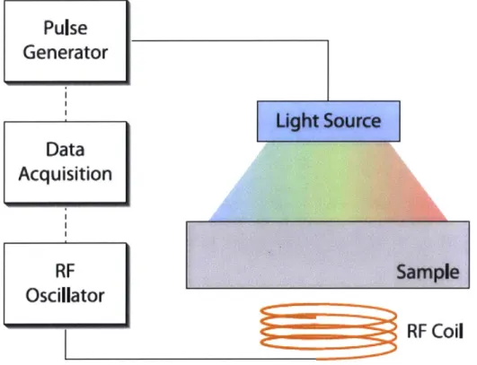
An essential component of optimizing the interface between silicon and tetracene for excitonic transfer is being able to determine the quality of that interface by characterizing the surface states of the silicon. Radio frequency photoconductive decay (RFPCD) is a contactless measurement used to determine minority carrier lifetimes used to measure the nonequilibrium characteristics of the various silicon wafers used throughout this study. First proposed by Miller
[12], the conductance of the wafer is inductively measured by using an radio frequency (RF) coil which acts as the primary of a transformer while the wafer undergoing the measurement is the transformer's short-circuited secondary. A general overview of RFPCD data collection is shown
in Figure 4.
An LED light source above the wafer is used to optically generate excess carriers which increases the conductivity of the wafer. As the conductivity of the wafer increases, a current of corresponding magnitude to the conductivity of the wafer is induced in the RF coil, allowing us to measure the change in the wafer's conductivity as we pulse the light. A power source controls the current driving the LEDs which allows for modulation of the LED light intensity. The data acquisition is triggered by the light pulsing for an amount of time set by the user and gated at 500 microseconds to allow for carrier generation equilibration. The change in excess carrier
concentration with time, which is proportional to the change in wafer conductivity, is given by:
dAn = G - U = Gexternai - A (2.1)
Pulse
Generator
Light Source
Data
Acquisition
Sample
Osciiiator
RF
Coil
Figure 4. Schematic of RFPCD signal flow. The RF coil generates eddy currents that are affected by the sample's conductivity generated by the light source. The pulse generator pulses the light on and off while the data acquisition is triggered and the sample's conductivity is measured by the software. [6]
An LED light source above the wafer is used to optically generate excess carriers which increases the conductivity of the wafer. As the conductivity of the wafer increases, a current of corresponding magnitude to the conductivity of the wafer is induced in the RF coil, allowing us to measure the change in the wafer's conductivity as we pulse the light. A power source controls the current driving the LEDs which allows for modulation of the LED light intensity. The data acquisition is triggered by the light pulsing for an amount of time set by the user and gated at 500 microseconds to allow for carrier generation equilibration. The change in excess carrier concentration with time, which is proportional to the change in wafer conductivity, is given by:
dt = G - U = Gexternai - A (2.1)
RF
where g is the generation rate due to the LED light source. If the illumination were kept constant during excitation (Gexternai = g) then
An = gT(1 - e1).
After illumination is removed (the light pulse ends and), g = 0 and
An = gret/.
(2.2)
(2.3) The T in the above equations is the characteristic time decay constant of the carriers, or the minority carrier lifetime before recombination occurs. Figure 5 illustrates the RFPCD signal and its dependence on the generation rate, g, and r, the effective carrier lifetime.
Light On
g7-
A0
Light Off
gT
exp(-t/r)
Time
Figure 5. RFPCD signal. Conductivity increases when the light pulse is on and carriers are generated. Conductivity, and thus, generation, plateau at a value of gr. The light pulse turns off and the conductivity decays as carriers recombine. The time constant of the decay is characteristic of the minority carrier recombination lifetime in the sample. [6]
However, the effective lifetime measured contains contributions from both the bulk and surface recombination times.
C
C)
U)
0
1 - 1 +-1 (2.4) Teff Tsurface Tbulk
For bulk lifetimes greater than 1 ms, the contribution of the bulk to the effective lifetime is negligible. Thus, minority carrier lifetime measured is the time it takes carriers to recombine at the surface. The Baldo group has estimated that the exciton will undergo tunneling from tetracene to silicon within the first 10 nm of the silicon surface. [6] Thus in this work we are primarily concerned with the requirements of the surface recombination lifetime and surface recombination velocity to ensure exciton transfer.
2.2 SRV requirements
RFPCD ideally measures the number of generated carriers. While one would expect the RFPCD signal to increase if exciton transfer is occurring between tetracene and silicon and stay the same if it isn't, the sensitivity of the system to noise mandates that we set a few requirements for sample parameters that determine successful transfer. Neil Patel, PhD '16 MIT, developed the model for SRV requirements based on internal quantum efficiency of the solar cell. The internal quantum efficiency (IQE), is defined as:
IQE = # of collected carriers (2.5)
# of absorbed photons
and represents the generated carriers who have successfully diffused to the junction, or been collected before they've recombined and thus become useless and impossible to be collected. The IQE is generally highest for wavelengths where carriers are generated within a diffusion length of the junction. The larger the wavelength, the further away from the junction the carrier is which means it has to diffuse for a lot longer before being collected so there's a higher likelihood it will find a majority carrier with which to recombine. Thus, the IQE decreases for longer wavelengths.
the penetration depth of the light so the carriers are generated nearer the surface. The closer the carriers are to the surface, the more likely they are to undergo recombination due to defects at the surface and thus avoid collection which leads to the decrease in IQE. [13]
The bandedge of tetracene is about 530 nm. In order to reap the benefits of tetracene coated silicon, we would expect that carriers generated within 10 nm of the surface of the silicon have an IQE of at least half that of silicon at 530 nm. If 100% of the carriers generated by tetracene were collected, we would see double the IQE of the bulk for 530nm due to singlet fission. Unfortunately for all the of the species on planet Earth, it is much more likely that the transfer yield of excitons is less than 100%, which implies that in order to determine that excitons have definitely transferred and have undergone the singlet fission process, we need to see an IQE that is at least larger than what we would see normally for silicon at that wavelength, 530nm. This means that if we had anything larger than the 1:1 ratio of photon to electron-hole pairs, we would know that singlet fission occurred. Thus, a surface carrier (exciton transferred carrier) IQE that is at least greater than half the bulk IQE at 530nm would demonstrate that the ratio of photons to generated electron-hole pairs must be greater than 1:1 and so proves singlet fission occurred.
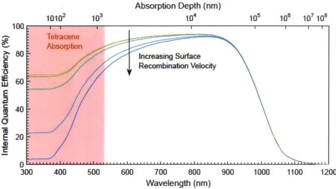
Figure 7 shows the internal quantum efficiency's dependence on SRV (surface recombination velocity) for different wavelengths of incident light and their corresponding absorption depths in Silicon. The greater the SRV, the lower the IQE, because the carriers diffuse much faster to the surface and thus have a higher likelihood of being lost to recombination instead of collected.
Absorption Depth (nm) 10102 1013 105 106"107 10 8 100 110 1 1 Tetracene Absorption > 80 Increasing Surface Recormbination Velocity wJ 6 0 40 20 0 300 400 500 600 700 800 900 1000 1100 1200 Wavelength (nm)
Figure 7. Internal quantum efficiency (IQE) vs wavelength for a typical Si solar cell with front
surface recombination velocities varying from 102 cm/s to 106 cm/s. [6]
The simulation Dr. Neil Patel conducted using PCi D involved a standard solar cell (200 pm thick) with a n-type emitter doped to 4 x 1019 cm-3 and a p-type base doped to 1 x
1016 cm-3 and it assumed there is no surface recombination on the backside. Using Figure 7 and
the IQE requirements discussed above, Dr. Patel modeled the IQE of surface carriers and the IQE from carriers generated at a wavelength of 530 nm as a function of SRV and emitter thickness (Figure 8) and determined that in order for the emitter thickness to remain less than 1 [tm as is ideal, the SRV must stay below 104 cm for efficiency gains to still be seen. Figure 9 plots the IQE of surface carriers minus the IQE at 530 to demonstrate the chances in percentage that would occur in IQE. Taking into account triplet transfer efficiencies for two different emitter thicknesses in Figure 10, Dr. Patel concluded that the SRV should again be at most 104 cm/s to extract the most efficiency gains. Beyond that, the associated lower triplet transfer efficiencies actually reduce efficiency gains. [6]
10 1 0.1 -102 103 104
SRV (cm/s)
10 5Figure 8. IQE for surface carriers (a) and 530nm (b) in a standard solar cell vs emitter thickness (a)
-
100 -80 103 104 105SRV (cm/s)
0 C 0-c
I-0)E
w
60 40 20 0 106 (b) 10 1 Is 1E
w
100 80 60 40 20 0 0.1 ' 1e 10610 -80 60 40 - 1
0
Lij -60 -80 0.1 102 103 104 105 106SRV (cm/s)
Figure 9. IQE of surface carriers generated by singlet fission minus IQE of 530nm in Si. [6] The requirement for SRV to be greater than 104 cm/s in order for exciton transfer to be measured allows us to determine the necessary effective lifetime measurement from RFPCD that satisfies those restraints. The time it takes carriers to recombine at the surface measured with RFPCD which from now on will be called Tsurf and the SRV, S, are related through the transient equation: 1=
#/
2D (2.6) Tsurf Where fl tan( = (2.7)where D is the diffusion coefficient of the minority carriers in the wafer, and d is the wafer thicknesses. If the effective lifetime measured is larger than the time it takes carriers to diffuse to the surface, given by:
1e
SRV (cm/s)
1oe4
SRV (cm/s)
Figure 10. Effect of triplet transfer efficiency and SRV on the change in IQE from surface carriers to IQE minus IQE of 530 nm for a a) 1 prm emitter and a b) 100 nm thick emitter. [6]
100 (a) 0-C
w
1.. 0) 90 80 70 2 60-501 10 10 3ii
(b) 105 106 100 0-w (I) 90 80 . 70 60 501 102 80 60 40 20 0 .-20 .-A0 103 -80 106 - - - --- - - --- - - -- -80 40 40 20 0 -20 -40 -60 -80Tdiff = 2
D(2.8)
where d is the wafer thickness and D is the diffusion coefficient given by:
D = !LkBT (2.9)
q
and [t is the mobility of the minority carrier of the wafer, kB is Boltzmann's constant, T is
temperature, and q is the charge of an electron, then we can say that surface recombination is not rate limited by diffusion. The surface recombination velocity, S, can then be approximated by:
S = d (2.10)
2surf
2.3 RFPCD methodology
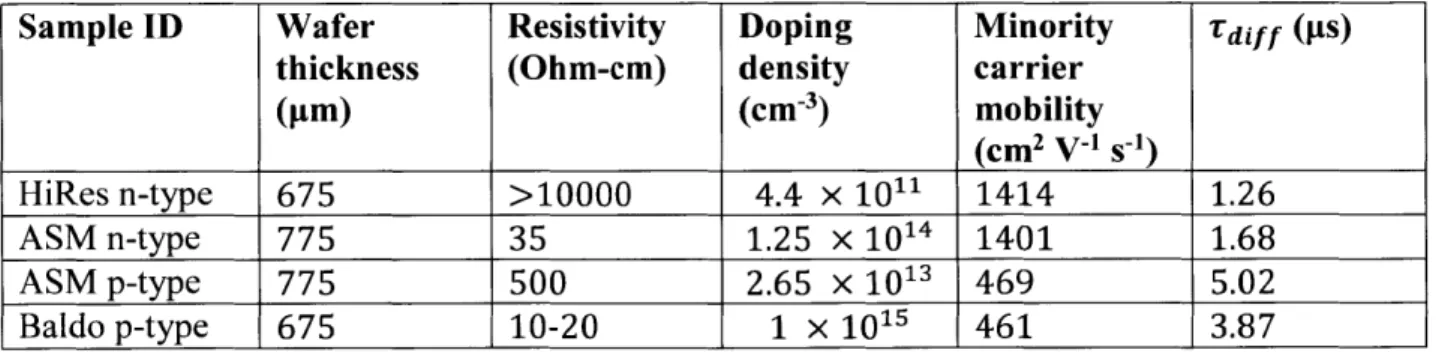
In order to determine the effect of processing on the surface quality of wafers employed in this work, RFPCD was conducted to obtain their effective lifetimes. For each of the wafers employed in this study, the time it would take carriers to diffuse to the surface was calculated to ensure that the measured lifetimes were greater and thus dominated by minority carrier surface recombination rather than diffusion to the surface (Table 1).
Sample ID Wafer Resistivity Doping Minority Tdiff (s)
thickness (Ohm-cm) density carrier
(stm) (cm-3) mobility (cm2 V-1 s-1) HiRes n-type 675 >10000 4.4 x 10" 1414 1.26 ASM n-type 775 35 1.25 x 10⁴ 1401 1.68 ASM p-type 775 500 2.65 x 10' 469 5.02 Baldo p-type 675 10-20 1 x 10¹⁵ 461 3.87
Table 1. Wafers used in this work and their characteristic minority carrier diffusion time.
Because all diffusion times from Table 1 are greater than the measured effective lifetimes and the bulk lifetimes were determined to be less than 1 ms for all wafers involved in the experiment (see
carriers at the surface. The bulk lifetime is so large it has very little influence on the measured lifetime and the lifetime is clearly not diffusion-limited. The SRV is thus inversely proportional to the measured lifetime and so the measured lifetime can be used as a good indication of surface
quality throughout the study.
Each sample was exposed to a 1 ms light pulse (Figure 5). The light pulse was longer than the sample lifetime so that carrier generation could saturate. The RFPCD amplitude would thus be indicative of the generation rate. Data was collected using LabView for long (9000 ps) and short (2000 pis) acquisition times which were then fit to a double and single exponential model, respectively, using Matlab. While the long pulse wasn't long enough to give an accurate indication of bulk lifetime, the long acquisition time substantiated the claim that the short lifetime measured was the lifetime of carriers at the surface by demonstrating goodness of the double exponential fit. The short acquisition time where the signal was cut off at 2000 ps was used to obtain more points along the fast decay for a more accurate measure of the lifetime of carriers at the surface. Figure 11 is an example of a typical decay fit using Matlab.
Single exponential: A exp(-B - x) + C, Tsurf = (2.11)
1
B
Double exponential: A exp(-B - x) + C exp(-D I x) + E, Tsurf = ' Tbulk~ (2.12)
Not only was RFPCD used to determine the lifetime of carriers at the surface and thus the SRV, but the amplitude from RFPCD is proportional to the generation rate of carriers (section 2.1) and so can be used to determine whether or not energy transfer has occurred. Samples were first measured out of the box with no surface prep, then after an RCA clean, then after deposition of tungsten nitride (WN) used to improve tetracene adhesion, and finally after tetracene deposition. The RFPCD measurements prior to tetracene deposition were used to establish a baseline
HiRes Sample 1-2 Bare Single Exponential 0 .1 I I I I 0.09 0.08 0.07 0.06 0 004 .0871 exp(-.0242x)+.0040 0.04 - Rsquare = .9983 0.03 -0.02 -0.01 -0 100 200 300 400 500 600 700 800 900 1000 Time ([s) (a)
HiRes Sample 1-2 Bare Double Exponential
0.1 0.09L 0.08 0.07: 0.06 0) 0.05 0.04 0.0873*exp(-0.0245x)+0.001 6*exp(-0.0005x)+0.0028 0.03 Rsquare = .9963 0.02 0.01 0 0 1000 2000 3000 4000 5000 6000 7000 Time ([Ls) (b)
Figure 11. Example of a single (a) and double (b) exponential fit of the same sample using Matlab. RFPCD signal to decrease from tetracene's absorption of light which can be estimated from the
The samples were measured using 470 and 850 nm light. Silicon absorbs both these wavelengths of light, but tetracene only absorbs 470nm light. If no energy transfer has occurred,
we would expect the RFPCD signal to decrease from tetracene's absorption of light which can be estimated from the Beer-Lambert law:
1 - = 1 - exp(-ad) (2.11)
10
1(d)
where 1 - is the fraction of absorbed light, d is the thickness of tetracene (20 nm), and a is 10
the absorption coefficient of tetracene. If the generation rate ratio of samples with tetracene to samples without tetracene is larger than the fraction of absorbed light, then we know that energy transfer from tetracene to silicon has occurred.
However, just having a difference in generation rate smaller than the difference due to absorbed light by tetracene does not indicate that triplet energy transfer has occurred, specifically. Energy transfer could have been singlet energy transfer only which would generate one electron-hole pair in silicon per tetracene singlet. In order to determine whether triplet energy transfer has occurred, the generation rate ratio of samples with tetracene to samples without tetracene must exceed 1 because triplets arise from singlet fission, leading to two electron hole pairs generated in silicon per triplet if triplet energy transfer is occurring. The sample was always placed in the same location relative to the coil and the light source was always the same distance away from the sample to control for as many variables affecting generation of carriers as possible. Additionally, the spot size of light was uniform along the size of the sample so that all parts of the sample were illuminated evenly. The samples were measured with 470 nm and 850 nm light as an additional control. Because tetracene has no absorption of the 850 nm light, we would expect to see no change in generate rate for samples with and without tetracene. 470 nm light has tetracene absorption so we would expect to see a generation rate decrease if the light is absorbed by tetracene and triplet energy transfer is not occurring or a generation rate increase if triplet energy transfer to silicon is
indeed occurring. Figure 12 demonstrates the predicted signal differences one would observe for the scenarios outlined above.
- - - - - - No Tetracene -ng
- --
With Tetracene C: Transfer (U ' TetraceneCY)
Absorption LLCC
Time
Figure 12. We would expect the amplitude of the RFPCD signal (the generation rate) to increase with triplet energy transfer and decrease if tetracene absorbs the light and triplet energy transfer is not occurring. [6]
2.3.1 RFPCD methodology validation
As this work serves as a continuation of Dr. Patel's preliminary work, the experimental set-up and Matlab script were verified by taking measurements of Dr. Patel's samples and comparing the results of my data collection with his. The samples used for methodology validation have an SiO2 layer on the surface. If the surface is perfectly passivated by the oxide, we would assume the surface quality has not changed. Table 2 details the sample I measured, and the lifetimes obtained when I fit Dr. Patel's data of the sample with my own data of that sample. There are two lifetimes for each sample indicative of the double exponential model these samples obey. Despite one low percent difference of 73.9%, the remaining percent differences between the Patel
and Postelnicu measured lifetimes are all around 80% or higher. Because the thinner 50 nm oxide is subject to faster degradation, it is reasonable that the thinner 50 nm oxide exhibits a greater percent change in measured surface recombination lifetime. The high percentage correlation between the two independent measurements indicate the methodology I have described and followed throughout the thesis is sound.
Sample A (nm) Patel Patel Postelnicu Postelnicu Percent
lifetimes (ps) R2 lifetimes (ps) R2 change
50 nm SiO2 on 850 113.5 0.9999 143.0 0.9995 0.7390 FZ Si 6inch 5095 5762 0.8692 60Amps 470 123.9 0.9999 143.0 0.9995 0.8458 5537 5576 0.9930 100 nm SiO2 on 850 139.3 0.9996 168.1 0.9991 0.7933 FZ Si 6inch 4763 4997 0.9508 60Amps 470 171.8 0.9997 168.5 0.9991 0.9808 5436 4832 0.8888
Table 2. Comparison of measured lifetimes from Dr. Patel's data and Postelnicu's data collection.
2.4 RFPCD baseline results for wafers with no surface prep
In order to obtain tetracene-coated silicon wafers to study the potential for triplet energy transfer between tetracene and silicon, the wafers undergo several processing steps. The first step is an RCA clean (see chapter 3), followed by atomic layer deposition (ALD) of tungsten nitride
(WN) that acts as a glue layer between silicon and tetracene, and finally, evaporation of tetracene.
The wafers were first measured straight out of the box, with no surface prep, to construct the baseline of comparison for the rest of the processing steps. Table 3 summarizes the results for sample when measured with 850 and 470 nm light for short and long acquisition times then fit with the single and double exponential model described in section 2.3. Only the time it takes carriers to recombine at the surface, Tsurf, is reported. The bulk lifetimes are large enough
(Chapter 3) such that the indication of surface quality, SRV, is proportional to lifetime of carriers at the surface alone. Low R2 values resulting from noisy measurements are omitted from this
analysis due to the sensitivity of RFPCD. Thus, only fits with a 95% or greater R2 value are
considered. All of the measurements of bare wafers that have above a 95% R2 value fall within the
range of 40 to 115 ps, which corresponds to a range in SRV of 300 cm/s to 1000 cm/s. Sample Wavelength Injection tsur (us) R2 Exponential
level (Amps)
HiRes Sample 1-2 850 70 40.87 0.9963 Single
850 70 41.36 0.9983 Double
470 66 46.68 0.9628 Single
470 66 54.64 0.9601 Double
HiRes Sample 1-3 850 70 41.16 0.9978 Single
850 70 39.76 0.9967 Double
470 66 44.43 0.988 Single
470 66 45.83 0.9814 Double
ASM n-type 850 70 52.43 0.9932 Single
Sample 11-1 850 70 53.83 0.9196 Double
470 66 172.9 0.5452 Single
470 66 80.55 0.3769 Double
ASM n-type 850 70 48.75 0.9336 Single
Sample 12-2 850 70 50.60 0.9853 Double
470 66 139.6 0.2453 Single
ASM p-type 850 70 46.69 0.9123 Single
Sample 16-2 850 70 45.22 0.9796 Double
470 66 51.63 0.1015 Single
ASM p-type 850 70 45.75 0.9933 Single
Sample 16-3 850 70 44.84 0.9624 Double
470 66 121.2 0.3210 Single
470 66 136.0 0.1569 Double
Baldo p-type 850 70 101.1 0.9985 Single
850 70 99.95 0.9989 Double
470 66 114.8 0.9985 Single
1 _ _ 470 66 114.6 0.9987 Double
Table 3. Lifetimes of carriers at the surface taken with 850 and 470 nm light and fit with single and double exponentials for short and long measurements, respectively, of the decay.
While the resulting SRV from wafers with no surface prep should result in efficiency gains from triplet energy transfer, a lower SRV would still drastically increase those gains - thus motivating the need for surface cleaning and passivation. The bare Si surface has Si atoms with one or two unused valence bonds, termed 'dangling bonds' which can act as traps for carriers and increase the rate of surface recombination. Natural oxide formed by oxygen as well and impurities like metals on the surface also contribute to surface states that increase the rate of surface recombination [10]. The R2 value is always lower for measurements taken using 470 nm light as
the signal is noisier for that wavelength. This may be because the penetration depth of 470 nm light is lower than 850 nm light and thus carriers are generated closer to the surface. The closer to the surface carriers are generated, the more they are subject to recombination. The faster recombination occurs, the lower the signal level of the sample due to the amplitude's dependence on T. The faster recombination occurring closer to the surfaces means lower recombination times for 470 nm light than for 850nm light. Thus, the lower 470 nm signal is closer to the noise level of the system (~.005 V). The samples that experienced very low R2 values had signals close to this
noise level, but the bare surface lifetime resulting from the rest of the samples still falls within these large confidence intervals.
Every effort was made to use the same sample through the process flow described above. However, at times this was impossible as certain cleaning steps had to be conducted within the same environment as and be follow by immediate deposition. The effect of location among the wafer was surveyed for the ASM n-type and ASM p-type wafers. Figures 13 and 14 show the cleaving map for each 2 in. x 2 in. sample that was used in the study. There was no statistically significant difference of lifetime measurement based on location for either the ASM n-type or
ASM p-type wafers (Table 4), thus we can assume a low margin of error for lifetime comparisons of different samples throughout future processing steps.
7
9 10 11 12
5 6 7 8
1 2 3 4
Figure 13. ASM n-type wafer sample map
14 15 16
(
k
x
x
10 5 1 11 6 2 12 7 3 13 81~
I
Figure 14. ASM p-type wafer sample map 14
Sample Wavelength Injection n-type tsui n-type R2 p-type tsurf p-type R2
level (Amps) (us) (us)
1 850 150 54.00 0.9964 46.46 0.9984 470 70 121.1 0.8951 51.58 0.9432 2 850 150 51.88 0.9965 45.94 0.9983 470 70 106.51 0.889 85.06 0.5687 3 850 150 49.09 0.9979 45.61 0.9982 470 70 62.91 0.7786 79.32 0.4494 4 850 150 51.76 0.9972 470 70 140.9 0.8976 5 850 150 51.76 0.9972 45.74 0.9983 470 70 100.7 0.8651 90.39 0.5185 6 850 150 51.16 0.9968 44.88 0.9983 470 70 121.7 0.9012 66.42 0.5627 7 850 150 50.73 0.9967 46.54 0.9985 470 70 130.7 0.878 55.42 0.5549 8 850 150 50.73 0.9967 45.41 0.9984 470 70 103.1 0.9093 77.74 0.441 9 850 150 52.83 0.9969 470 70 103.7 0.8884 10 850 150 52.27 0.9972 47.31 0.9988 470 70 113.7 0.8827 61.19 0.568 11 850 150 51.81 0.997 42.50 0.9978 470 70 103.3 0.8858 84.37 0.597 12 850 150 53.35 0.9963 46.62 0.9979 470 70 103.5 0.8702 80.04 0.5486 13 850 150 52.83 0.9969 45.66 0.9982 470 70 104.9 0.9096 87.02 0.4778 14 850 150 53.90 0.9961 44.84 0.9982 470 70 105.8 0.8893 102.7 0.5462 15 850 150 52.70 0.9968 46.02 0.9981 470 70 100.4 0.8583 105.5 0.5369 16 850 150 54.66 0.9963 45.50 0.9986 470 70 110.7 0.8782 125.6 0.3961
Table 4. ASM n-type and p-type sample measured with both 850 and 470 nm light.
surface lifetimes, fit using a single exponential and
We see again a general trend for lower R2 with the 470nm light due to lower signal as the
signal penetration depth is lower. However, while the p-type values for lifetime measured under
light, the n-type values measured under 470 nm light (~100 pts) are about twice as large as those measured under 850 nm light (~50 pts). One would expect the lifetime of carriers at the surface to increase as the carriers near the surface and interact with more recombination sites. Perhaps a natural oxide at the surface is causing this increase nearer the surface while the surface underneath is still dirty and unpassivated leading to the lower lifetime measurement of 50 pts.
Chapter
3:
Effect
of surface
treatment
on
recombination time and surface recombination
velocity in Silicon
3.1 Background on HF passivation
When a silicon wafer is placed in Hydrofluoric acid (HF), any oxide is removed and the surface is F-terminated. Fluorine weakens the silicon surface back bonds so that Hydrogen can come in and bond to the silicon, resulting in an H-terminated surface. Hydrogen thus saturates the dangling bonds responsible for recombination at the surface, allowing us to measure bulk lifetime using RFPCD. [10]
3.1 RCA clean
The RCA (Radio Corporation of America) clean is one of the most common cleaning procedures for silicon and a necessary step before HF passivation as described above as well as
in the tetracene deposition by the Baldo group. The first step of the RCA clean is called Surface Clean 1 (SC 1) and is a mixture DI water, ammonium hydroxide, and hydrogen peroxide in a
5:1:1 ratio. The second step is called Surface Clean 2 (SC2) which is a mixture of DI water, hydrogen chloride, and hydrogen peroxide in a 6:1:1 ratio. A dilute HF dip may or may not
follow SC2. The solutions are heated to 80'C and the samples are left in SCI for 10 minutes, rinsed with DI water, left in SC2 for 10 minutes, then removed and rinsed with DI water.
SC 1 removes particles and organic compounds from the surface but leaves behind metallic contaminants due to the low solubility of metals in the SC 1 solution which precipitate out as metal oxides. SC 1 also roughens and etches the surface. SC2 removes the metal
complexing to C1 and the presence of H' keeps metals in solution as ions and away from forming solids on the wafer surface. SC2 leaves a thin chemical oxide on the surface. The optional HF dip removes this oxide and leaves the surface hydrophobic. [10]
3.2 HF methodology
The samples were RCA cleaned to remove contaminants from the surface as described in Section 3.1 and then RFPCD was conducted while the samples were immersed in HF. The RFPCD equipment was moved to a hood and a Teflon beaker was placed on top of the coil. Teflon film covered the LEDs to protect them from the HF fumes. The sample was placed in the beaker and just enough HF was used to cover the sample completely. The sample's lifetime was measured using RFPCD and then the sample was rinsed with DI water and blown dry with nitrogen. Because the surface is very nearly perfectly passivated by HF, the SRV tends to 0 and the lifetime measured with RFPCD has the most contribution from the bulk lifetime rather than the surface lifetime.
3.3 Bulk lifetime results
HF passivation and subsequent bulk lifetime results from conducting RFPCD while samples were immersed in HF was used to confirm that the bulk lifetimes of all of the wafers employed in this work were larger than 1 ms such that the non-HF RFPCD was indicative of the lifetime of carriers at the surface. Figure 15 demonstrates the clear difference between the RFPCD signal of a non-HF passivated surface and complete HF passivation. The HF passivation measures the bulk lifetime, which is over 1 ms, and so never fully saturates for the I ms long light pulse employed during the measurement. The ramp-up to the plateau of generation rate is much longer as the recombination rate at the surface is almost 0. The decay is also much slower than the initial
decay measured without the samples immersed in HF. Table 5 summarizes the bulk lifetimes and resulting surface lifetime errors for all the wafer employed in this work except for the Baldo p-type. As 2-4 is is within the noise of the equipment, the effective lifetime serves as a good indication of the surface lifetime.
HiRes Sample 1-1 HF bJ 0 (a) 1.4 1.2 1 0.8 0.6 0.4 0.2 0 -0.2 0 20C 0 4000 6000 8000 10000 Time (ps)
Hi-Res Sample 1-2 without HIF
0 2000 4000 6000
Time (pts)
8000 10000
Figure 15. The plots demonstrate a sample from the same wafer, HiRes, measured while immersed in HF (a) and while measured normally, in air (b). The exponential decay is much slower and longer while measuring the bulk lifetime in (a) in comparison to the sharp initial decay of (b).
tw 0.1 0.09 0.08 0.07 0.06 0.05 0.04 0.03 0.02 0.01 0 (b)
Sample Wavelength Injection tbulk(us) R2 Error in surface
level (Amps) lifetime (us)
HiRes Sample 850 150 2349 0.9972 2.7 1-1 ASM n-type 850 150 1393 0.9989 4.4 Sample 12-1 ASM p-type 850 150 2336 0.9979 2.6 Sample 16-1
Table 5. Measurement of bulk lifetimes and resulting overestimation in surface lifetime when taking the effective lifetime to be the surface lifetime.
3.4 Effect of RCA clean on surface lifetime
Effect of RCA clean on SRV
1000 900 800 700 600 500 -o-HiRes n-type -0-ASM n-type -.- ASM p-type -o-Baldo p-type 400 300 200 100 0
Bare RCA only
Figure 16. Effect of RCA clean on SRV using 850 nm measurements. RCA clean improved the surface quality of all wafers except for Baldo p-type, which aready had a low SRV thus a good surface.
The first step in silicon processing for tetracene deposition is an RCA clean to remove contaminants from the surface. For all of the wafers except the Baldo p-type, the RCA clean improved the surface quality (Figure 16). Only the lifetimes obtained using 850 nm light are
V)
E
LI
reported in Figure 16 as they had a consistently higher R2 value than the 470 nm measurements
and some of the 470 nm measurements were just noise and thus impossible to use.
The RCA clean was expected to improve the surface quality and thus lower the SRV as it rid the surface of impurities that could act as carrier traps and recombination centers. Perhaps the Baldo p-type's surface was already very good and only made worse by any contaminants the RCA deposited or by thin the chemical oxide deposited by the RCA clean. The Baldo p-type also had the highest doping, 10"5, of all the wafers, which may also contribute to the difference in the effect of RCA.
Chapter 4: Effect of Tetracene and Tungsten
nitride on recombination time and surface
recombination velocity in Silicon
4.1 Atomic layer deposition of Tungsten nitride
Tungsten nitride (WN) is used as a glue layer between silicon and tetracene and deposited using Atomic Layer Deposition (ALD) immediately after the silicon is RCA cleaned. The Baldo group graciously conducted the RCA clean and ALD for this work. ALD uses binary reaction sequences where two self-limiting surface reactions proceed in a sequential fashion allowing for precise thickness control of the deposited thin film. Not only can the thickness of thin films deposited through ALD be controlled at the atomic level, but the self-limiting reactions also result in very uniform and smooth layers. [14]
4.2. Evaporation of Tetracene
Following W-N ALD, the tetracene is evaporated onto the surface using a thermal evaporator by the Baldo group. The thermal evaporation occurs in a vacuum chamber with a deposition pressure of less than 3 x 10⁻⁶ torr at a rate between 2 and 4 angstroms per second. The substrate holder was also rotated during the evaporation to result in a more uniform thickness. The thermal evaporator was also directly attached to a nitrogen glovebox where the tetracene-coated samples were encapsulated using UV curing epoxy and a quartz slip to prevent
4.3 Methodology
The Baldo group conducted the deposition of both WN and tetracene with a few difference processing steps so that we could analyze the effect of each of the processing steps the samples underwent on the lifetime of carriers at the surface. The process flows were: 1) RCA with no HF dip then tetracene deposition, 2) RCA with no HF dip followed by WN ALD and then tetracene evaporation, and 3) RCA with an HF dip followed by WN ALD and then tetracene evaporation. Because the ALD required an RCA clean immediately before the ALD took place, we were unable to measure the same sample after RCA clean as well as after the WN deposition. Thus, one process flow includes only the effects of RCA which are considered to be fairly uniform among the wafer (see Section 2.4) and so can be attributed to the other process flows as well. The other process flows measure lifetime before any surface prep, and after RCA + HF +WN or RCA + WN when HF is not used as the last step in the clean. The measurements took about 30 minutes to conduct after each cleaning or deposition process, so some of the results may be affected by degradation of the RCA clean. The WN layer is stable for at least an hour, and the tetracene-coated samples were encapsulated and thus less susceptible to immediate degradation.
4.4 Effects of HF, Tungsten nitride, and Tetracene on surface lifetime
The RPFCD lifetime measurements were conducted and fit using a single and double exponential model using 850 and 470 nm light. The reported SRVS were calculated from the recombination time of carriers at the surface and plotted in Figures 17-20. The 850 nm single exponential fit was plotted for each processing step as the single exponential fit is more precise for surface recombination time. The 470 nm light resulted in very poor signal after a few of the processing steps and thus was not informative for lifetime trends.
Effect of tetracene on SRV of RCA-cleaned wafers 1000 900 800 700 600 500 400 300 200 100 0
Bare RCA only RCA+TET
Figure 17. Effect of RCA clean and tetracene (Tet) deposition with no other HF dip or glue layer of WN on SRVs for 850 nm measurements.
Effect of WN and tetracene on SRV
-+-HiRes n-type
-- ASM n-type
-- ASM p-type
-"--Baldo p-type
RCA + WN RCA+WN+Tet
Figure 18. Effect of tungsten nitride and tetracene (Tet) deposition on surface quality of RCA--.- HiRes n-type -*-ASM n-type -.- ASM p-type Baldo p-type E E 1000 900 800 700 600 500 400 300 200 100 0
Bare RCA only