HAL Id: hal-00672568
https://hal.archives-ouvertes.fr/hal-00672568v2
Submitted on 13 Mar 2012HAL is a multi-disciplinary open access
archive for the deposit and dissemination of sci-entific research documents, whether they are pub-lished or not. The documents may come from teaching and research institutions in France or abroad, or from public or private research centers.
L’archive ouverte pluridisciplinaire HAL, est destinée au dépôt et à la diffusion de documents scientifiques de niveau recherche, publiés ou non, émanant des établissements d’enseignement et de recherche français ou étrangers, des laboratoires publics ou privés.
Optically optimal wavelength-scale patterned ITO/ZnO
composite coatings for thin film solar cells
Antoine Moreau, Rafik Smaali, Emmanuel Centeno, Christian Seassal
To cite this version:
Antoine Moreau, Rafik Smaali, Emmanuel Centeno, Christian Seassal. Optically optimal wavelength-scale patterned ITO/ZnO composite coatings for thin film solar cells. Journal of Applied Physics, American Institute of Physics, 2012, 111, pp.083102. �10.1063/1.3703670�. �hal-00672568v2�
Optically optimal wavelength-scale patterned ITO/ZnO
composite coatings for thin film solar cells
Antoine Moreau,1, 2, 3 Rafik Smaali,2, 3 Emmanuel Centeno,2, 3 and Christian Seassal4, 5 1Center for Metamaterials and Integrated Plasmonics,
Duke University, Durham, North Carolina 27708, USA
2Clermont Universit´e, Universit´e Blaise Pascal,
Institut Pascal, BP 10448, F-63000 Clermont-Ferrand
3CNRS, UMR 6602, IP, F-63171 Aubi`ere
4Universit´e de Lyon, Institut des Nanotechnologies de Lyon (INL),
UMR 5270 CNRS-INSA-ECL-UCBL
5Ecole Centrale de Lyon, 36 avenue Guy de Collongue, 69134 Ecully Cedex, France
Abstract
A methodology is proposed for finding structures that are, optically speaking, locally optimal : a physical analysis of much simpler structures is used to constrain the optimization process. The obtained designs are based on a flat amorphous silicon layer (to minimize recombination) with a patterned anti-reflective coating made of ITO or ZnO, or a composite ITO/ZnO coating. These latter structures are realistic and present good performances despite very thin active layers.
I. INTRODUCTION
Thanks to the maturity of nanophotonics, various advanced light trapping schemes suited to photovoltaic (PV) solar cells have been proposed and investigated in the recent years. The interest of these novel approaches is to generate highly efficient anti-reflecting structures[1– 7], but also, and maybe more importantly, to increase significantly the absorption efficiency in the long wavelength range - where active media are generally less efficient - and finally to reduce the thickness of the absorbing layers. Different groups have been focusing on the possibility to pattern the absorbing layers like crystalline or amorphous silicon[8–11]. This leads to a high absorption enhancement, but the positive impact on the conversion efficiency is still to be assessed. Indeed, the increased area corresponding to the free and processed surfaces may lead to extensive surface recombination. Moreover, the designs generally result from simple design rules, or geometrical parameters scanning. There is therefore a strong need to develop more advanced methodologies, in order to optimize the design of these advanced solar cells. In this paper, our goal is (i) to propose a design methodology based on a purely numerical optimization, guided by a physical analysis, that would be able to make locally optimal structures emerge from the process (ii) to provide designs for solar cell structures including an anti-reflective layer patterned as a photonic lattice, and compatible with a low level of surface recombinations, using the previous methodology.
Here we will consider both flat and periodically patterned anti-reflective coatings made of ITO and ZnO, the two most common materials used as transparent conducting electrodes. We carry on a thorough study of the simplest structures and use genetic algorithms guided by our physical analysis to optimize grating structures. This will lead us to propose hybrid anti-reflective coatings made of ITO and ZnO, to combine the optical properties of ZnO (which exhibits a high refractive index and a low absorption coefficient[12]) with the electrical properties of ITO (which is more conductive, but also more absorbent). The structures we propose are finally very thin (typically thinner than 300 nm) but present surprisingly good efficiencies. These structures can thus be considered as an extremely efficient way to use silicon to convert light into electron-hole pairs and may be relatively inexpensive to produce.
II. FLAT ANTI-REFLECTIVE COATINGS
The goal of this first part is to look for very simple but optically optimal structures and to understand the physical reasons why these structures are locally optimal. This will allow us to guide the numerical optimization of the more complex structures that will be studied in section III.
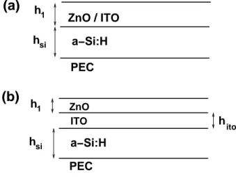
In this first part, we will consider flat anti-reflective coatings made of ZnO or ITO (as shown in figure 1 (a)), or bi-layers hybrid coatings with an ITO layer for electrical reasons and a ZnO layer on top to improve the optical properties of the coating (see figure 1 (b)). A thickness of 30 nm has been considered for the ITO layer in the case of a hybrid coating. Reducing the ITO thickness down to 30nm, compared to a more standard value around 50-70 nm[13], yields a lower useless absorption in the TCO layer. This reduction is made possible in the case of our hybrid design, since the top ZnO layer will also contributes to the lateral conduction of electrical charges.
The a-Si:H layer stands above a perfect electric conductor for simplicity, and to be able to compare with previous works on this subject[6], some of them being particularly reliable and thorough[3]. h1 hsi h ZnO ITO a−Si:H h h 1 ito si
(b)
a−Si:H ZnO / ITO(a)
PEC PECFIG. 1. (a) Layer of amorphous silicon (of thickness hsi) backed with a perfect electric conductor
(PEC) with a simple layer of ITO or ZnO (thickness h1) as an anti-reflective coating and (b) Hybrid
coating with a thickness for the ITO layer of 30 nm.
The figure of merit in all our work is the short-circuit current under normal illumination. We assume that all the photons absorbed by the silicon are converted into electron-hole
pairs and that all the carriers produced contribute to the current - the recombinations of the electron-hole pairs being minimized when considering a thin enough, flat a-Si:H layer. The short-circuit current can in that case be written
jsc = Z A(λ)dI dλ. eλ hcdλ (1)
where λ is the wavelength, ranging from 375 nm (beginning of the solar spectrum) to 750 nm (above which the a-Si:H becomes transparent), dI
dλ the spectral energy density of the light
source (we have taken an am1.5 normalized spectrum[14]) and A(λ) the absorption of the a-Si:H layer (see Appendix VI for details regarding the numerical computation of the ab-sorption). If all the incoming photons of the considered spectral range were converted into electron-hole pairs, the short-circuit current would be equal to j0 = 23.665 mA/cm2. The
conversion efficiency (CE) is given by the fraction of the incoming photons that are con-verted into electron-hole pairs i.e. CE = jsc
j0.
Figure 2 shows the conversion efficiency of the structure when either ZnO or ITO anti-reflective coatings (on top of a 100 nm thick a-Si:H layer) are considered, as a function of the coating thickness h1. It appears clearly that there is an obvious optimal thickness around
52 nm for ZnO (and 56 nm for ITO) for a 100 nm thick silicon layer. This optimal thickness for the coating is accurate : the efficiency is roughly 20% smaller for a 100 nm anti-reflective coating in both cases. This behavior is universal and does not depend on the thickness of the amorphous silicon layer, even if the optimal thickness slightly depends on the a-Si:H thickness.
For thick ZnO layers, the absorption tends to a limit that is 10% below the maximum (this difference is even worse for thicker silicon layers). For ITO the absorption by the silicon layer is a decreasing function of the thickness due to the absorption by the coating itself. This confirms that thin and higher index anti-reflective coatings are a better solution from an optical point of view[6], as long as the losses can be neglected. But ZnO does not present a very high conductivity, so that it is usually necessary to use very thick ZnO layers[3]. That is obviously detrimental to the optical properties, hence the idea to combine a thin ITO layer with a ZnO layer. The resulting anti-reflective coating presents intermediary optical properties, as shown in figure 2, making this structure a very interesting trade-off.
Let us now study how the absorption could be influenced by the thickness of the a-Si:H layer itself, when an optimal anti-reflective coating is assumed (i.e. for each thickness of the
0 0.1 0.2 0.3 0.4 0.5 0.6 0.7 0 100 200 300 400 500 Conversion efficiency Coating thickness (nm)
FIG. 2. Conversion efficiency as a function of the thickness of an anti-reflective coating made of ZnO (solid line), ITO (dashed line) or hybrid anti-reflective coating of ZnO on top of a 30 nm thick ITO layer (dashed-dotted line). The thickness is the overall thickness of the coating in the hybrid case.
a-Si:H layer, the optimal thickness of the anti-reflective coating is computed and used to find the CE). The results are shown in figure 3. The absorption is not a strictly increasing function of the silicon layer thickness, as long as this thickness is smaller than 300 nm. This means that there are clear local maxima of the CE, and that this thickness should probably not be chosen arbitrarily when it is small.
0 0.1 0.2 0.3 0.4 0.5 0.6 0.7 0.8 50 100 150 200 250 300 350 400
Optimal quantum efficiency
Silicon thickness (nm)
FIG. 3. Conversion efficiency of the structure as a function of the silicon thickness for an optimal coating made of ZnO (solid line), ITO (dashed line) or hybrid anti-reflective coating of ZnO on top of a 30 nm thick ITO layer (dashed-dotted line).
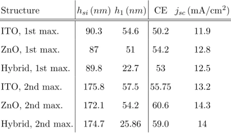
Figure 3 shows three local maxima, whatever the anti-reflective coating. The first two maxima are more pronounced than the third one, and since they happen for small values of the thickness, these maxima correspond to structures making a much more efficient use of silicon - that is especially true for the first maximum, but the second one definitely present a higher efficiency that could be interesting too. The characteristics of these structures are detailed table I. Structure hsi(nm) h1(nm) CE jsc(mA/cm2) ITO, 1st max. 90.3 54.6 50.2 11.9 ZnO, 1st max. 87 51 54.2 12.8 Hybrid, 1st max. 89.8 22.7 53 12.5 ITO, 2nd max. 175.8 57.5 55.75 13.2 ZnO, 2nd max. 172.1 54.2 60.6 14.3 Hybrid, 2nd max. 174.7 25.86 59.0 14
TABLE I. Geometrical parameters of the local optical optima shown in figure 3.
Physically, the efficiency of an anti-reflective coating relies on the resonances it may support : any resonance is associated with a high transmission of light to the underlying medium. If the anti-reflective coating presents an index that is intermediate between the active layer and the superstrate (the superstrate being air, this is the case for ITO and ZnO here), these resonances occur when λ ≃ 4h n
1+2m where h is the thickness and n the index of
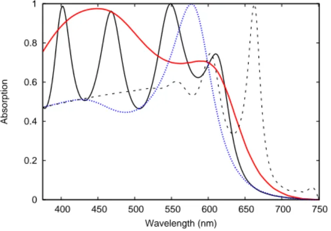
the dielectric layer and m is the order of the resonance. Figure 4 shows absorption spectra for the optimal thickness of a ZnO layer and for a much thicker layer. For thick layers, the resonances are numerous and narrow. Slightly changing the thickness in this regime will just shift the resonances a little, but since the resonances and the anti-resonances will be averaged over the whole spectrum, the change in the thickness has little impact on the overall efficiency. On the contrary, a very thin anti-reflective coating supports essentially one resonance around λ ≃ 4h n(λ). The position of this broad resonance has a great impact on the CE and it can be tuned to maximize the efficiency : the optimal position for the resonance seems to be located where the silicon is the most absorbent. According to the formula above, a thickness of 51 nm should produce a resonance around 435 nm - which is totally consistent with the spectra shown in figure 4. That is why the efficiency is very
sensitive to the thickness of the coating for thin layers, and why thin coatings are more efficient[6]. 0 0.2 0.4 0.6 0.8 1 400 450 500 550 600 650 700 750 Absorption Wavelength (nm)
FIG. 4. Absorption spectra for different structures : a 87 nm thick a-Si:H layer (i) with a 51 nm thick optimal ZnO coating (red curve) (ii) with a 500 nm thick ZnO coating (solid black curve) (iii) without any anti-reflective coating (blue dotted curve) and (iv) a 500 nm thick a-Si:H layer without coating (black dashed curve).
Let us now consider the impact of the silicon layer on the CE. The a-Si:H layer can support cavity resonances when the penetration length is smaller than the thickness. A typical absorption spectrum for a thick layer without any anti-reflective coating is shown in figure 4. For short wavelength (λ < 550 nm), the amorphous silicon is very absorbent and the spectrum is almost flat. Several resonances can be seen on the spectrum for longer wavelength. As discussed already for the anti-reflective coating, these resonances are nar-row because of the layer’s thickness. Any change in the thickness is likely to increase the conversion efficiency, but only slightly. On the contrary, thin a-Si:H layers (compared to the penetration length) may support broad resonances over almost the whole spectrum. As shown in figure 4, a 87 nm thick silicon layer without any coating supports essentially one broad resonance in the middle of the visible spectrum. This resonance still appears as a shoulder on the spectrum of the structure with the optimal anti-reflective coating.
Finally, these carefully optimized cells present good theoretical efficiencies.
Let us consider a typical non-optimized flat structure, also considered in [3]. The structure is a 300 nm thick a-Si:H layer, backed by a 19 nm ZnO layer and a perfect electric conductor, with a 1024 nm thick ZnO coating. According to our simulations, it presents an efficiency
of 53.3% on the range of the spectrum considered here (our simulations are generally in an excellent agreement with all the results presented in Kroll et al.). This structure is typical essentially because, for electrical reasons, it presents a very thick transparent oxide layer.
By comparison, the locally optimal structures we propose are able to reach a similar effi-ciency with much less silicon (three times less silicon typically in this case). This is of course partly due to the optimized anti-reflective coating, and can be seen as an illustration that, as shown in figure 3, it is relatively easy to reach interesting efficiencies with thin active lay-ers, while any further increase of the efficiency may generally require a large supplementary amount of silicon.
III. PATTERNED COATINGS
It is well known that structuring the silicon or the electrode layer can have a great impact on absorption, leading to increased efficiencies. In this part, the impact of the patterning of the anti-reflective coating only on the conversion efficiency is assessed. Our goal is still to find optically (and at least locally) optimal structures with a flat and as thin as possible amorphous silicon layer, to minimize recombination. The structures we consider are shown in figure 5.
The optical behavior of these structures is complex, and their geometry is controled by many parameters. The optimization cannot be done manually as it has been done above. Home-made genetic algorithms[15] were thus used to find parameters corresponding to a maximum conversion efficiency.
Had we just ran an unconstrained optimization, the result would have been a very thick active layer. But the previous physical analysis of the flat structures gives a strong indication that locally optimal structures may exist even for more complex structures. In order to find these local optima, the genetic algorithm has been constrained. Since we expected the optimal patterned structures to resemble somehow the flat ones, we have used different constraints based on the above results. The algorithm was allowed to consider only structures with hsi < 150 nm, or with hsi < 200 nm (or even with hsi < 250 nm).
The algorithm was able to find optimal structures, thus establishing the existence of local optima. The results are summarized in tableII. They show that the patterned optimal structures are very close to the flat ones : the thickness of the active layer is very close in
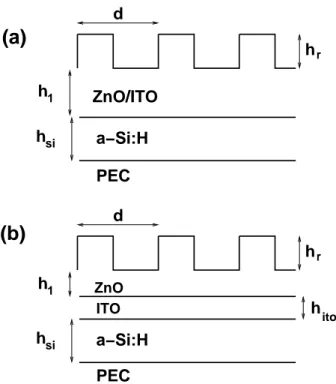
h1 hsi a−Si:H hr d ZnO/ITO PEC
(a)
h ZnO ITO a−Si:H h h 1 ito si hr d(b)
PECFIG. 5. Structured anti-reflective coating. The geometrical parameters are hsi, the thickness of
the silicon layer, d the period of the grating, hr its height and f the fill factor, while h1 is the
thickness of the layer between the silicon and the grating.
both cases, as is the thickness of the homogeneous part of the anti-reflective coating. This is what allows us to conclude that the physical behavior of the structures is still dominated by the phenomena studied in the previous part : the resonances inside the silicon layer and the homogeneous (unpatterned) part of the anti-reflective coating.
Moreover, let us just underline that :
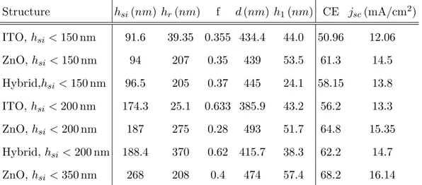
• The patterning is obviously not interesting for the ITO coating : any increase of the ITO thickness is detrimental to the optical properties and the advantages of the patterning are not large enough to overcome that drawback - so that the flat structure seems to be very close to the optimal solution in that case.
• The ZnO coating presents once more the best optical properties. It is possible to compare similar patterned and non-patterned structures. The patterning brings a increase of 13% in the conversion efficiency for the thinnest structure and of 7% for the second maximum.
Structure hsi(nm) hr(nm) f d (nm) h1(nm) CE jsc(mA/cm2) ITO, hsi< 150 nm 91.6 39.35 0.355 434.4 44.0 50.96 12.06 ZnO, hsi < 150 nm 94 207 0.35 439 53.5 61.3 14.5 Hybrid,hsi < 150 nm 96.5 205 0.37 445 24.1 58.15 13.8 ITO, hsi< 200 nm 174.3 25.1 0.633 385.9 43.2 56.2 13.3 ZnO, hsi < 200 nm 187 275 0.28 493 51.7 64.8 15.35 Hybrid, hsi < 200 nm 188.4 370 0.62 415.7 38.3 62.2 14.7 ZnO, hsi < 350 nm 268 208 0.4 474 57.4 68.2 16.14
TABLE II. Short-circuit current and conversion efficiency (CE) for various optimized structures depicted in figure 5.
• The composite coating allows once more to approach the performances of the ZnO coatings. The patterning is responsible for a 10% (respectively 6.2%) increase of the conversion efficiency for the first optimum (respectively the second optimum).
Physically, two mechanisms can explain the efficiency of the grating : (i) it is a sup-plementary layer with a different effective index, making the anti-reflective coating more effective for different wavelength, (ii) it allows to excite guided modes inside the active layer, leading to an enhanced absorption at longer wavelength where the amorphous silicon can be considered almost completely transparent.
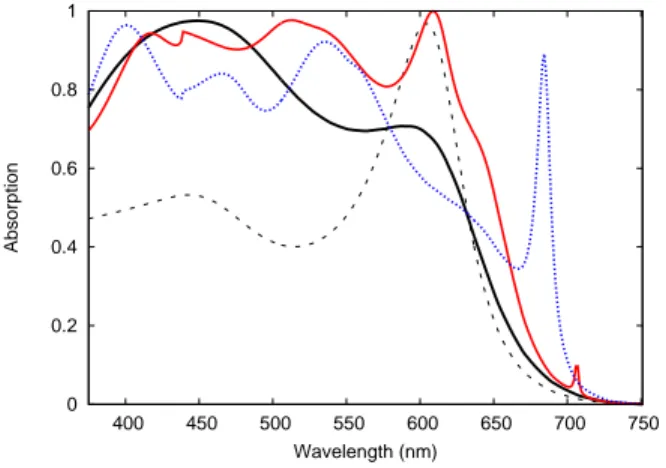
Figure 6 shows the absorption spectrum for the optimal structures with a ZnO coating. The red curves on figure 4 (optimal flat ZnO layer) and figure 6 (optimal patterned ZnO coating) can be compared. The anti-reflective behavior persists in the same way in the blue part of the spectrum. The most obvious difference is the peak that can be seen around 600 nm. This can perfectly be understood if the whole ZnO structure is seen as a double layer optical filter. The numerical method we use (see Appendix and [16]) gives access to the modes propagating inside a ZnO grating layer (corresponding to the first ZnO structure in table II). Two modes are actually propagative : the first one has an effective index of 1.687 at 600 nm, and the second one presents an lower index of 0.1149. The first mode can be considered responsible for the transmission of this layer, the other being slightly excited but the incident plane wave. Adding the grating layer can thus be seen as adding
another homogeneous layer to an optical filter, with a well defined refractive index and a simple simulation[17] shows that the resulting anti-reflective coating presents a transmission peak at 600 nm in TE polarization. This perfectly explains the absorption peak of the structure. There is obviously no absorption peak for the TM polarization, which suggests that a 2D structure could be more effective if it was able to present the same behavior for both polarizations. 0 0.2 0.4 0.6 0.8 1 400 450 500 550 600 650 700 750 Absorption Wavelength (nm)
FIG. 6. Absorption of the first optimum for a ZnO coating (black line), of a 94 nm a-Si:H slab (the black dashed line corresponds to the bare silicon layer) and of the first optimal grating structure (ZnO, hsi< 150 nm ; red line : TE polarization, blue line : TM polarization).
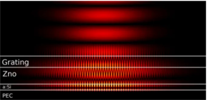
The narrow peaks appearing in the red part of the spectrum are due to guided modes inside the silicon layer excited by the grating. These modes are actually leaky[18]. Figure 7 shows one of these particular resonances, whose position is dominated by the grating period and only marginally affected by the coating thickness. The fact that the field inside the silicon layer extends far from the excitation when illuminating the structure with a beam is a sign that a guided mode is actually excited. The extension of this mode is limited by the contra-directional coupling due to the grating - so that this phenomenon looks very much like a light wheel here[19].
These performances can be compared either to similar optimized structures[3], to cells based on a thin (around 100 nm thick) patterned amorphous silicon layer[5, 6, 8, 9]. It is not always easy to make accurate comparisons (especially when we disagree about the maximum achievable short-circuit current j0[6]). It still appears that the performances of the structures
FIG. 7. Resonance excited in the structure corresponding to the first maximum for a ZnO anti-reflective coating structured layer, at 684.4 nm but for a thickness h1 = 300 nm : this allows to
lessen the coupling between the forward and the backward mode, allowing us to see the spatial extension due to the guided modes better.
cell very similar to our, Kroll et al. reach a 14.4 mA/cm2
(according to our simulations, for the spectral range considered here) with a thick anti-reflective coating and a 338 nm thick silicon layer. According to our results, this performance could have been obtained with a 94 nm thick layer and a very thin ZnO layer instead - but to be fair, we should compare to the composite structure (the thin ZnO layer would not be electrically realistic), that presents a 13.8 mA/cm2
short-circuit current only. And the second optimum is based on a 188 nm thick active layer - but it presents slightly better properties (14.7 mA/cm2). Otherwise, the
absorption spectra of our structures compare very well with cells in which recombinations are much more likely to happen[5, 8, 9], reaching similar performances. Finally, Zanotto et al. see a 12.4% increase of jsc due to a patterning of the active layer that we were able to
attain by patterning the anti-reflective coating only.
IV. CONCLUSION
The thorough physical analysis we have conducted here shows that the resonances occur-ring in very thin solar cells (with a flat active layer of a-Si:H typically thinner than 200 nm and anti-reflective coatings based on a roughly 50 nm thick homogeneous layer of ZnO or ITO) have more impact on the conversion efficiency than for much thicker structures. For these very thin structures, the short-circuit current is for instance not a strictly increasing function of the silicon layer. This means that there are pronounced local maxima of the
conversion efficiency for flat anti-reflective coatings as well as patterned anti-reflective coat-ings (increasing the efficiency of at least 10% for our thinnest structures compared to flat coatings). We have used a genetic algorithm guided by our physical analysis to find these locally optimal structures.
This kind of structures, with a flat and very thin active layer, is particularly interest-ing because (i) the recombinations are minimized, conversely to approaches based on the patterning of the active layer and (ii) it represents a very efficient use of the silicon to convert light into electron-hole pairs. We have actually obtained a short-circuit current of 13.8mA/cm2 for a structure with a 96.5 nm thick only silicon layer (corresponding to a
58.15% conversion efficiency over the 375 to 750 nm range). This structure has a composite anti-reflective coating made of a 30 nm thick ITO layer with a patterned ZnO layer on top of it, which allows to combine the optical properties (high index and low losses) of ZnO with the electrical properties of ITO.
Using the same methodology, more complex photonic patterns can be considered, for example leading to a reduced dependence on the incident light polarization or to an absorp-tion enhancement over a wider wavelength range. This includes 2D patterns or multi-scale structures, for which a simple geometrical parameters scanning is not appropriate to provide a relevant optimization of the design.
V. ACKNOWLEDGMENTS
The authors would like to thank St´ephane Larouche for fruitful discussions and simula-tions concerning the anti-reflective behavior of the grating and R´emi Poll`es for the help for figure 7.
VI. APPENDIX
The absorption inside the active a-Si:H layer is computed using either the scattering matrix method [20] for the flat coating or a Fourier Modal Method[21, 22] for a patterned electrode. The absorption is obtained by the difference between the flux of the Poynting vector at the upper and a the lower interfaces of the silicon layer, when the incident power
is normalized to one. In TM polarization, this flux can be written ΦM = ℜ X n 1 2ωǫ0ǫr γn(A∗n−Bn∗)(An+ Bn) ! , (2)
where Anand Bnare the amplitudes of mode n in the silicon layer (propagating or decreasing
downward and upward respectively), γn =
q
ǫrk02− 2π nd its propagation constant, ǫr being
the permittivity of a-Si:H, k0 the wavenumber in vacuum and d the period of the grating .
In TE polarization, the flux can be written
ΦE = ℜ X n 1 2ωµ0 γ∗ n(An−Bn)(A∗n+ Bn∗) ! . (3)
For a flat structure, the flux is computed considering only the 0th order (n = 0) and there is no need to make any difference between the two polarizations in normal incidence. The conversion efficiency is averaged on TE and TM polarization when the absorption is different for the two polarizations.
[1] C. Haase, H. Stiebig, Appl. Phys. Lett. 91 (2007) 06116.
[2] S.S. Lo, C.-C. Chen, F. Garwe, T. Pertch, J. Phys. D : Appl. Phys. 40 (2007) 754.
[3] M. Kroll, S. Fahr, C. Helgert, C. Rockstuhl, F. Lederer, T. Pertsch, Phys. Stat. Sol. (a) 205 (2008) 1777.
[4] R. Dewan, D. Knipp, J. Appl. Phys. 106 (2009) 074901.
[5] A. Campa, O. Isabella, R. van Erven, P. Peeters, H. Borg, J. Krc, M. Topic, M. Zeman, Prog. Photovolt: Res. Appl. 18 (2010) 160.
[6] S. Zanotto, M. Liscidini, L. C. Andreani, Opt. Expr. 18 (2010) 4260. [7] D. Madzharov, R. Dewan, D. Knipp, Opt. Expr. 19 (2011) A95.
[8] Y. Park, E. Drouard, O. E. Daif, X. Letartre, P. Viktorovitch, A. Fave, A. Kaminski, M. Lemiti, C. Seassal, Opt. Expr. 17 (2009) 14312.
[9] O. E. Daif, E. Drouard, G. Gomard, A. Kaminski, A. Fave, M. Lemiti, S. Ahn, S. Kim, P. R. i Cabarrocas, H. Jeon, C. Seassal, Opt. Expr. 18 (2010) A293.
[11] X. Meng, G. Gomard, O. E. Daif, E. Drouard, R. Orobtchouk, A. Kaminski, A. Fave, M. Lemiti, A. Abramov, P. R. i Cabarrocas, C. Seassal, Sol. En. Mat. Sol. Cells 95 (2010) S32.
[12] Y. Liu, J. Hsieh, S. Tung, Thin Sol. Films 510 (2006) 32.
[13] F.-J. Haug, K. S¨oderstr¨om, A. Naqavi, C. Ballif, J. Appl. Phys., 109 (2011), 084516.
[14] ASTM. Standard tables for reference solar spectral irradiances: direct normal and hemispher-ical on 37◦ tilted surface. Standard G173-03 (American Society for Testing and Materials,
West Conshohocken, PA, 2003), available from: http://rredc.nrel.gov/solar/spectra/am1.5/. [15] D. Goldberg, Genetic Algorithms, Addison Wesley, 1989.
[16] A. Moreau, C. Lafarge, N. Laurent, K. Edee, G. Granet, J. Opt. A : Pure Appl. 9 (2007) 165. [17] S. Larouche, L. Martinu, Appl. Opt. 47 (2008) C219.
[18] A. Moreau, D. Felbacq, J. Europ. Opt. Soc. : Rap. Pub. 3 (2008) 08032. [19] P. Tichit, A. Moreau, G. Granet, Opt. Expr. 15 (2007) 14961–14966.
[20] F. Krayzel, R. Poll`es, A. Moreau, M. Mihailovic, G. Granet, J. Europ. Opt. Soc. Rap. Pub. 5 (2010) 10025.
[21] P. Lalanne, G. M. Morris, J. Opt. Soc. Am. A 13 (1996) 779. [22] G. Granet, B. Guizal, J. Opt. Soc. Am. A 13 (1996) 1019.