BIPOLAR VOLTAGE CONTROL OF A 5 MV VAN DE GRAAFF GENERATOR by
CHARLES DOUGLAS ROLLMAN B.
s.
I LEHIGH UNIVERSITY1971
SUBMITTED IN PARTIAL FULFILLMENT OF THE REQUIREMENTS FOR THE DEGREE OF
MASTER OF SCIENCE at the
MASSACHUSETTS INSTITUTE OF TECHNOLOGY January, 1974
Signature redacted
Signature of Author. . • . . . • . . . . Department of Electrical Engineering, January, 1974
Signature redacted
.
.
. .
.
. . .
.
. . .
.
Certified by Thesis Su ervisorSignature redacted
Accepted by . . . • . . . . Chairman, Departmental Committee on Graduate Students2
BIPOLAR VOLTAGE CONTROL OF A 5 MV VAN DE GRAAFF GENERATOR by
CHARLES DOUGLAS ROLLMAN
Submitted to the Department of Electrical Engineering on January 30, 1974 in partial fulfillment of the requirements for the Degree of Master of Science.
ABSTRACT
A system which provides a means of voltage control of a 5 MV Van de Graaff generator has been designed. The use of bipolar voltage measurement and belt charging techniques in this system results in a unique ability to produce terminal voltage of arbitrary waveform.
For design simplicity, the control system is partitioned into
functional blocks which perform terminal voltage measurement, voltage error correction, and terminal charging. Wideband, bipolar voltage measurement is obtained by combining a synchronous generating volt-meter and a capacitive divider. An error corrector which maintains a very small error between terminal voltage and an input signal, and which also compensates for the long generator time constant has been designed. To permit linear and bipolar belt charging, a circuit
incorp-orating feedback control of a high voltage differential output amplifier is used. Charging circuits located at the terminal and ground ends of the column allow simultaneous control of up and down charge.
Control system performance has been tested using a 2 MV Van de Graaff generator. By connecting a function generator to the input,
.3Hz 500 kV triangular, trapezoidal and sinusoidal terminal voltages have been reproduced with good accuracy. Maximum operating fre-quency is restricted to less than 1 Hz due to belt charge capacity and charge transit delay. DC terminal voltage drift is less than 1 kV and ripple is less than 4 kV.
Thesis Supervisor: Chathan M. Cooke
Professor of Electrical Engineering Title:
3
ACKNOWLEDGEMENT
To Chat Cooke, for his encouragement, constructive criticism and freely given time,
to Hazel Emerson, who typed almost forever, and
to all the people at the High Voltage Research Laboratory, whose friendships I value highly,
Thanks.
Charles D. Rollman January 30, 1974
TABLE OF CONTENTS PAGE Title Page 1 Abstract 2 Acknowledgment 3 Table of Contents 4 1. INTRODUCTION 5 2. DESIGN FEATURES 10 3. BELT CHARGING 12
3.1 Charge Spray Control 12
3.2 Terminal Current Control 21
4. VOLTAGE MEASUREMENT 29
5. VOLTAGE CORRECTION 37
5.1 DC Correction 37
5.2 AC Correction 49
6. CONTROL SYSTEM BLOCK DIAGRAM 50
7. CIRCUITRY DESIGN 52
8. SYSTEM PERFORMANCE 62
9. CONCLUSION 71
5
1. INTRODUCTION
A Van de Graaff generator is a device in which voltage is pro-duced by charge transported to an insulating terminal electrode via a moving belt. Machines of this type are useful in applications requiring production of very high voltages and modest currents within a confined space.
A typical Van de Graaff design is shown in Figure 1. The ter-minal electrode is supported by a column composed of metal equi-potential planes separated by solid insulators. Large value resistors interconnect these planes to insure an even electric field distribution along the column's length. The generator's belt runs through the column between an idler pulley within the terminal and a driving pulley beneath the column. Charge is applied to the belt near the driving pulley and removed at the generator's terminal. Terminal capacitance, column resistance, and belt transport delay comprise the dominant electrical elements and result in the equivalent circuit of Figure 2. Van de Graaff generators of this design are capable of producing several million volts at hundreds of microamperes.
The maximum voltage produced by a Van de Graaff generator de-pends on how well the terminal is insulated. For this reason studies of dielectrics, particularly certain compressed gases which are
especially good high voltage insulators, have been an integral part of the development of these machines. Compressed gases have also been of interest in the electric power industry to facilitate the trans-mission of greater amounts of power through enclosed apparatus of reduced size. Gas insulated equipment for up to 500 kV transmission has been developed and still higher voltages are under investigation. At the MIT High Voltage Research Laboratory, very high and ultra high voltage testing of compressed gases and compressed gas insul-ated transmission lines has been performed using the Van de Graaff
Upper Pulley Terminal Upper Charging Screen -4 -4 Equipotential -. Planes -4 -4 -4 -0 Solid Insulator Column Resistor
Lower Charging Lower Pulley
Screen
Figure 1. Typical Van de Graaff Generator Design Belt Ij '-I Ii. 1 '/1 m - m 'I I., I.-- -(m - -C -I *1 C -C -I' I, C- - -If / C -'II ~~
R C
Terminal "Voltage
CI
Simplified Van de Graaff Generator Equivalent Circuit 7
T
Second Delayt
Ibelt
Figure 2.8
generator as a voltage supply.
Several of the Van de Graaff generator's qualities make it par-ticularly suitable for compressed gas insulation (CGI) studies. Such generators are several times smaller than alternative megavolt sources like transformers or voltage doubler stacks. They are usually insulated in compressed gas and are therefore enclosed by a conducting steel pressure vessel which permits safe observation of multimegavolt phenomena from distances of only a few feet. Elaborate protection devices are not necessary since Van de Graaff generators are current limited by the charge carrying capacity of the belt. They also do not require high voltage rectification or filtering to produce DC voltages.
A disadvantage associated with Van de Graaff generators is the complexity of the equipment needed for voltage control. Unlike magnetic induction in a transformer, electrostatic processes by which voltage is developed are variable and external stabilization
methods are usually required. Control systems which maintain a high degree of DC terminal voltage stability have been designed for use in ion accelerators and for other applications.2,4,5,6,7
During the 1960s a 1.5 megavolt compressed gas insulation test apparatus evolved at the High Voltage Research Laboratory. It consisted of an old Van de Graaff generator previously used as an accelerator, two mating pressure vessels, one enclosing the generator and one for an experimental transmission line section, a control system for the generator, and measurement electronics. Use of this system proved the utility of the Van de Graaff generator in CGI research and also suggested refinements, particularly in control, which could improve system performance.
9
The first Van de Graaff generator control system equipped for AC operation was built as part of the 1969 S.M. thesis work of Armin Diessner at the HVRL. To produce the alternating terminal voltage the charging current polarity was periodicly reversed by a high voltage relay located at the belt charge power supply. An early version, which proved the feasibility of AC operation, employed a variable speed motor with cams that periodicly switched the charge polarity relay. Subsequently, to obtain better control of peak ter-minal voltage during AC operation, a feedback configuration was employed in which the terminal voltage was measured and polarity
switching occurred when it exceeded a desired level.
Diessner's system worked well enough to demonstrate the use-fulness of the AC Van de Graaff generator for high voltage dielectric studies, but also indicated necessary improvements in control. The peak AC voltage was highly sensitive to the timing of polarity
reversal, but the mechanical relays employed by Diessner were not fast or reliable enough for this requirement and voltage variations of ten percent and more were often observed. AC performance also changed with gas pressure and type employed in the experiment due to inadequate belt current regulation. The system was generally difficult to operate.
In 1972, as a preliminary to this thesis, a new control system which employs completely electronic switching was developed and
tested. This system provided the same DC and triangular AC modes of control as the earlier system with much improved reliability and stability.
The success of electronic switching has indicated that the con-trol system for a new test facility, capable of 5 million volts DC and
AC, should be all electronic. This thesis is concerned with the
10
2. DESIGN FEATURES
Several control system characteristics are particularly desirable for compressed gas insulation studies. Accurate and stable voltage measurement and control is required since breakdown phenomena in compressed gas are highly voltage sensitive. System function should be continuous through zero so that no switching is required to change polarity during AC operation. Fast response is also
important to aid in the study of time dependent events. In general, control system versatility should permit its easy adaptation as experiments may require.
A simple block diagram of a possible Van de Graaff generator control system is shown in Figure 3. Voltage control in this design is performed by a feedback loop which measures the terminal volt-age and produces an appropriate error correcting signal to control charging current. Separation of the system into blocks which per-form measurement, error correction, and charging functions, and the linearization of those blocks where possible helps simplify the design problem.
So that DC as well as triangular AC terminal voltages are avail-able, the error correction block in Figure 3 has two modes of opera-tion. In the DC mode it controls belt current as necessary to
minimize the error between the input voltage and the measured ter-minal voltage. For triangular AC operation it maintains a constant belt current magnitude but reverses belt charge polarity each time peak terminal voltage is sensed.
This system design offers a unique advantage over previous ones. Because operation is continuous through zero and because the
function of the DC mode is to maintain minimum error, terminal volt-age will track an arbitrary waveform applied to the input of the DC corrector. This means that sinusoidal AC testing at ultra high
11
voltages can be performed using the Van de Graaff generator.
Error
Correction -InutSignal
Figure 3. Simplified Control System Block Diagram Terminal Voltage Measurement -Belt Charge Control I i Belt Current
12
3. BELT CHARGING
3.1 Charge Spray Control
By providing the critical interface between electronics and the
Van de Graaff generator's terminal voltage, the charging control block reduces the problem of Van de Graaff control to a circuit and electronic system design problem. Because the charge control block is so basic to the control system's function, its limitations,
especially in frequency and charge capacity, are intimately related to the performance of the system as a whole.
Belt charging is accomplished by a method similar to that shown in Figure 4. A voltage difference between a sharp electrode on one side of the moving belt and a blunt electrode on the other side pro-duces an ionizing gradient at the sharp electrode. Depending upon the polarity of the applied spray voltage, ions of one polarity drift due to the gradient towards the blunt electrode and are intercepted
by the belt. Belt movement carries charge on the belt from the
charging region producing a net current flow from the electrodes. Removal of charge from the belt is done in a similar manner, but without need of an applied voltage since charge on the belt will
produce its own gradient in the vicinity of a spray screen.
Design of a belt charging control circuit is complicated by a number of factors. The relationship between spray voltage and the resulting belt current varies with pressure and composition of the
surrounding gas, belt condition, position of the belt as it passes the charging electrodes, charging electrode configuration, and other factors. As a result, fixing the spray voltage at a known level neither guarantees a specific belt current nor that the current
is time invariant. Because the voltage required to produce typical charging currents varies up to 20 kV, belt charge control implies control of a multi-kilovolt source which, due to power dissipation
13 Belt Sharp Electrode ##APO
It
High Voltage Power supply Blunt ElectrodeBelt Charging Technique Figure 4.
14
restrictions, means large impedances and therefore long time con-stants. High charging voltages also complicate measurement of charging current, since direct belt current measurement would imply monitoring current flow to an electrode which floats many kilovolts above ground.
Of the many different charging control schemes which have been
used in Van de Graaff accelerator control systems, two simple ones employing a high voltage triode as the regulating device are the most common. In both of these methods, charge is applied by a voltage difference between a spray screen and the lower pulley of the Van de Graaff generator. For systems operating at negative ter-minal potentials, a series current regulator as shown in Figure 5a is used. For positive belt charge, a shunt regulator is often em-ployed as in Figure 5b. A shunt regulator may also be used to apply negative belt charge by grounding the spray screen and controlling a positive voltage at the pulley. Often a feedback loop within the charging circuit helps stabilize belt current. None of these schemes permits the application of an arbitrary polarity of belt charge.
The design features discussed earlier places two requirements on the charging circuit: linearity and continuity of operation through zero belt current. Since linearization can be performed by enclosing the charging circuit in a feedback loop, only the continuity of con-trol at zero current represents a major design problem. Belt current is monotonicly related to the voltage difference between the charg-ing electrodes; therefore, the problem of bipolar chargcharg-ing control is equivalently a problem of bipolar voltage difference control.
An obvious means of providing the desired charging character-istics would be to devise a controllable high voltage source capable
of applying positive or negative voltages to a spray screen opposite
'belt
AA"A
Figure 5a. Belt Charging Scheme For Negative Terminal
Figure 5b. Belt Charging Scheme For Positive Terminal 'belt t I ~
9
71
20kv Supply A 4 4 0 20kv Supply~~1
C71 'belt 'beltsource proves to be complex and inefficient in terms of power supply usage.
An alternative approach is to use the difference voltage between two controllable positive voltage sources to produce the required charging gradient. Such a method avoids the problems of trying to control a large negative voltage, but still permits gradients of either direction, and thus charge currents of either polarity. One realiza-tion of this approach is to use a pair of high voltage triodes in a differential output amplifier configuration (Figure 6). Such a design
is simple, easily analyzed, easily controlled, uses a single high voltage power supply and performs the desired function.
Due to the non-linear and variant nature of belt charging, the relationship between input signal and resulting belt current for an
open loop charging circuit will be given by a poorly defined, non-linear function f (i). Linearization of charging circuit oper-ation can be performed using feedback techniques as shown in Figure 7. In such a loop, the error between the actual belt current and the input reference current is detected and amplified. The amplified error is used to modulate the spray current via f(V in) in the direction of reduced error. The input-output constraint is obtained by inspec-tion of Figure 7.
'belt = f( (in - 'belt) A)
Solving for the belt current,
-l
elt + A in
And for large forward loop gains,
'belt ' 'in
Thus with such a system, belt current can be forced to track the input current very closely.
I
:elt
To Controlling Electronics
_ 'belt
Figure 6. Bipolar Belt Charging Scheme Employing a Differential Output Amplifier 20kv
Supply
Amplifier
'in eo gain = A f (vin
)belt
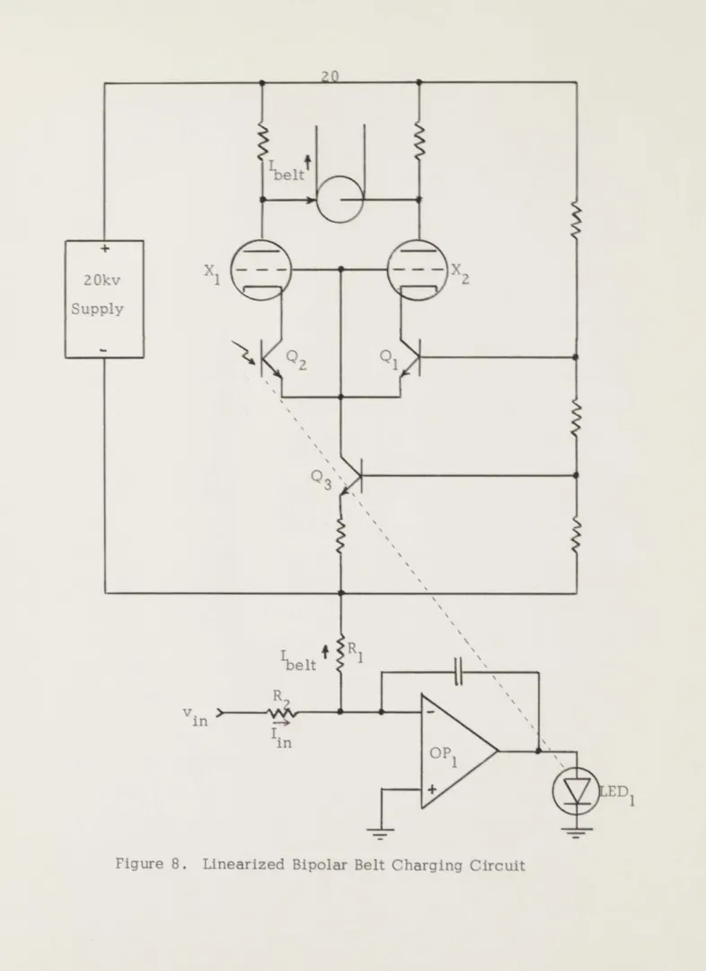
A complete, linearized belt charging circuit based on a high voltage differential output amplifier is shown in Figure 8. Triodes
X and X2, transistor
Q
1, and phototransistorQ2
form a balanceddifferential amplifier in which the state of
Q2
determines the spray voltage and thus the belt current.Q3
is a current source whichsets the bias point of the amplifier. The entire high voltage portion of the circuit is isolated from ground so that any current going onto the belt must appear through R Operational amplifier OP is an
error integrator which provides the very large low frequency gain re-quired for linearization. The feedback loop is closed between OP1
and
Q
via the optical coupler, LED 1. Error detection is performedby the cancellation of belt current Ibelt and input current Vin/R at
the input to OPl.
In order to insure even application of charge to the belt, the charging circuit must be able to detect and correct fluctuation in charging current as rapidly as possible. To this end, it is important that delays occurring in the charging system be kept as short as possible. One area in which a significant delay can occur is at the charging electrodes due to the finite belt speed. A delay in detec-tion of belt current occurs here because belt charge must leave the vicinity of the charging electrodes before it can appear as a current through the resistor, R When charge is applied to the belt beneath the pulley, a delay of more than one quarter of a rotation, or about 5ms, occurs before current is sensed. Measurement delay of this kind can be minimized by making both charging electrodes small or
by otherwise insuring that belt charge spends only a short time near
the charging area. Other delays, which must in general be tolerated, occur due to distributed parasitic capacitance along the large value plate resistors and due to the integrator capacitor.
20kv Supply x1 2 2 Q1
Q
3\"
,belt R in inFigure 8. Linearized Bipolar Belt Charging Circuit
4 4
R
+
21
3.2 Terminal Current Control
It can be seen from the description of the Van de Graaff genera-tor given earlier that the machine's basic operation would not be
significantly altered by charging the belt within the terminal instead of at ground plane. Such a method is called down charge because charge is carried on the down run of the belt.
A primary advantage of down charging is the reduction in delay
between application of charge to the belt and the resulting change in terminal voltage. With up charge systems, charge must be
trans-ported nearly the full length of the column before terminal voltage is significantly affected. In contrast, down charge only needs leave the vicinity of the terminal to cause a terminal voltage change. Other advantages include doubled belt current capacity when both up and down charge are used, and improved belt tensioning.
Passive down charge systems have previously been employed in Van de Graaff generators to improve belt current capacity. In such
systems, up charge current arriving at the terminal creates a
resistive voltage drop which is used to produce the gradient requir-ed for down charging. Because down charge is controlled indirectly
by charge moving into the terminal, the speed of response is not
increased by this method.
A system permitting fast monopolar control of down charge from
the ground plane has been developed at the University of Aarhus, Denmark.2 In this system, a pulse-width modulated signal gener-ated by the control system is optically coupled to terminal locgener-ated charging electronics via a lucite light guide. The terminal elec-tronics decode the optical signal into a high voltage pulse train which performs the belt charging. With this system, no attempt was made to utilize the additional charge capacity of the up run .
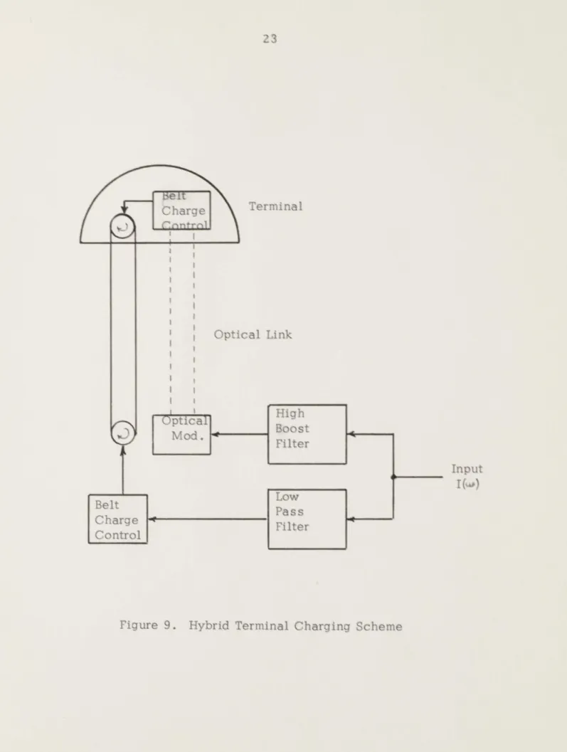
A scheme which attempts to exploit the increased belt charge capacity obtained when up and down charge are used simultaneous-ly, as well as the reduced delay of down charge is shown in
Figure 9. Bipolar belt charging circuits are located in the terminal and at the lower pulley. The terminal located electronics are
controllable by an optical link which permits linear control of down charge from the ground plane. Filters separate the high and low frequency components of the input current signal to insure that fre-quencies at which the up charge delay is significant get channeled only to the down charge system, while at low frequencies up and down charge are about equal. The complete system has a single
input which controls the instantaneous total belt current arriving at the terminal.
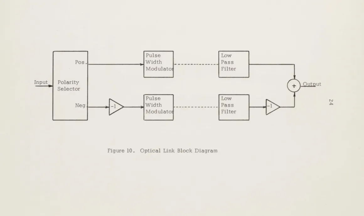
Requirements of the optical link are that the input and output be linearly related and that output be zero when the input is zero. The dual light guide, pulse width modulated system shown in Figure 10
satisfies those requirements. Pulse width modulation is used be-cause linear demodulation can be performed easily by low pass filtration of the modulated signal. The separation of the input sig-nal into positive and negative components insures that for zero in-put there is no optical signal in either guide, and therefore zero output signal. Pulse frequency should be at least ten times faster than the fastest expected charging frequency, or at least 1KHz, to insure that demodulation filtration does not slow generator current response.
Design of separation filters H dn W and H up(w) is simplified by
assuming they each have a single pole at the same frequency and are therefore of the form:
tet tharge Terminal r nntn Optical Link I i I High ptica Boost Mod. Filter Input Low Belt Pass Charge Filter Control
Pos Polarity Selector Neg Pulse Low Width Pass Modulatoi Filter Ut + ut Pulse Low .. Width----.----_-__.-. Pass -l Modulatoi Filter
Figure 10. Optical Link Block Diagram Input
25
Hd
)
Ndn
()Furthermore, lim Hd(w) = lim H
(#)
= 1/2 insures that in the40.4idn
Up
low frequency limit, net terminal current is equally divided be-tween up and down charge. Also, lim H W- (w) = 0 insures that
up
in the high frequency limit, up charge is not utilized; and
lim Hd(w) = 1 insures that the charging system gain is the same
in the low and high frequency limits. These criteria are satisfied by:
Note that Hdn(to) + H up
(W)
= 1 so that, neglecting delay effects, the belt charging scheme has a uniform frequency response.The terminal charging current IT (w) for an input signal I(w) will be given by
I,(>
Rd.)e~"'
H,(I)
P
"
I(W
6
C
Q 1))
where U and ,, are the down and up charge transport delays respectively.
Since T, %,'u , this expression is factorable:
IT(O)
(Hjat)
+ H,,)4
"'P-",,) ,.' " .Note that if the filter design is ineffective, phase cancellation of terminal currents is possible at odd frequency multiples of
to '4 ) for which Hdn(w) and H up(W) can never compensate.
To correct for up charge transit delay, jH up must be signi-ficantly reduced when ew (%-1Q becomes large. The value of
%1 determines how well this is done. Too short a time constant will not suppress phase cancellation of terminal charging currents while too long a time constant results in significant imbalance of belt loading at unnecessarily low frequencies. A good choice for
T1 is the smallest value for which C (w) , the charging transfer function, remains satisfactorily uniform with frequency. A plot of the magnitude of C) = for zero down charge transit delay, for a typical up charge transit time of .08 sec. , and for various filter time constants is shown in Figure 11. In this case, for a value of T. = .40 sec., the ripple in C(w) is less than ldb. Fig-ure 12 is a plot of the minimum value of 1C (w4 as a function of
U 4 -I044 0A
IcotAu
C (6)ClioP c I1N&
ORNE& R
Figu- ---4
Figurell-
1
.;- 1.-.4 .~ __ -IfIJJ
/
. .. . ...\1
* ..-1;
-
-I4
4t 6I I 0/00 .4 '---.4 I. ./044 -... ... . -20A FREQUENCY H*. .100/ 0/ 0 *!to*
.'
0 Noll
M1
k
U~m))l
90
WAIWINIWn
Vo q29 4. VOLTAGE MEASUREMENT
Measurement of terminal voltage in Van de Graaff generators is complicated by their limited current capability and the large voltage to be measured. Resistive dividers of sufficient impedance to pre-vent significant loading of the generator are slowed by distributed capacitances and often become non-linear at high voltages. Capac-itive dividers, on the other hand, are unsatisfactory due to poor low frequency characteristics resulting from capacitor leakage and
measurement circuitry bias current effects. For fast and accurate voltage measurement, more complicated methods are required.
An often used technique, which was described by Trump et.al. in 1940, employs a rotating grounded shutter generating voltmeter
(GVM) to measure the electric field strength due to terminal poten-tial. In these devices, the capacitance which couples a set of
stator plates to the Van de Graaff terminal is modulated by a rotat-ing vane, resultrotat-ing in an AC induction current which flows to the
stator. Rectification of that AC current produces a DC signal which is proportional to the terminal potential.
Because a generating voltmeter is a capacitive device, it can draw no real power from the Van de Graaff generator. Also, because it causes a minimal perturbation of the generator's field, a GVM has very little AC effect on terminal voltage. For these reasons the generating voltmeter is a nearly ideal voltage magnitude measure-ment device.
A GVM can also provide polarity information in the phase
rela-tionship between output current and vane rotation. Appendix Ia shows that the output current from a generating voltmeter has the form:
30
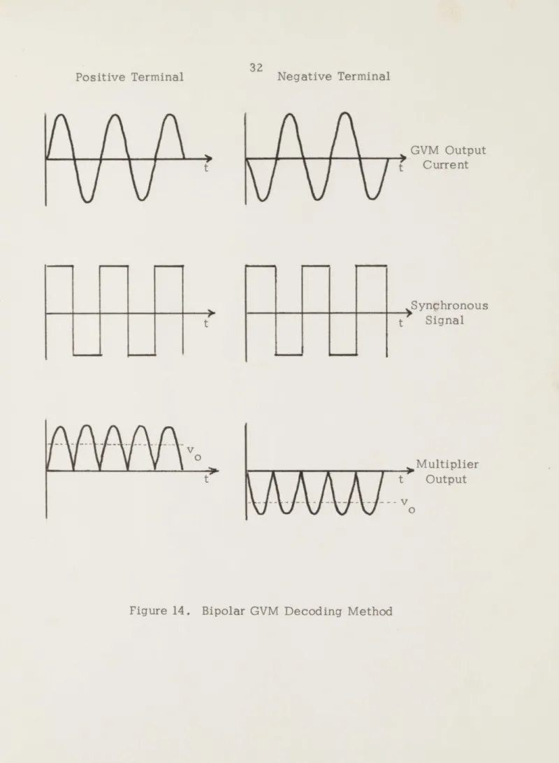
where VT is the Van de Graaff generator terminal voltage and w 0 is the GVM frequency. Note that a change in the sign of terminal voltage has the same effect as a 1800 phase shift at each fre-quency. This suggests that bipolar GVM decoding is possible using synchronous phase detection techniques.
A voltage measurement scheme which takes advantage of the GVM's polarity capability is shown in Figure 13. A sensor at the GVM produces a signal, R(t), synchronous to the vane rotation. A gain stage and clipper reduces R(t) to a square wave R'(t) of known (constant) amplitude and fast rise and fall times. The current out-put from the GVM and R'(t) are then multiplied. As shown in
Figure 14, the resulting signal has an average value which is directly proportional to the terminal potential including sign. A rigorous analysis in Appendix Ib verifies this simple analysis and shows that R'(t) need not be sauare in general, but can be any non-orthogonal signal synchronous to the GVM rotation.
A typical operating frequency for a GVM is 230 Hz. With either full wave rectification or synchronous detection the GVM output is transformed into a signal whose average value represents the ter-minal voltage and which has large components at and above 460 Hz. The low pass filtration which is necessary to remove these compon-ents severely limits the response bandwidth of voltage measurement. As an example, a single pole filter to reduce the 460 Hz components by 40 db rolls off response bandwidth at 5 Hz.
To improve the frequency response of a GVM, it can be combined electronically with a capacitive divider which has good high fre-quency characteristics, but is poor in the DC case. With proper design, such a system could have the good low frequency GVM performance as well as wide bandwidth.
Terminal *GVM Voltage Synchronous Reference Signal Onutnut i (t) Current R (t) SQuaring R' (t) Circuit Low Outpul
(rvYYt
Pass FilterBipolar GVM Decoding Scheme Figure 13.
Positive Terminal
(NA/rV
\JV/
ft v 0 329 Negative TerminalfAf\
KA-
AAA--GVM Output t Current *SynChronous t Signal -,Multiplier t v 0 OutputDetection Plate High Integrator Pass H h Filter Terminal GVMLo Synchronous Flr Detector
Figure 15. Wideband Terminal Voltage Measurement
A detection plate exposed to the Van de Graaff terminal's electric field performs the capacitive voltage measurement. Detection plate current is integrated to produce a signal which is essentially
representative of terminal voltage, and high pass filtered by Hh to eliminate the low frequency components. GVM output is syn-chronous detected and low pass filtered by H (). The two filtered
signals are then summed to produce a wideband representation of terminal voltage.
Filters H1(w) and Hh( ) must: 1) produce outputs whose sum is a
wideband representation of terminal voltage and 2) eliminate syn-chronous frequency components from the GVM and drift components from the detection plate circuitry. For ease of realization H1 (w) and
H h M)are single pole filters of the form:
A
If the GVM output is assumed to be proportional to the terminal volt-age, VT , over the passband of H1 (w) and, similarly, the detection plate current to be proportional to VT over the passband of Hh ' then H (w) and Hh W should satisfy:
Substituting for H1 (w) and Hh(w) and then solving for Hh( ) yields:
The integration and filtration of detection plate current can be com-bined into one filter to form Hh' W:
Note that H h'(w) and H 1 (w) differ only by a gain term.
35
Figure 16. Here GVM and detection plate summation is done before filtration to take advantage of the similar forms of H1 and Hh (). A value of .03 seconds for the filter time constant would suppress synchronous GVM components by 40 db and still be significantly faster than the detection plate leakage time constant.
Detection Plate
GVM Low 1
&Oo Pass jw+a Output
Synchronous Filter
Detector
Figure 16. Alternative Wideband Voltage Measurement Terminal
5. VOLTAGE CORRECTION
5.1 DC Correction
During operation in the DC mode, the function of the
corrector block is to maintain a minimum error between the measur-ed terminal voltage and a reference signal. To help design a
corrector which will optimally perform this function, it is conven-ient to model the entire control system as the servo loop shown in Figure 17. In this model, the corrector subtracts the measured terminal voltage from an input signal to obtain an error signal,
e(w). It then processes e(L) through a filter, H(w), to produce a
charging current.
Design of H(.)) is intimately related to the frequency
characteristics of the other system blocks: M(w), C(w) and G(._). Because the characteristic time constant of a Van de Graaff gener-ator is so long, and because voltage measurement and belt charge control can be made to have comparitively wide bandwidths, it is reasonable to assume that M(-) = M and C G-') = C e over the usable bandwidth of the generator. The form of H(o) is
there-fore primarily determined by the current response, G(w), and the down transit delay.
In his 1969 thesis , Diessner developed a comprehensive lumped element model (Figure 18) from which the Van de Graaff gen-erator frequency response, G(w), can be approximated. To implment this model as a linear system, I assume that the capacitive coupling between belt charge and the equipotential planes is negligible. The model then becomes a recursive RC filter (Figure 19) whose current response can be calculated. Values of the filter elements for a model
Voltage
Measurer-ment M(L)
Filter Charge Terminal
Control Current Terminal
In Cr Response retgeo
H~u>) C(W) G (w)Votg
DC Corrector
Terminal SC R C 1CI R C p
-H
-H
Column Ecuipotential Planes CL
R C C p RC ept ' beltFigure 18. Dynamic Model of a Van de Graaff Generator (from Diessner)
Tank
'belt
t
(delaye T C -I-R IILA A CT
C R C C - I Aiiiiiiiiiiil'll/ f -A -Cl Cl -A--R R C ClVan de Graaff Recursive Filter Model Figure 19.
41
The transfer function of the recursive model has a complex closed form which is difficult to employ in a feedback system analysis. For this reason, it is convenient to use a more approxi-mate, but simpler single pole model in which only terminal capac-itance and column resistance are considered:
IA&CT
Rc and CT are column resistance and terminal capacitance
respective-ly. The similarity of the phase and gain plots of the two models
verifies this approach (Figures 20 and 211). To take into account the small difference between the two models, the single pole equivalent becomes an even better approximation if the terminal capacitance CT
is assumed to be about 20 pf larger than it actually is.
The DC servo loop has now been simplified to that shown in Figure 22. The transfer function for this system is given by:
__
HI _
+
_+IPPC
c,
1
+ ao RcCT And the error is
S vfn- M Vy = '
I~~~~ +
1A~C~
To minimize error, it is desirable to make the denominator of this ex-pression, and therefore H(w), as large as possible. Zero errbr in the
1/
DC case can be insured by including a factor of jw in HW.) so that
H (w) co
The system loop gain and phase shift are:
G,,)
IMC lH&()I/
+Rc~
..
....
....
...
....
....
... .... .... ... Cr x2b0 .. .... .... .... .... . CT XQ >oj CT Noo 10 IT4 444..P
I 1601, "PARM10-4
. .... .... .... .... ... 00 M 0 4 0 0 -... ... u ,n a, 400 - J 0 4 a 0 -T-.--T r .. .... .... .... .... .... .... Ow ... .......
....
....
It. Pole. MO act
IL
IVT(l
Wed
.1you -I-A m FREQVENCY Hi.___ a m 'it 2I~ZI21z14T~Ti2i 2T11F14 w~v.
6'
0 40ri+F12
K'
4
F
V
________IF
4% al 0 J4C f .....
.. .. .. ...
1
...
-j 7 (D. NJ mA a 4 4JIMAL
.---Sitje'PI
dve~oc
#~.
Iii4.
....
...
..
-...-C,-) I0N' i. dO 'ci) J0~ ~1 -t7
80' L-t+LL.44
EL I J- I.- I A .1 1 ... . . .... .... ... ... . .. . 7 t4+1 /071 1.0 10 I cr 14 /d-3 ... . 1-T....
....
...
f4bM
V.FO- H ()- C e e
Figure 22. Simplified DC Control Loop
R c
1 + jwCT R
Terminal Voltage
45
System bandwidth is largely governed by the frequency at which loop phase shift
Q(.o)
approaches 1800. For this reason, a phase lead component in H(o) which compensates for phase lags elsewhere can reduce total loop phase shift and therefore improve useful bandwidth, provided an adequate gain margin can be maintained.A filter of the form
satisfies the zero DC error criterion and also compensates for the phase shift introduced by the very long generator time constant. With a filter of this form, loop gain and phase shift become:
G(W)=
Me
w
Rc
Stability requires that the gain be less than unity when loop phase shift exceeds 1800 ,' when
tAJ 7
Therefore
is required.
Since a large h tends to reduce system error, this inequality is best satisfied by the largest h for which the system stability is satisfactory. Although values for each of the terms in this ex-pression are known fairly well, best performance will be obtained
by adjusting h experimentally.
The correction filter H(M) has been designed assuming that the terminal capacitance CT is fixed. However, CT includes a sig-nificant variable component of up to several hundred picofarads due to the apparatus under test. For this reason, the time constant picked for H (u) must be a compromise which yields good
perform-46
ance for a wide variety of loads. A filter time constant of 5 seconds for the 5MV system has been selected and the resulting loop phase shift with terminal capacitance as an independent parameter is plotted in Figure 23. Note that even for very large capacitance a satisfactory phase margin is maintained.
PU w. 16 L 1 -ra
..
..
....
...
I
L]
41.4
'11W
H
I
H
II
-a'4% 130 I ?d 717: . .,...,...FR~~QV~~N...
v-i
II :...... .... .. 1.0. 4I I Tdp IT-.
14-I/.4 From Measurement Block Input + e (t) H(e) S(1 + JwRcC) To Belt Charge Control
5.2 AC Correction
A pseudo-triangular waveform in which the generator slews at constant belt current magnitude between positive and negative peak voltages is desired in the AC mode. To produce this kind of opera-tion, the AC corrector block must detect when the terminal voltage exceeds an externally controlled threshold level and reverse belt current polarity at that time. A suitable transfer function for the AC corrector block is shown in Figure 259. AC amplitude can be justed by varying the switching threshold level and frequency ad-justed by setting belt current magnitude.
Belt Current Terminal Voltage threshold level
6. CONTROL SYSTEM BLOCK DIAGRAM
A control system block diagram based on the block designs developed in earlier sections is shown in Figure 26. Not shown in this diagram are the sources of the AC and DC reference sig-nals. In normal operation, AC and DC voltage references are manually controlled by front panel potentiometers. For automatic operation, a digitally controlled voltage source permits automatic up-and down-stepping control of terminal voltage. External
control of the generator operation is also permitted by externally providing the necessary reference signals, such as obtainable from commercially available waveform generators.
Detection Plate Page lTver ti Sync GyM AC Input )-High Boost Filr * M PW Modulator
4-Level Detector Off DC DC + * Input DC Correction Filter Low Pass FilterFigure 26. Control System Block Diagram Charge
7. CIRCUITRY DESIGN
The design of circuits which can perform the various control system functions is for the most part straightforward. Designs for each major system block are included here for completeness.
De-signs of the less important blocks (e.g. power supply, voltage references, etc) are not shown due to their triviality.
7.1 Voltage Measurement Circuit
Voltage measurement circuitry is shown in Figure 27. A synchronous signal is obtained from the GVM by allowing vane rota-tion to interrupt a light beam incident on phototransistor PT1. Syn-chronous detection is done by synSyn-chronous chopping of the GVM current waveform by FET1 and FET2 at the input to OP2, rather than by multiplication. This method avoids the drift and linearity pro-blem of an analog multiplier circuit. The GVM signal and detection plate current are summed, filtered, and buffered at OP3.
7.2 DC Loop Corrector
The circuit shown in Figure 28, performs the DC loop correction. The transfer function of this circuit is:
Since the input signals are added rather than subtracted, a positive reference input will produce a negative terminal voltage. A gain control follows this stage to allow trimming of loop gain.
7.3 AC Loop Corrector
Level detection during AC operation is done by the circuit in Figure 29. Operational amplifier OP1 is enclosed by a positive feedback loop and changes state when V = V . OP2 and OP3
in outo the and 0P3
o;Z0 0 W
/V
019 291 /oct ~ ltc f-/je FET) ETI S"IKo 9j-t dec-Ct Ori fpkA+Ec / C
OP3 u--Pp1Tr
(AT
Figure 27. Voltage Measurement Circuit
c-rn CA)
54 10 K PEF IN IC,( y;ELT 4r . DC Loop Corrector Figure 2 8.
Figure 29. AC Level Detector 0 P2 797 <+..3K oOfq 7a Ps 74/o 4.3 .3K ioo Voijt
OP5 normalizes and buffers the output signal, Vout0
7.4 Charge Control
This circuit performs the low pass and high boost decomposi-tion of the charge control input signal and separates the down charge
signal into positive and negative components. OP is a low pass filter for the up charge. OP2 is a high boost filter for the down charge and also performs the polarity decomposition. OP3 inverts the output of OP2 to provide a positive output for the pulse width
modulator.
7.5 Pulse Width Modulator
The pulse width modulator (Figure 31') operates by producing a high output whenever its input is larger than a reference triangular waveform. OP1 and OP2 comprise the trianglar wave generator and
OP3 and OP4 compare the input and reference waveforms. 7.6 Terminal Demodulation Electronics
The terminal located pulse width demodulation electronics are shown in Figure 32. Light incident at photodiode PD1 causes a low output at OP1 and turns on Q2. Photo diode PD2 similarly con-trols the state of Ql. Transistors Q3 and Q4 are current sources, controlled by the states of Q1 and Q2 respectively, which charge the low pass filter at the input to OP2. OP2 is a portion of the belt charging circuit.
7.7 Belt Charging Circuit
The operation of the belt charging circuit has been discussed in detail earlier. A complete circuit diagram with component values is shown in Figure 33. Large 60 hz currents due to capacitive coupl-ing between the secondary windcoupl-ing of the high voltage power supply and its case can interfere with charging circuit operation. This
57
problem is reduced by the addition of capacitor C which is trimmed to cancel AC leakage currents.
2, tou hg opt ~ ~ k9 conlfra cortact RO K 3700K<so 0"' OP2 3
tPu wA"h m&IMator 6RAse fO. Ma.uka.r
Chaos1e I Chamoel
5 9
IKI
1175 1 I -- A
ON1 IIS, Opt
V+
16 gaLEDI t.o&41ht
OftO
pr
INPUT a
1OK t(oK 1I0% I 4s b~elt e6&r~e .,1 LED 10) K I (K v~
Figure 32. Terminal Demodulation Electronics
L
1
ji
goal Mhf ol 5OM SOMFS K
2som110
VAC20 kV
#2k NI TITISI' 1EK Opt + LEb tI(KBelt Charging Circuit Figure 33.
8. SYSTEM PERFORMANCE
Development and testing of the control system was performed using a 2 MV Van de Graaff machine. System operation without down charge was satisfactory up to full voltage in both DC and AC modes. Since the down charge electronics do not fit in the 2 MV terminal, testing with down charge has been postponed until the new facility is completed. Because the new 5 MV generator was not operational, final performance figures could not be obtained. The operation of the measurement circuitry is good. The syn-chronous detector produces a clean bipolar output which shows nearly optimum phasing between the reference and GVM current signals (Figure 34 ). In addition, observed resolution of voltage peaks in the AC mode indicates correct detection plate operation. No attempt has been made to check measurement linearity since space for a linear calibration resistor is not available in the 2 MV machine. Calibration will be performed later during the setup pro-ceedure for the new facility.
Because GVM output current is linearly related to vane speed and because frictional losses which affect speed increase with gas pressure, a measurement error occurs when gas pressure is varied. The frequency of the synchronous signal from the GVM is representa-tive of vane rotation and provides a convenient method of observing this effect. A plot of GVM frequency change as a function of
pressure is shown in Figure 35. This curve suggests that a 3% measurement correction is needed between 0 and 200 psig.
Charging circuit operation is bipolar and linear (Figure 3>) and has a rise time of 10 ms (Figure -37) which suggests a maximum
frequency response of about 30 Hz. A significant amount of noise appears in belt current which is probably due to belt inhomogeneity
Synchronous Signal
Synchronous Detector
Output
Figure 34. Synchronous Detector Output
Charging Current
5 uA/cm
100 As/cm
Figure 37. Charging Circuit Risetime
10 V/cm
.5 v/cR
SPEEDb COMM" GVM SPEED CYANGE6 WIrTh PRESSURE 0 S Figure 35
14 er Se yoao 40% to 0 ftoo 40 voe ' 9 so ttol~ 170 lie s
PRESSURe
CHARGIA/G CIRCUIT V-I PLOT Figure 36 **h4 9m -~A -gJ -md -RA -42-J. L1.1 AV . # .1. 06.J,V, .1, iNmpr VOLTA49 -.I -. 9 -.1t -'l ----4 65 CBRR(T -4u -*A -%4
and incomplete 60 Hz leakage cancellation in the charging circuit. The relatively high frequency of this noise, as well as the other-wise good quality of system performance suggest that it does not
seriously affect terminal voltage. Except for dynamic range limita-tions which occur due to finite power supply vol tage and belt
capacity, charging performance is completely independent of gas pressure and type.
The components of the down charge system have been individ-ually tested and work. In addition, a 36" length of Crofon fiber optics has been exposed to a 2 MV potential difference without
breakdown, suggesting a potentially satisfactory insulation strength. In the AC mode, the control system produces a triangular wave-form which is slightly rounded due to the generator time constant.
(Figure 38) Variations in peak AC voltage are less than 2 kV, and positive and negative charging currents are equal within a micro-ampere.
Control system performance in the DC mode is very good. Ter-minal voltage drift is less than 1 kV and ripple is about 4 kV due mostly to perturbations occurring faster than the up charge re-sponse capability. Using a WAVETEK function generator to provide an input signal, terminal voltage can be made to track .3 Hz
sinusoidal, trapezoidal and triangular waveforms accurately and without significant overshoot. (Figures 39, 40 , 41 , ) By
ad-justing the DC loop gain, overshoot can be optimized as desired (Figure 42). Risetime, however, is high voltage power supply limited and differs for positive and negative polarities due to different charging efficiencies.
At large loop gain settings in the DC mode, the system oscill-ates at about 4 Hz which corresponds to an up charge delay of .06
seconds. Since .08 seconds are required for belt transit, charge within .02 seconds, or one quarter column length of the terminal
appears to influence terminal voltage. This suggests that a down charge delay of at least .02 seconds may be expected.
68 250 kV/cM .25 V/ce Ssec/CR Terminal Voltage System Input Terminal Voltage 250 k/cit sec/cm
Figure 38. AC Mode Terminal Waveform Figure 41. DC Mode Triangular Response
.250 kV/cr Terminal Voltage System Input Termina1 Voltage System Input 1 sec/cA 250 kV/cm .25 V/cx 1 sec/cm
Figure 40. DC Mode Trapezoidal Response Figure 39. DC Mode Sinusoidal Response
Figure 42a. DC Mode Step Respome Terminal voltage Input Terminal Voltage
Figure 42b. DC M)de Step Respoase
Loop gain increases going down.
.0 kV/cm
sec/cm
.25 V/cu
250 ky/cm
9. CONCLUSION
A control system which makes a Van de Graaff generator behave at low frequencies like a voltage amplifier with a gain of 106 has been designed. With this system, it is possible to produce an arbitrary terminal voltage waveform by applying a similar wave-form to an input port. The system's bipolar capability is unique and results from improvements in measurement and belt charging techniques. Good DC stability and the ability to track triangular, trapezoidal and sinusoidal waveforms have been demonstrated
using a 2 MV Van de Graaff machine.
Because of the success of sinusoidal operation, sine waves may replace the triangular shape AC currently employed in testing of compressed gas insulation. Advantages would include ease of analysis, better peak voltage control, reduced column and belt
stress and relevence to practical AC power systems. System improvements could be made in two areas:
1) The fluctuations observed in belt current are disturbing and perhaps could be reduced. This might involve optimization of the design of the spray electrodes or better cancellation of 60 Hz leak-age currents.
2) The variation of GVM calibration with gas pressure is un-desirable. A feedback speed control for the GVM or an electronic correction of voltage measurement would alleviate this problem.
72
APPENDIX Ia
GVM Output Current
Trump has suggested the equivalent circuit shown below for a generating voltmeter used to measure Van de Graaff generator terminal voltage.
VAr
j
Uk)Because of the periodicity of C t(t), it may be written as a Fourier series:
Ct(t-)*
~anCOSnw+
,b.sinnw&where w is the frequency of the GVM output current in radians per
second.
Solving for the short circuit current, i(t):
S
JC,(t)
VT
For slowly varying terminal voltage: Wi) Vr j C
z
Vr w
$b,,ncosnwf -aa cMSin -nwi#%to
(
77 Massachusetts Avenue Cambridge, MA 02139 http://libraries.mit.edu/ask
DISCLAIMER NOTICE
PAGINATION ERROR p.7374
APPENDIX Ib
Synchronous Detection of the GVM Signal
The signal used to extract polarity information from a GVM signal may have any waveshape as long as it is periodic and synchronous to vane rotation. To see this consider the general synchronous signal R (t):
R(6:
rS.,%i
fW+ 4 Qr,, u~s MWoFrom Appendix Ia,
Therefore,
-riW.Afn sinowt Caim't + h C. M aMeieAWt Taking the average value,
a f , aa b
SV1-w
kj~&qfl
r~~The average value of R (t)i (t) is directly proportional to terminal voltage for any synchronous signal R (t). The proportionality
contan, k, is a function of R (t) wave shape, and may be zero for some forms of R(t).
75
APPENDIX II
Calculation of Equivalent Circuit Elements for the 5MV Machine 1. Plane to plane capacitance
Total equipotential plane area: 37.6 in2
Area covered by glass spacer: 19.3 in2
Pitch: 1 in
Relative dielectric constant of the glass: 5.0 Capacitance due to the glass area: 23.3 pf
Area exposed to gas: 18.3 in2
Pitch: 1 in
Relative dielectric constant of gat: 1.00
Capacitance due to exposed area: 4.1 pf
Hoop Area (est.): 7.85 in2
Hoop Separation (est.); .5 in
Capacitance due to hoop: 3.5 pf
Total plane to plane capacitance: Cp = 30.9 pf 2. Plane to tank capacitance
Pitch: 1 in
Column OD: 10 In
Tank ID: 34 5/8 in
Plane to tank capacitance: 4.11 pf
3. Column resistance
Resistor Value: 2 x 10⁹ ohms
Number of Sections: 48
76 BIBLIOGRAPHY
1. Diessner, A.: "Studies in Compressed Gas Insulation"; M.I.T. S.M. Thesis, Elec. Eng. 1969.
2. Miller, G. L., Sorensen, T.: The Stabilization of Van de Graaff Accelerators; Internal Publication, Institute of Physics,
Univer-sity of Aarhus, Denmark, 1972.
3. Trump, J. G., Safford, F. J., Van de Graaff, R. J.: "Generating Voltmeter for Pressure Insulated High Voltage Sources"; Review of Scientific Instruments, 11 (1940).
4. Van de Graaff, R. J., Trump, J. G., Buechner, W. W.: "Electrostatic Generators for the Acceleration of Charged Particles". Reports on Progress in Physics, 11 (1948).
5. Evans, W. W.: Voltage Control of a 3 MEV Van de Graaff Gener-ator; M.I.T. S.M. Thesis, Elec. Eng. 1950.
6. Taft, J. E.: Voltage Stabilizer for an Electrostatic Generator; M.I.T. S.M. Thesis, Elec. Eng. 1950.
7. Walter, A. K.: "Elektrostatische Generatoren"; Akademie-Verlag,