HAL Id: hal-00566657
https://hal-iogs.archives-ouvertes.fr/hal-00566657
Submitted on 4 Apr 2016
HAL is a multi-disciplinary open access
archive for the deposit and dissemination of
sci-entific research documents, whether they are
pub-lished or not. The documents may come from
teaching and research institutions in France or
abroad, or from public or private research centers.
L’archive ouverte pluridisciplinaire HAL, est
destinée au dépôt et à la diffusion de documents
scientifiques de niveau recherche, publiés ou non,
émanant des établissements d’enseignement et de
recherche français ou étrangers, des laboratoires
publics ou privés.
Backscattering in monomode periodic waveguides
Bing Wang, Simon Mazoyer, Jean-Paul Hugonin, Philippe Lalanne
To cite this version:
Bing Wang, Simon Mazoyer, Jean-Paul Hugonin, Philippe Lalanne. Backscattering in monomode
peri-odic waveguides. Physical Review B: Condensed Matter and Materials Physics (1998-2015), American
Physical Society, 2008, 78 (24), pp.245108. �10.1103/PhysRevB.78.245108�. �hal-00566657�
Backscattering in monomode periodic waveguides
B. Wang, S. Mazoyer, J. P. Hugonin, and P. Lalanne*
Laboratoire Charles Fabry de l’Institut d’Optique, CNRS, Univ Paris-Sud, Campus Polytechnique, RD 128, 91127 Palaiseau Cedex, France
共Received 15 April 2008; revised manuscript received 27 September 2008; published 8 December 2008兲
The transport properties of photonic periodic共monomode兲 waveguides in the presence of realistic fabrication errors are analyzed. They are governed by out-of-plane loss and backscattering. We derive a closed-form expression for the mean-free path that characterizes the transition between the ballistic and localization trans-port regimes in these waveguides. In agreement with earlier works, the mean-free path is found to be domi-nantly affected by backscattering for small group velocities. The predictions are quantitatively supported by fully vectorial computational results obtained for two-dimensional periodic waveguides. Three-dimensional 共3D兲 structures, such as single-row-defect photonic-crystal waveguides, have also been analyzed and are shown to provide moderate backscattering in comparison to other 3D waveguides. But in all test cases, we find that the mean-free path is critically small, even for moderately small group velocities of c/50 and for up-to-date fabrication nanofacilities.
DOI:10.1103/PhysRevB.78.245108 PACS number共s兲: 42.70.Qs, 42.25.Fx, 42.79.Gn, 81.16.Nd
I. INTRODUCTION
Planar two-dimensional共2D兲 photonic-crystal 共PhC兲 slabs have attracted much attention recently as a possible platform for densely integrated photonic circuits and different photo-nic functionalities. Engineering the photophoto-nic dispersion rela-tionship might provide unique opportunities for integrated photonics especially in the slow light regime where new compact devices, such as delay lines, optical switches, or Raman lasers, are currently the subject of intense research.1–5
There are many important issues in relation with the use of slow light for optical processing, such as light injection6,7or group-velocity-dispersion-management problems.3,8 A
criti-cal issue is the extrinsic loss that results from inevitable fab-rication errors and that prevent full periodicity to be realized in practice. This implies that even for periodic waveguides operating with a truly guided Bloch mode below the light line of the cladding, light transport is accompanied by out-of-plane and backscattering losses, like in z-invariant waveguides.9–11 There is no motivation for exploring the
slow light regime if any advantage is immediately counter-acted by excessive losses. In this context, several authors12–14
have suggested that the extrinsic losses in periodic waveguides are drastic near the band edge, where the group velocity vanishes, and may even be responsible for light localization.15
In this work, we numerically study the transport of light in monomode periodic waveguides, focusing on the back-scattering loss issue. Through a perturbative first-Born-approximation theory similar to that used in Refs.12,14,16, and17, we derive a universal coefficientthat quantifies the mean-free path induced by backscattering in periodic waveguides 共see Sec. II兲. This coefficient that allows com-parisons of the performance of various waveguides scales as the square of the group index and can be calculated with virtually any Bloch-mode solver. It solely depends on the statistical disorder correlation function and on the slow Bloch-mode field distribution on the scatterers 共Born ap-proximation兲. In Sec. III, we validate the analytical formula
for by comparing the formula predictions with computa-tional results obtained for 2D periodic waveguides with a fully vectorial Fourier modal method.18,19 The comparison
allows us to check the accuracy of the formula and to discuss the transition from the ballistic to the localized trans-port regimes, where multiple scattering becomes predomi-nant. In Sec. IV, we calculate thecoefficient of various 2D and three-dimensional 共3D兲 geometries, such as single-row-defect waveguides in PhC slabs. We find that backscattering is a very critical issue even for small disorders and for op-eration at moderate group velocities. Section V summarizes the work and offers open remarks.
II. BACKSCATTERING ANALYTICAL MODEL
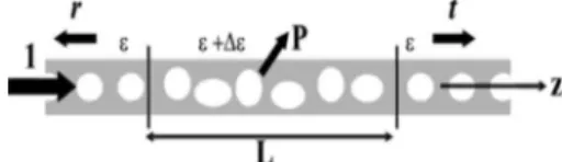
Let us start by considering Fig. 1related to light scatter-ing in a periodic waveguide with imperfections. The unper-turbed waveguide defined by its permittivity and permeabil-ity and=0is assumed to sustain a forward-propagating truly guided Bloch mode denoted by⌽共1兲=兩E共1兲, H共1兲典, being a pseudoperiodic function of the z coordinate, ⌽共1兲共r+az兲 = exp共jk1z兲⌽共1兲共r兲 with Im共k1兲=0; a being the period along
the z direction. As this fundamental mode propagates through the perturbed section, it is backscattered into the backward propagating Bloch mode⌽共−1兲=兩E共−1兲, H共−1兲典 共backscattering loss R兲 and it is radiated in the cladding 共out-of-plane losses
P兲, like in classical z-invariant waveguides.9The scattering
problem defines two quantities r共兩r兩2= R兲 and t 共兩t兩2= T兲 that
correspond to the modal reflection and modal transmission
FIG. 1. Extrinsic loss in a periodic waveguide. The imperfect region 共⌬兲 of length L induces backscattering R=兩r兩2and
coefficients, respectively. We denote by⌬ the dielectric per-turbation in the imperfect section of length L and by ⌽ =兩E,H典: the solution of Maxwell’s equations. In the orthogo-nal Cartesian coordinate共x,y,z兲 system, ⌽ satisfies the curl Maxwell’s equations at a given frequency共/c=2/兲,
⫻ E = j共r兲H, ⫻ H = − j共r兲E − j⌬共r兲E, 共1兲 where j2= −1. Equation共1兲 shows that the imperfections act
as current sources proportional to ⌬ and to the perturbed field. The infinitesimal source −j⌬共r兲E共r兲dr located at r =共x,y,z兲 contributes to the modal Bloch-mode reflection co-efficients by an infinitesimal way. Following the formalism developed in Ref. 20 that relies on the Lorentz reciprocity theorem for periodic waveguides, we have
r = −共/4兲
冕
dr⌬共r兲E共1兲共r兲 • E共r兲, 共2兲where the integral runs over the perturbed region. Note that for Eq. 共2兲 to be valid, the Bloch mode ⌽共1兲has to be nor-malized so that its power flow through any transverse wave-guide cross section is unitary.20 Equation 共2兲 is exact but it
supposes that the scattered field be known in the perturbed region. A fully vectorial calculation of E共r兲 is a challenging task that would require computations in three dimensions with a high resolution in order to capture the small disorder imperfections. However, such computations can be per-formed in two dimensions with a high accuracy and will be used in Secs. III and IV to check the accuracy of the model and its domain of validity.
To keep the treatment at a simple level, we have used a modified first-order Born approximation to derive a semiana-lytical expression for the backscattered intensity in the weak perturbation regime 共ballistic transport兲. The analysis that shares many features with earlier works12,14,16,17is provided in the Appendix for the sake of clarity. In the limit of small disorders and small group velocities, we obtain关see Eq. 共A6兲
in the Appendix兴 具R典 = 共/2兲2共 b−h兲2共/兲2共L/a兲ng2
冕冕
cell ⌫共r1,r2兲 ⫻␣⬘
共r1兲␣⬘
ⴱ共r2兲dr1dr2, 共3兲where the integral runs over the etched surfaces of the unit cell. All quantities are defined in the Appendix. ng is the Bloch-mode group index, is the disorder standard devia-tion,⌫共r1, r2兲 is the normalized displacement statistical cor-relation function, 2⌫共r1, r2兲=具⌬l共r1兲⌬l共r2兲典 with ⌬l共r兲 the local deformation,bandhare the relative permittivities of the etched material and of the etched inclusion, and ␣
⬘
共r兲 = ET共1兲共r兲•ET共1兲共r兲+共bh兲−1DN共1兲共r兲•DN共1兲共r兲, ET共1兲 and DN共1兲 be-ing the normalized tangential electric and normal displace-ment vectors of the Bloch mode⌽共1兲computed at the oper-ating point 共mainly the Brillouin-zone edge in this work兲. Equation共3兲 relies on a number of classical approximations共weak disorder on interfaces only, i.e., no volume disorder, statistical disorder correlation length smaller than the
wave-guide periodicity兲 and allows us to define a dimensionless coefficient = lim →0 具R典 共/兲2共L/兲n g 2, 共4兲 with given by =共/2兲2共b−h兲2共/a兲
冕冕
cell ⌫共r1,r2兲 ⫻␣⬘
共r1兲␣⬘
ⴱ共r2兲dr1dr2. 共5兲Hereafter, we will be concerned by periodic waveguides composed of slits or holes. As a statistical disorder, we con-sider a size disorder model,14,16,17in which the hole radii共or
the slit width兲 are randomly varied around their mean value with a statistical distribution 关see Fig.2共a兲兴. We further
as-sume that distinct etched features 共holes or slits兲 have fully independent deformations关⌫共r1, r2兲=0 if r1and r2are rela-tive to two different holes兴 even within a single unit cell and that the correlation is perfect in the vertical direction. De-pending on the fabrication tool and on the specific wave-guide geometry, the two last hypotheses may be valid or not. However, we believe that they are reasonable for many ge-ometries 共such as single-row-defect PhC waveguides or ridges with slits兲 that are fabricated by electron-beam writing and etching techniques. Thus, the normal local deformation ⌬l共r兲 becomes constant for every etched feature, ⌬l共r兲=⌬l with 具⌬l典=0 and 具⌬l2典=2, and the expression of in Eq.
共5兲 becomes =共/2兲2共b−h兲2共/a兲
兺
i冏
冕
Si ␣⬘
共r兲dr冏
2 , 共6兲which is an incoherent sum over the holes or slits surfaces Si contained in the unit cell. It is important to have in mind that Eq. 共6兲 does not take into account multiple scattering. For
small disorders, this approximation is likely to be valid within a single unit cell; but as photons propagate into the waveguide over long distances, multiple scattering inevitably takes place as we should see in Sec. III.
Equation 共6兲 holds for randomly varying hole radii. This
disorder choice is motivated for its simplicity, especially for comparing our model with fully vectorial calculation results that can only be obtained for simple local deformations. Ac-tually, a more realistic disorder model is shown in Fig.2共b兲, where we introduce the roughness correlation length lc. It is
FIG. 2. Statistical disorder hole model. The local deformation is denoted⌬l共r兲. 共a兲 Simplified size disorder model ⌬l共r兲=⌬l used in this work.共b兲 More realistic model with the roughness correlation length lc. The relationship between the loss predictions obtained with the two models is discussed at the end of Sec. II.
WANG et al. PHYSICAL REVIEW B 78, 245108共2008兲
interesting to briefly identify what is the model predictions for these more realistic deformations; this is straightforward if one assumes that the Bloch-mode field is nearly constant all around the hole circumference. Then the incoherent sum-mation in Eq.共6兲 takes place over the correlation length and
not over the entire circumference 2rh as it is the case for the size disorder model. Consequently, the actualfactor for the realistic model is found to be 2rh/lctimes smaller than that obtained with the simplified model, provided that the same disorder standard deviationis used for the two mod-els. While it is very difficult in practice to estimate accu-rately the roughness disorder even with direct measurements, it is interesting to put realistic numbers. For a W1 PhC wave-guide with hole radius rh⬇120 nm 共see Sec. IV兲 and for a correlation length lc= 70 nm, 2rh/lc⬇9, implying that our simplified model overestimatesby almost an order of mag-nitude. In different words, we could also conclude that the
amount of backscattering that is predicted with the simplified roughness model for a disorder standard deviation
= 1 nm actually corresponds to that predicted with the more
realistic model for = 3 nm. For experiments performed with periodic waveguides with lengths of several millime-ters, it is conceivable that neither the simplified disorder model nor the realistic one strictly applies over the entire waveguide. Then one may consider the model as a tool to infer trends that allow comparing different geometries or technologies rather than as an accurate description providing absolute values.
III. FROM THE BALLISTIC TO THE LOCALIZED TRANSPORT REGIMES
In order to verify the validity and the accuracy of Eqs.共4兲
and 共6兲, we have performed 2D calculations for periodic
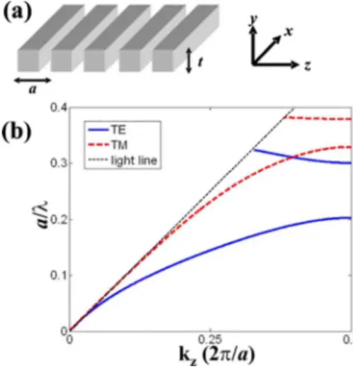
waveguides 共periodicity a=350 nm兲 composed of slits etched in a semiconductor共n=3.5兲 planar slab suspended in air关see Fig.3共a兲兴. As a disorder model, we consider that the slit widths are randomly varied around a mean value 共具w典 = 150 nm兲 according to a Gaussian distribution with stan-dard deviationand that they are all independent. Using the aperiodic-Fourier modal method共a-FMM兲,18,19 we have
cal-culated the Bloch-mode transmittance T =兩t兩2and reflectance R =兩r兩2 of finite-length waveguide sections in the vicinity of the first valence band, wherevgvanishes and where the fun-damental Bloch mode is lossless. The a-FMM, a fully vecto-rial method, is a generalization of Fourier modal methods21
used in grating theories to handle nonperiodic situations by an artificial periodization via the introduction of perfectly matched layers18 or of complex nonlinear coordinate
transformations.19To compute the modal transmission or
re-flection coefficients of the fundamental Bloch mode, we use the Bloch-mode orthogonality and reciprocity relationships.20 For the two-dimensional geometries
consid-ered in that section, a large number of Fourier harmonics共we use 201 harmonics兲 are retained for the computation and high accuracy is achieved. The numerical error bar is within the thickness of the lines used to show the calculated data. The calculations have been performed for the first conduc-tion and valence bands and for both TE 共E field parallel to
the slit兲 and TM 共H field parallel to the slit兲 polarizations 关see Fig.3共b兲for details兴.
The solid lines in Fig.4represent the mean values of the backscattering具R典 averaged over an ensemble of 1000 inde-pendent random disorder realizations, as a function of the normalized length L for various ngandvalues. Figures4共a兲 and4共b兲 are obtained for TE polarization and Figs.4共c兲and
4共d兲hold for TM polarization. All plots correspond to calcu-lation performed for the first valence band. In Figs.4共a兲and
4共c兲,= 1 nm and four values of the group index ng= 25, 50,
FIG. 3. 共Color online兲 2D waveguide geometry considered in this work. 共a兲 Sketched of the geometry composed of air gooves 共width is 150 nm兲 in a semiconductor 共n=3.5兲 slab membrane 共t = 200 nm兲 in air. The period is a=350 nm. Note that the geometry is invariant in the x direction.共b兲 Band diagram of the fundamental guided mode for TE共solid blue兲 and TM 共dashed red兲 polarizations.
FIG. 4. a-FMM calculations 共solid curves兲 and model predic-tions共dashes lines兲 both show a drastic effect of disorder on back-scattering. The results are obtained for the periodic waveguide shown in Fig.3and for the first valence band.共a兲=1 nm for four values of the group index ng= 25, 50, 100, and 200.共b兲 ng= 50 and =1, 2, and 5 nm. 共a兲 and 共b兲 hold for TE polarization. 共c兲 and 共d兲: same as共a兲 and 共b兲 for TM polarization. The a-FMM fully vectorial results for具R典 are obtained for slit-width disorders obeying a nor-mal distribution and are averaged over 1000 independent statistical realizations of disorders.
100, and 200 are considered. Figures 4共b兲 and4共d兲 are ob-tained for ng= 50 and for three values of ,= 1, 2, and 5 nm. For all curves, the average reflectance first scales lin-early with the normalized length before saturating, showing the transition between the ballistic and the diffuse regimes.
The dashed lines represent the linear relationships 具R典 =ng2共/兲2 L/, with the values computed from Eq.共6兲,
= 21 for TE and = 73 for TM. It is noticeable that the dashed lines represent the slope at the origin L = 0 of all the a-FMM data. In our opinion, this represents a strong evi-dence of the validity of Eq. 共6兲, at least for 2D periodic
waveguides, showing that the backscattering loss scales as ng2 共Ref. 12兲 and as 共/兲2 in the ballistic regime 共RⰆ1 and
T⬇1兲, where the Born approximation is valid.
In Fig. 5, we show the averaged out-of-plane scattering losses 具1-R-T典 as a function the normalized length for ng = 50 and for three values of , as in Figs. 4共b兲 and 4共d兲. Again the plots are obtained for the valence bands. The TE polarization case 关Fig. 5共a兲兴 corresponds to a situation for which the out-of-plane losses are much smaller than the backscattering loss. In this regime, 具1-R-T典 scales linearly with L/ and with ng, letting us suspect that one may define a coefficient ␥ 共similar to 兲 for the out-of-plane losses, 具1-R-T典=␥ng共/兲2 L/. Within the Born approximation, the calculation of␥requires that the coupling of the incident guided state ⌽共1兲 with the continuum of radiation states be accurately taken into consideration. Although this calculation can be performed,22,12it is much more intricate than that of
and analytical expressions cannot be obtained. For the TM polarization case关Fig.5共b兲兴, the out-of-plane losses are
sig-nificantly larger than those obtained for TE polarization. The photon transport shows an intricate behavior that combines backscattering and out-of-plane losses. For instance, for = 5 nm, Figs.4共d兲and5共b兲evidence that a saturation regime is obtained for short propagation distances, where ⬇13% of the incident photons are lost in radiation states while the other 87% are backscattered. As shown by other computa-tional data共not shown here for the sake of compactness兲, the relative fractions of photons lost by out-of-plane radiation or by backscattering in the saturation regime depends on ngand
in an intricate way; but the general trend is that as ng increases, backscattering dominates and具R典 tends to 1.22
In all plots, we observe that the averaged backreflection 具R典 and the out-of-plane losses 具1-R-T典 first scale linearly with L in agreement with Eq. 共6兲. For large L values,
mul-tiple scattering occurs and both quantities saturate. This
char-acterizes the transition from ballistic to localization trans-ports, which takes place at typical characteristic lengths equal to the effective mean-free path ᐉ. The latter is im-pacted both by backreflection and by out-of-plane loss and can be defined as the length for which具T典⬇1/2. Neglecting the contribution of out-of-plane scattering ␥ng共/兲2, the mean-free path becomes the length for which具R典⬇1/2, and is approximately given by
ᐉ = 0.5/关ng
2共/兲2兴. 共7兲
Note that this expression neglects the out-of-plane losses and multiple scattering. Thus it only provides an approximate estimation for ᐉ. Actually, this upper bound is found to be fairly small. For instance, for = 1 nm and for a moderate group index of 50, the effective mean-free paths are as small as 30 and 3 for TE and TM polarizations, respectively. The ten-fold variation arises from the electric-field distribu-tion in the slit interfaces. For the first valence band and for TE polarization, the electric field is strongly localized inside the ridges and is thus rather weak on the vertical slit inter-faces. The situation is the opposite for the other polarization because the electric field is dominantly confined in the air slits.
IV. THREE-DIMENSIONAL GEOMETRIES
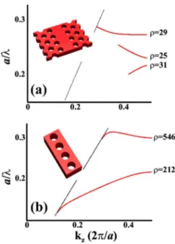
While the numerical results presented so far are obtained for 2D geometries, the model developed in the Appendix can be used to study the effects of disorder-induced backscatter-ing in a variety of waveguide geometries that are essentially one dimensional 共1D兲 in nature. In our opinion, the coeffi-cient that solely depends on the normalized statistical cor-relation function and on the fundamental Bloch mode is an important figure of merit that quantifies the effective mean-free path in periodic waveguides, at least when the radiation losses are smaller than the backscattering losses. Addition-ally,varies as/a, implying that if one scales all the wave-guide parameters with the wavelength, is kept unchanged. Thus the parameter allows for a comparison between vari-ous periodic waveguides. A question arises whether some specific geometries offer lower backscattering losses than others. Especially, one may wonder if the single-row-defect PhC W1 waveguide, which is currently the subject of intense research in the slow light regime,23–26offers low
backscatter-ing losses with respect to other periodic waveguides. To provide a first insight into this question, we have com-puted thefactor of several periodic waveguides for several Bloch modes in the first bands. The results are summarized in Fig.6. Figure6共a兲is related to a classical W1 waveguide in a semiconductor共n=3.5兲 membrane 共thickness 220 nm兲 in air 共hole radius rh= 0.3a and periodicity a = 420 nm兲. As a disorder model, we assume that only the two hole rows sur-rounding the single-row defect are perturbed by a random diameter fluctuation. The W1 waveguide supports three bands. The upper flat one 共with a null group velocity at = 1.55 m兲 corresponds to the classical W1 Bloch mode that lays within the band gap of the photonic crystal and the two other bands at lower energies correspond to index-guided modes. The of the upper band is found to be 29: a value
FIG. 5. Same as in Figs.4共b兲and4共d兲but for the out-of-plane losses具1-R-T典. Note the different scales in 共a兲 and 共b兲. 共a兲: TE. 共b兲: TM.
WANG et al. PHYSICAL REVIEW B 78, 245108共2008兲
comparable to the two other ones. It is important to have in mind that the two lower band frequencies do not correspond to monomode operation since PhC bulk modes also exist at those frequencies. However the first-Born approximation used to derive thefactor remains valid even for multimode waveguides, since Eq. 共2兲 solely relies on the forward and
backward propagating modes ⌽共1兲and⌽共−1兲. Note that Eq. 共2兲 applies to all the guided modes and can be used to
cal-culate backscattering into higher-order modes. However, multimode operation impacts backscattering into the funda-mental mode as shown in Ref.11for z-invariant waveguides; but analyzing this effect requires to go beyond the first-order Born approximation and to consider multiple-scattering situ-ations, for which photons are first scattered into higher-order modes and then backscattered into the fundamental mode. This is beyond the scope of the present work.
We have also performed calculations in two dimensions for the same geometry using an effective index of 2.83 for the refractive index of the semiconductor and a magnetic polarization parallel to the PhC cylinder y axis. The effective index value was chosen so that the cut-off frequency of the
W1 waveguide at the edge of the first Brillouin zone matches
that of the 3D structure. The calculated values are similar to those obtained with the 3D calculations共= 36 instead of 29 for the upper band兲, showing that 2D calculations are quantitatively accurate although they do not take into ac-count the electric-field component that is parallel to the cy-lindrical hole axis.
Figure6共b兲is related to a semiconductor共n=3.5兲 periodic nanowire共width is 500 nm and height is 340 nm兲 in air, with
a hole radius rh= 0.34a. The bands correspond to Bloch modes predominantly TE polarized 共like in the W1兲. The periodicity has been chosen equal to a = 335 nm so that is equal to 1.55 m at the Brillouin-zone edge of the valence band. As for the planar waveguide with slits in TE polariza-tion, we found that thevalue associated to the valence band is significantly smaller than that of the conduction band. The calculation of the values is obtained, as previously, by assuming a hole-diameter disorder model. The value of 212 calculated in the first valence band is significantly larger than that obtained for the W1 waveguide. Similar calcula-tions have been performed for smaller holes共r=50 nm兲, and a significant lowering of the factor for the valence band 共= 5兲 has been obtained. This reduction is also accompanied with a lowering of the band-gap width that becomes compa-rable to that obtained for the W1 waveguide in Fig.6共a兲for the two lower branches.
It is interesting to compare the model prediction for W1 waveguides with experimental results obtained at telecom wavelengths 共=1.55兲. In Ref. 13, transmission measure-ments performed for different lengths 共from 100 m to 1 mm兲 by the cut-back method have shown that for moderate group velocities ng= 40, the total transmission loss are as large as␣= 800 dB/cm. Assuming that the total attenuation is predominantly due to backscattering and that the transmis-sion is given by exp关−ng2共/兲2L/兴 in the localization regime,27we obtain= 1.3 nm by equaling −n
g
2共/兲2L/
and ␣ for = 29 and ng= 40. We regard the value to be physically reasonable, although it is likely to slightly under-estimate the actual disorder standard deviation = 3 – 4 nm, as inferred in Ref. 13 from scanning electron microscopy 共SEM兲 pictures. But we believe that our underestimation of the disorder level basically results from the specific hole size disorder model we use 共see the previous discussion at the end of Sec. II兲. In addition, it is important to realize that the loss measurements in Ref.13are performed in the multiple-scattering 共localized transport兲 regime for propagation lengths much larger than the mean-free path. For this regime, the Born approximation is no longer valid and the intricate interplay between out-of-plane and backscattering losses关see Figs. 4共d兲 and5共b兲, for instance兴 are likely to render our analysis too simplistic. More studies are necessary to under-stand the transport properties in the localization regime.
V. CONCLUSION
Through a perturbative approach, we have derived a uni-versal coefficientthat quantifies the amount of backscatter-ing in periodic waveguides. This coefficient, which solely depends on the statistical disorder model and on the slow Bloch-mode field distribution, can be easily calculated with presently available software. The model predictions have been quantitatively checked 共Fig. 4兲 against fully vectorial
computational results obtained for 2D periodic waveguides composed of slit arrays in slab waveguides. Quantitative agreements have been obtained for all bands and for short propagation distances, showing the validity of the model at least in two dimensions.
The performance of 3D single-row-defect PhC
W1-waveguides has also been analyzed 共Fig.6兲. Due to the
FIG. 6. 共Color online兲 coefficients obtained for 3D periodic waveguide geometries and for various band edges at k =/a. 共a兲
W1 waveguide in a semiconductor 共n=3.5兲 membrane 共thickness
220 nm兲 in air 共rh= 0.3a and a = 420 nm兲. 共b兲 Air-wire semiconduc-tor waveguide 共width is 500 nm; height is 340 nm兲 with rh = 0.34a = 114 nm and a = 335 nm. Similar calculations have been performed for rh= 50 nm and much smaller values for have been obtained 共=5 and 396 for the valence and conduction bands, respectively兲.
side-located periodic holes, the backscattering losses in that waveguide are slightly smaller than those achieved for peri-odic waveguides with similar confinements and with fully centered holes. The gap-guiding mechanism that is a unique property of PhC waveguide does not appear to be crucial in the context of extrinsic losses, at least for small group ve-locities.
In all our simulations, we have found that backscattering due to imperfections is fairly drastic. Although the coeffi-cient of W1 waveguides appears modest in comparison to those of other waveguides, it is found that the mean-free path 关see Eq. 共7兲兴 of these waveguides at telecommunication
wavelengths is only 25 m共60 periods兲: a value that holds for state-of-the-art manufactured waveguides共= 1 nm兲 and for ng= 50. This corresponds to a very small group delay 共 =ᐉng/c兲 of only 5 ps. Thus one may be inclined to operate
W1 waveguides for propagation lengths that are larger than
the effective mean-free path, as it is often the case in experi-mental situations.13,26 Backscattering losses共as well as
out-of-plane diffraction that has not been considered here兲 may then become prohibitive. But more importantly for signal processing, one should expect a drastic pulse broadening be-yond the ballistic regime: in the localized regime, the es-sence of the energy transport is multiple scattering and the transmitted light experiences many backward and forward reflections as it propagates.
ACKNOWLEDGMENTS
This research is partly supported under the European con-tract SPLASH of the 6th EU Framework program and by the Agence Nationale de la Recherche under contract MIRA-MAN of the French ANR Nano2006. We acknowledge fruit-ful discussions with C. Sauvan, L. C. Andreani, and J. J. Greffet.
APPENDIX
In this appendix, we develop a modified Born approxima-tion to derive a semianalytical expression for the backscat-tered intensity in the weak perturbation regime. Figure1 is related to light scattering in a periodic waveguide with im-perfections. The waveguide is formed by air holes in a semi-conductor background. Within a given section of length L, the waveguide is assumed to be perturbed by fabrication er-rors. Figure7shows an example of an exaggerated perturba-tion, where a circular air 共h= 1兲 hole in the semiconductor 共b= 3.5兲 background is deformed. The local deformation de-fined on the hole interfaces at position r is denoted by⌬l共r兲. The deformation defines two different regions with positive ⌬ 共⌬l⬎0兲 and negative ⌬ 共⌬l⬍0兲. With up-to-date nano-fabrication facilities, roughness and disorder are in the nan-ometer range, while typical Bloch confinements are of the order of the wavelength. Thus, with a good approximation, the perturbed regions can be all considered as infinitely small surfaces and by assuming that the electromagnetic fields are locally constant within the deformation thickness 共static limit兲, the volume integral over the perturbed regions in Eq. 共2兲 can be replaced by a surface integral over all the hole
interfaces contained in the perturbed section of length L
r = −共/4兲共b−h兲
冕
dr⌬l共r兲E共1兲共r兲 • E共r兲, 共A1兲 where E共1兲共r兲 and E共r兲 are defined on the interface.Referring to Eq.共A1兲, the first-order Born approximation
merely consists in replacing the unknown perturbed electric field E共r兲 by the fundamental Bloch-mode 共unperturbed兲 field E共1兲共r兲. However, this replacement has to be handled with caution. At a position r corresponding to a positive⌬l, the unknown perturbed field E共r兲 is well approximated by the unperturbed Bloch-mode electric field E共1兲共r兲 calculated on the outer boundary of the hole; a quantity that we further denote by E共1,out兲. Similarly, for r in a region with ⌬l⬍0, E共r兲 is approximated by the fundamental Bloch-mode field E共1,in兲calculated on the inner boundary of the hole. In both cases,⌬l⬎0 or ⌬l⬍0, the product E共1兲共r兲•E共r兲 in Eq. 共A1兲
is equal to E共1,in兲共r兲•E共1,out兲共r兲. The relevancy of this non-standard replacement is easily understood if one considers that the unknown field E共r兲 is approximately given by the fundamental Bloch mode of every perturbed cell. As we have checked with fully vectorial computational results for the backscattering R of perturbed waveguides in two dimen-sions, this replacement that leads to a nonstandard Born ap-proximation increases the numerical accuracy of the model predictions.17
Thus for tangential electric-field components that are con-tinuous across the surfaces, E共1,out兲共r兲=E共1,in兲共r兲=ET共1兲共r兲 and
E共r兲•E共1兲共r兲 is simply given by E共1兲共r兲•E共1兲共r兲. For normal electric-field components that are discontinuous across the interfaces, bE共1,out兲共r兲=hE共1,in兲共r兲=DN共1兲共r兲; DN共1兲 being the displacement vector of the fundamental Bloch mode. E共r兲•E共1兲共r兲 then reduces to 共bh兲−1DN共1兲共r兲•DN共1兲共r兲. To summarize, within the limit of small perturbation regions, the modified Born approximation results in
r = −共/4兲共b−h兲
冕
dr⌬l共r兲␣共r兲, 共A2兲 where the integral runs over the dielectric interfaces共e.g., the unperturbed hole boundaries兲 and the complex number␣ is given byFIG. 7. Modified first-order Born approximation leading to Eq. 共A2兲. The three main quantities ⌬l共r兲, E共1兲共r兲, and E共r兲 in Eq. 共A1兲
are all defined for the regions with positive and negative⌬.
WANG et al. PHYSICAL REVIEW B 78, 245108共2008兲
␣共r兲 = ET共1兲共r兲 • ET共1兲共r兲 + 共bh兲−1DN共1兲共r兲 • DN共1兲共r兲. 共A3兲 In Eq. 共A3兲, ET共1兲 共respectively, DN共1兲兲 refers to the tangential 共respectively, normal兲 components of the Bloch-mode elec-tric 共respectively, displacement兲 fields. Note that a related tensor description of roughness has been used in Refs. 14
and17.
The mean reflectance 具R典 of the perturbed section of length L is then easily derived from Eq.共A2兲, and assuming
that ⌬l is null on ensemble average, one gets 具R典 = 共/4兲2共
b−h兲22
冕冕
⌫共r1,r2兲␣共r1兲␣ⴱ共r2兲dr1dr2, 共A4兲 where each integral runs over the perturbed interfaces. In Eq. 共A4兲, ⌫共r1, r2兲 represents the normalized displacementcor-relation function defined by2⌫共r1, r2兲=具⌬l共r1兲⌬l共r2兲典, with
具 典 a notation for ensemble averages. Hereafter, we assume that the disorder displacements induced by the fabrication errors are independent from one unit cell to the other共in the main text, we will further assume that the ⌬l’s of distinct holes within a single cell are also independent兲. Within this reasonable hypothesis共see main text兲, Eq. 共A4兲 becomes
具R典 = 共c/2兲2共b−h兲2共/兲2共L/a兲
冕冕
cell
⌫共r1,r2兲 ⫻␣共r1兲␣ⴱ共r2兲dr1dr2, 共A5兲
with a being the waveguide period. The contribution of ev-ery cell adds incoherently on average and the mean back-scattering scales linearly with the waveguide-section length
L. Equation共A5兲 that neglects multiple-scattering processes
provides a semianalytical expression for the averaged back-scattering. The latter solely depends on the Bloch mode of the unperturbed waveguide through␣共r兲 and on the displace-ment correlation function of the statistical disorder through ⌫共r1, r2兲 defined within one cell.
Equation共A5兲 applies to any Bloch mode at any point in
the dispersion diagram共, kz兲. To analytically explicit the vg dependence of具R典, we must consider a Bloch mode with a small group velocityvgin the vicinity of an operating point wherevg vanishes, for instance, at the Brillouin-zone edge. Let us define by E共1兲and H共1兲 the Bloch-mode electric and magnetic fields at vg= 0 normalized such that 兰cell共兩E共1兲兩2
+兩H共1兲兩2兲dr=4a. Because any Bloch mode with a unitary transverse power flow satisfies 兰cell共兩E共1兲兩2+兩H共1兲兩2兲dr
= 4a/vg共Ref.20兲, ET共1兲or DN共1兲in Eq.共A3兲 can approximately be written as ET共1兲=共vg兲−1/2ET共1兲or DN共1兲=共vg兲−1/2DN共1兲, showing that the Bloch-mode electric and magnetic fields scale as 共vg兲−1/2. Therefore, in the limit of small disorders and small
vg’s, we obtain 具R典 = 共/2兲2共 b−h兲2共/兲2共L/a兲ng 2
冕冕
cell ⌫共r1,r2兲 ⫻␣⬘
共r1兲␣⬘
ⴱ共r2兲dr1dr 2, 共A6兲where␣
⬘
共r兲=ET共1兲共r兲•ET共1兲共r兲+共bh兲−1DN共1兲共r兲•DN共1兲共r兲 is de-fined for the scaled fields calculated at the operating point in the dispersion diagram, essentially the Brillouin-zone edge in this work. Note that the last approximation leading to Eq. 共A6兲 is not strictly necessary for our analysis and that Eq.共A5兲 is more accurate for large vgvalues. However, Eq.共A6兲 that requires only a single Bloch-mode calculation at some operating point of interest allows explicitly emphasizing the group-velocity impact on the backscattered intensity.
*Corresponding author; [email protected]
1M. Soljacic and J. D. Joannopoulos, Nature Mater. 3, 211
共2004兲.
2T. F. Krauss, Phys. World 19共2兲, 32 共2006兲. 3D. Mori and T. Baba, Opt. Express 13, 9398共2005兲.
4Y. A. Vlasov, M. O’Boyle, H. F. Hamann, and S. J. McNab,
Nature共London兲 438, 65 共2005兲.
5M. L. Povinelli, S. Johnson, and J. Joannopoulos, Opt. Express
13, 7145共2005兲.
6Y. A. Vlasov and S. J. McNab, Opt. Lett. 31, 50共2006兲. 7P. Velha, J. P. Hugonin, and P. Lalanne, Opt. Express 15, 6102
共2007兲.
8A. Yu. Petrov and M. Eich, Appl. Phys. Lett. 85, 4866共2004兲. 9D. Marcuse, Bell Syst. Tech. J. 48, 3187共1969兲.
10A. Garcia-Martin, J. J. Saentz, and M. Nieto-Vesperinas, Phys.
Rev. Lett. 84, 3578共2000兲.
11S. A. Bulgakov and M. Nieto-Vesperinas, J. Opt. Soc. Am. A 15,
503共1998兲.
12S. Hughes, L. Ramunno, J. F. Young, and J. E. Sipe, Phys. Rev.
Lett. 94, 033903共2005兲.
13E. Kuramochi, M. Notomi, S. Hughes, A. Shinya, T. Watanabe,
and L. Ramunno, Phys. Rev. B 72, 161318共R兲 共2005兲.
14L. C. Andreani and D. Gerace, Phys. Status Solidi B 244, 3528
共2007兲.
15S. Mookherjea, J. S. Park, S.-H. Yang, and P. R. Bandaru, Nat.
Photonics 2, 90共2008兲.
16D. Gerace and L. C. Andreani, Opt. Lett. 29, 1897共2004兲. 17S. G. Johnson, M. L. Povinelli, M. Soljacic, A. Karalis, S.
Ja-cobs, and J. D. Joannopoulos, Appl. Phys. B: Lasers Opt. 81, 283共2005兲.
18E. Silberstein, P. Lalanne, J. P. Hugonin, and Q. Cao, J. Opt. Soc.
Am. A 18, 2865共2001兲.
19J. P. Hugonin and P. Lalanne, J. Opt. Soc. Am. A 22, 1844
共2005兲.
20G. Lecamp, J. P. Hugonin, and P. Lalanne, Opt. Express 15,
11042共2007兲.
21See, for instance, M. G. Moharam, E. B. Grann, D. A. Pommet,
and T. K. Gaylord, J. Opt. Soc. Am. A 12, 1068共1995兲.
22G. Lecamp, P. Lalanne, and J. P. Hugonin, Phys. Rev. Lett. 99,
023902共2007兲.
23L. H. Frandsen, A. V. Lavrinenko, J. Fage-Pedersen, and P. I.
24D. Mori, S. Kubo, H. Sasaki, and T. Baba, Opt. Express 15,
5264共2007兲.
25N. Ozaki, Y. Kitagawa, Y. Takata, N. Ikeda, Y. Watanabe, A.
Mizutani, Y. Sugimoto, and K. Asakawa, Opt. Express 15, 7974 共2007兲.
26L. O’Faolain, T. P. White, D. O’Brien, X. D. Yuan, M. D. Settle,
and T. F. Krauss, Opt. Express 15, 13129共2007兲.
27On ensemble averages, the transmission in the localization
re-gime decays exponentially when the system size is much larger than the localization length共Refs.10and11兲. This condition is
likely to be fulfilled in the experiments performed in Ref. 13
since the PhC-waveguide lengths are in the millimeter range.
WANG et al. PHYSICAL REVIEW B 78, 245108共2008兲