HAL Id: hal-02899117
https://hal.archives-ouvertes.fr/hal-02899117
Submitted on 14 Jul 2020HAL is a multi-disciplinary open access archive for the deposit and dissemination of sci-entific research documents, whether they are pub-lished or not. The documents may come from teaching and research institutions in France or abroad, or from public or private research centers.
L’archive ouverte pluridisciplinaire HAL, est destinée au dépôt et à la diffusion de documents scientifiques de niveau recherche, publiés ou non, émanant des établissements d’enseignement et de recherche français ou étrangers, des laboratoires publics ou privés.
Electroluminescence from HgTe Nanocrystals and its
Use for Active Imaging
Junling Qu, Prachi Rastogi, Charlie Gréboval, Delphine Lagarde, Audrey
Chu, Corentin Dabard, Adrien Khalili, Hervé Cruguel, Cédric Robert, Xiang
Xu, et al.
To cite this version:
Junling Qu, Prachi Rastogi, Charlie Gréboval, Delphine Lagarde, Audrey Chu, et al.. Electrolumi-nescence from HgTe Nanocrystals and its Use for Active Imaging. Nano Letters, American Chemical Society, 2020, �10.1021/acs.nanolett.0c02557�. �hal-02899117�
Electroluminescence from HgTe Nanocrystals and its Use for Active Imaging
Junling Qu1, Prachi Rastogi1, Charlie Gréboval1, Delphine Lagarde2, Audrey Chu1, Corentin
Dabard1, Adrien Khalili1, Hervé Cruguel1, Cédric Robert2, Xiang Zhen Xu3, Sandrine Ithurria3,
Mathieu G. Silly4, Simon Ferré5, Xavier Marie2, Emmanuel Lhuillier1*
1 Sorbonne Université, CNRS, Institut des NanoSciences de Paris, INSP, F-75005 Paris, France. 2Université de Toulouse, INSA-CNRS-UPS, LPCNO, Toulouse, France.
3 Laboratoire de Physique et d’Etude des Matériaux, ESPCI-Paris, PSL Research University,
Sorbonne Université Univ Paris 06, CNRS UMR 8213, 10 rue Vauquelin 75005 Paris, France.
4 Synchrotron-SOLEIL, Saint-Aubin, BP48, F91192 Gif sur Yvette Cedex, France.
5New Imaging Technologies SA, 1 impasse de la Noisette 91370 Verrières le Buisson, France.
Abstract: Mercury telluride (HgTe) nanocrystals are among of the most versatile infrared (IR) materials with the absorption of first optical absorption which can be tuned from visible to the THz range. Therefore, they have been extensively considered as near IR emitters and as absorbers for low-cost IR detectors. However, the electroluminescence of HgTe remains poorly investigated in spite of its ability to go toward longer wavelengths compared to traditional lead sulfide (PbS). Here, we demonstrate a light emitting diode (LED) based on an indium tin oxide (ITO)/zinc oxide (ZnO)/ZnO-HgTe/PbS/gold stacked structure, where the emitting layer consists of a ZnO/HgTe bulk heterojunction which drives the charge balance in the system. This LED has low turn-on voltage, long lifetime, and high brightness. Finally, we conduct short wavelength infrared (SWIR) active imaging, where illumination is obtained from a HgTe NC-based LED, and demonstrate moisture detection.
Keywords: narrow band gap nanocrystals, HgTe, electroluminescence, active imaging, short wave infrared.
Nanocrystals (NCs) are promising building blocks for optoelectronic devices.1 Their first mass
market application is their use as green and red down-converters for displays.2,3 Their narrow
photoluminescence (PL) compared with scintillators, such as Ce:YAG used previously, enables wider gamut displays. The next step is to switch the display light source from optical down converter-based devices to electrically operated ones4,5 (i.e. light emitting diodes: LEDs) to reduce power
consumption and also to enhance image contrast. When it comes to infrared (IR) wavelengths,6
most of the work has been focused on NC absorption to build devices such as solar cells7–9 and IR sensors10,11 rather than NC emission. However, there is also a demand for IR emitting devices
especially in active IR imaging applications. Currently, in the near and short-wave IR (NIR and SWIR), most of the sources rely on epitaxially-grown quantum well structures made of III-V semiconductors. Such sources have been highly desirable for telecommunication where high emitted power and fast modulation are mandatory requirements. Epitaxial structures suffer though, from a restricted spectral tunability, in a range of wavelengths where organic emitters are ineffective. Thus, NCs may offer an alternative that enables spectral tunability.
In the NIR and SWIR, lead sulfide (PbS)12 is the most investigated material under NCs form.
However, PbS suffers from a long PL lifetime13 (µs and more), which prevents high brightness. In
addition, in lead chalcogenides, the states in the vicinity of the Fermi level are highly degenerated (8 times) and thus, achieving population inversion for stimulated emission appears relatively challenging. Because of these limitations, other NIR materials including InAs14, silver
chalcogenides,15–18 CIGS19,20 and derivatives, as well as mercury chalcogenides have been recently
investigated.21 Particularly, II-VI semiconductors benefit from a higher growth maturity among this
class of compounds22,23 including the growth of 2D emitters called nanoplatelets with narrow
emission linewidth.24 HgTe NCs are certainly the most mature candidates among them. Its vicinity
with the bulk HgCdTe alloy has attracted years of efforts to grow confined forms of HgTe for light emission,25–31 including stimulated emission.32 Paradoxically, researches on electrical pumping of
HgTe NCs are still at an early stage.33,34
In the SWIR, the contrast in an image comes, as in the visible, from an external light source scattered differently on the objects/surfaces of the scene. This differs with the mid-IR where thermal contrast is enabled (i.e. contrast results from the blackbody radiation). Active imaging with an external IR light source is used for SWIR sensing. Briefly, active imaging is a mode of imaging where an invisible light source illuminates a scene from which scattered photons get collected by a focal plane array. Beyond obvious defense and surveillance applications, such active imaging is widely used for industrial vision. Typical applications include moisture detection and material sorting. In this paper, we develop a high brightness LED based on HgTe NCs, and demonstrate its use as IR light source for relevant active imaging applications.
We first grow colloidal HgTe NCs which will be used as a SWIR emitters. The procedure follows one proposed by Geiregat et al.32 Basically, mercury salts react with Te precursors in the presence of
thiols and a coordinating solvent (oleylamine) at low temperature (≈60 °C). The obtained NCs have small sizes of around 4 nm, according to transmission electron microscopy (TEM, Figure 1b) and X-ray diffraction pattern (Figure S1). The optical feature appears in the SWIR with an absorption edge at 1100 nm (1.12 eV) and Stoke shifted PL presents a maximum at 1300 nm (0.95 eV), see Figure 1a and S2-3. The PL quantum yield in solution has been determined to be 45 ±5 %. The time-resolved PL intensity is characterized by a main decay time of about 20 ns (Figure 1c), which is in agreement with recent measurements of the radiative recombination of the HgTe NCs confined states25. This PL decay time is two orders of magnitude shorter than the one measured for PbS
NCs35. It is also noteworthy that longer decay times (≈400 ns) can be evidenced in Figure 1c at the
end of the kinetic. This can be attributed to recombinations involving localized states at the surface of the NCs32.
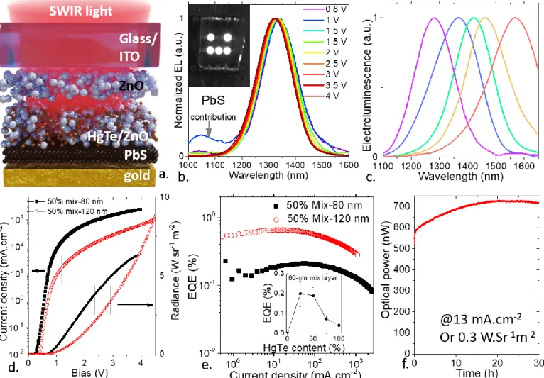
Figure 1a. Absorption and photoluminescence spectra of HgTe NCs. b. TEM image of HgTe NCs showing PL emission at 1300 nm. c Photoluminescence intensity as a function of time after excitation with 1.5 ps laser pulses at 780 nm for a film of HgTe NCs (100%) and mixtures of HgTe and ZnO NCs (25-75 % in volume ratio).
In a typical NC-based LED structure, the emissive NC layer is sandwiched by charge transport layers (CTLs), whose roles are to promote the electrons or the holes injected from contact electrodes to NC conduction or valence bands respectively, to radiatively recombine with each other. As a result, the design of a LED depends on the identification of CTLs with appropriate energy levels and conduction properties. For a LED working in IR range, the increase of the energy difference between the electron and hole transport layers is far less an issue due to the reduced energy spacing between conduction and valence bands of the emitters.
In the IR range, LEDs and laser diodes based on III-V epitaxially-grown semiconductors are made of a p-n junction at which interface a quantum well is introduced to facilitate the exciton recombination. A colloidal equivalent of this design has been proposed by Pradhan et al.36 The n-
and p-sides of the junction rely respectively on well-established layers of ZnO and EDT-capped PbS NCs, which are commonly utilized for solar cells.37,38 The recombination layer is constituted of a
mixture of ZnO and PbS NCs. Here, we apply this concept to the electroluminescence from HgTe NCs. The design of the LED is depicted in Figure 2a, Figure 3a and S22-23. The ZnO electron injection/hole blocking layer (see Figure S6-8) and PbS with an EDT capping (see Figure S9-11) used as hole injector are vertically surrounding an emitting layer consisting of a mixture of HgTe and ZnO NCs (see Figure S4-5 and S15-S21).
In this HgTe/ZnO mixture, the integrity of each particle is preserved, and the absorption spectrum is the sum of the two materials (Figure S14) while a limited shift of the photoemission core level is
observed (Figure S21). Also, the PL dynamics of the pristine HgTe are preserved, see Figure 1c. On the other hand, mixing two materials provides an interesting platform to tune the doping level and conduction properties of the emitting layer.
Photoemission spectroscopy is used to probe the valence band of the HgTe/ZnO layer, see Figure 2b. As HgTe NCs are introduced to the ZnO film, we observe new states in the vicinity of the Fermi level which gradually shifts the valence band toward the Fermi level, making the material more p-type, see the inset of Figure 2b. This observation is consistent with the p-type nature of pristine HgTe (Figure S4), whose introduction to the n-type ZnO (Figure S7) gives rise to an intermediate situation. This hypothesis is further confirmed by transport measurements conducted in an electrolyte-gated field effect transistor configuration,39 see the inset of Figure 2c. A ZnO-based
device shows a typical n-type conduction40 with a rise of conduction under electron injection (i.e.
positive gate bias), see Figure 2c. Whereas, HgTe NCs only device presents an opposite behavior with p-type conduction, see Figure 2e, consistent with the photoemission data indicating the Fermi level in the vicinity of the valence band (Figure 2b and S4).
As a mixture of HgTe and ZnO is prepared (see TEM in Figure S22), we obtain an ambipolar conduction with both electron and hole conductions, see Figure 2d. Using energy dispersive X-ray spectroscopy (EDX, see Figure S13 and Table S1), the optimal ratio of HgTe to ZnO for highest LED performance (25-50 % in volume ratio) is estimated to be ≈ 1 HgTe per ZnO NC. Such ratio is compatible with the formation of percolation paths for each type of carrier forming a bulk heterojunction.
Figure 2a. Energy band profile for a diode made of ITO/ZnO/HgTe/PbS/Au. b. Low binding energy part of the photoemission spectra, relative to the valence band, for samples of ZnO/HgTe with various HgTe content. The inset provides the change in the relative position of the valence band with respect to the Fermi level as a function of the HgTe content in a ZnO/HgTe mixture. c. Transfer
curves (i.e. drain and source current as a function of gate bias) of ZnO NCs. The drain source bias is set at 1 V. The inset is a scheme of the electrolyte gated transistor. ZnO displays only n-type conduction. d. Transfer curves of a 50:50 ZnO/HgTe NCs mixture. The drain source bias is set at 500 mV. The mixture presents an ambipolar behavior. e. Transfer curves of HgTe NCs. The drain source bias is set at 500 mV. HgTe displays only p-type conduction.
In the following, we fabricate the ITO/ZnO/HgTe-ZnO/PbS/Au diode, see a scheme of the device in Figure 3a. When a forward bias is applied, we observe a clear electroluminescence (EL) signal, see Figure 3b, its inset, and S25. The energy of this signal matches well the HgTe PL peak, see Figure 1a. It is also worth noting that the EL energy can easily be tuned by changing the size of the particles from 1250 to 1600 nm, overlapping with the whole telecom range, see Figure 3c.
The turn-on voltage of the EL is ≈0.6 V, see Figure 3d, which reveals a clear sub band gap (0.95 eV for these HgTe NCs) operation. Also note that replacement of the PbS NCs by other conventional MoO3 hole injector has led to significantly reduce performance (EQE around 10-3 % and increased
turn on voltage (0.85 V). Interestingly, there is a small contribution of the PbS NCs layer in the EL at 1050 nm under operating biases just above the turn-on voltage, see Figure 3b. The latter disappears under bias > 1 V, because of the less favorable electron injection within the PbS layer when higher bias is applied.
We also note a small blue-shift of the EL signal as higher bias is applied. Stark effect is expected to reduce the band gap of the material under electric field, which should red-shift the EL spectrum,41
contrary to our observation. This difference might be a result of heating. For HgTe, the band gap increases with temperature, see Figure S2 with a dEG/dT of 68 µeV.K-1. As current flows, Joule
effect may lead to a rise of the junction temperature. Here, we observe a 16 meV shift between the turn on voltage and 4 V operation. To obtain such a shift from heating, the temperature should rise by ≈235 °C, which will have undoubtedly damaged the HgTe NCs that are grown at around 60 °C. Actually, the effect of heating should be explained by the generalized Kirchoff’s law42,43 in which the
non-equilibrium of the carrier leads to such a blue-shift.
The maximum external quantum efficiency (EQE) is 0.67% (Figure 3e) and appears to be strongly dependent with the ZnO content (inset of Figure 3e). To determine the optimal ratio of the mixture, a series of devices based on emitting layer of identical thicknesses (80 nm) are compared. As shown in the inset of Figure 3e and figure S26, the maximum EQE increases strongly with the addition of ZnO to the HgTe, and the optimal ratio is between 25% and 50% of HgTe, which corresponds to ≈1:1 HgTe to ZnO NC ratio. As the emissive layer is switched from pure HgTe to a blend of HgTe and ZnO, we observe an increase of the PL magnitude, the PL signal is multiplied by a factor 1.8 as the HgTe content is the blend is reduced from 100 % to 25 %, indicating that ZnO plays a role in the HgTe NCs surface passivation. However, this enhancement of the PL is weaker than the one observed for the LED EQE, suggesting thatbthe main role of the ZnO is connected to transport. Incorporating ZnO not only allows the formation of the bulk heterojunction as previously discussed (ambipolar transport), but also reinforces the hole blocking behavior in the emitting part of the device, optimizing the charge balance. The thickness dependence of the emitting layer is further tested, based on the 50:50 HgTe/ZnO, and the best performance comes from a device with a 120 nm HgTe/ZnO emitting layer, see Figure 3e and f. Interestingly, under a 500 mA.cm-2 current density,
we obtain a radiance of 9 W.Sr-1m-2, which is similar to the value reported for PbS LEDs with a 10
times higher EQE.36 This high brightness is enabled by the fact that the onset of EQE droop
(J1/2EQE≈0.75 A.cm-2, the current density at which EQE drops by half) is much higher than for LEDs
Auger recombination in HgTe.44 It is also worth pointing that the proposed device significantly
enhances the performance (EQE is tens of times higher, turn on voltage is reduced by half) of previously reported LED based on HgTe NCs, see Table S2.33,34 Last, we have tested the operating
lifetime of the diode (see Figure 3f) and observe a quasi-constant performance over a 30 h period at a high radiance of 0.32 W.Sr-1.m-2.
Figure 3a. Scheme of a diode made of ITO/ZnO/ZnO-HgTe/PbS/Au emitting SWIR light. b. Normalized electroluminescence spectra of the diode depicted in part a and operated under different bias. The inset shows five operating diodes imaged with a SWIR camera (InGaAs detector). c. Normalized electroluminescence spectra obtained from various HgTe NCs in the diode depicted in part a. d. Current and radiance as a function of applied bias for two thicknesses of the emitting layer and with a 50:50 volume ratio of HgTe and ZnO solution. e. EQE as a function of the applied current for two thicknesses of the emitting layer and with a 50:50 volume ratio of HgTe and ZnO solution. The inset provided shows the EQE as a function of the HgTe content in the emitting layer. f. Optical power as a function of time for a diode operated under constant current condition (13 mA.cm-2) corresponding to an initial irradiance of 0.32 W. Sr-1.m-2.
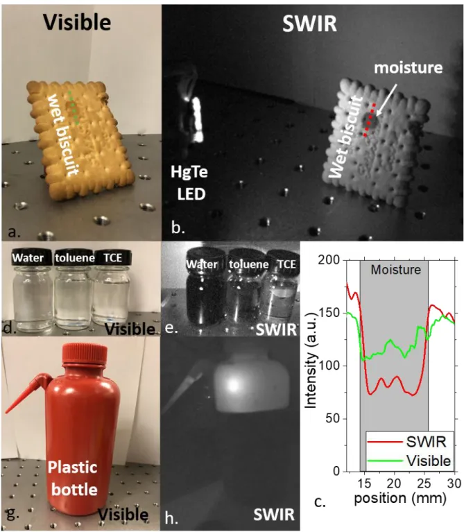
In the last part, we utilize the high brightness of the LED to test its potential for SWIR active imaging. The HgTe NCs based LED is used as a light source while an InGaAs focal plane array (WiDy SenS camera from NIT) is used to collect the scattered light from the scene. The logarithmic operation allows to image scene with large contrast (i.e. the direct signal of the LED and the scattered light from the scene) without saturation.
A typical application of SWIR imaging relates to water detection. While water is transparent in the visible, it strongly absorbs in the SWIR. It is then possible to segregate it from other chemicals transparent in the visible range, see Figure 4d and e. This property is also used to control ripening and detect moisture in food production lines. Here, we show the ability to detect moisture stain on a
wet biscuit, see Figure 4a and b. SWIR imaging increases the contrast along the moisture stain by a factor of ≈3 compared to the visible image, as shown in Figure 4c. SWIR imaging can also be used to see through certain plastic materials. In Figure 4g and h, we image in the visible and in the SWIR (also see video S1) a PET bottle filled with water. In the visible, the plastic is opaque, and it is impossible to observe the content of the bottle, while in the SWIR, we clearly observe the presence of absorbing liquid. Similarly, SWIR imaging can easily distinguish coffee solution from PbS NCs (Figure S27 and video S2 where the bright solution is PbS, while the dark solution is coffee), while in the visible they present a similar brown color.
Figure 4 Visible (a) and SWIR (b) image of a biscuit presenting a moisture stain. c. Modulation of the intensity of the scattered light from the biscuit around the moisture stain. In the SWIR, the contrast is ≈3 times higher. Visible (d) and SWIR (e) image of vials containing various solvent (water, toluene, tetrachroloethylene : TCE). Visible (g) and SWIR (h) image of a PET washing bottle with water in it. For all SWIR images, only the HgTe LED is used as light source (i.e. no visible light contribution).
To summarize, we have demonstrated a SWIR LED based on HgTe NCs. The diode is based on ITO/ZnO/HgTe-ZnO/PbS/gold stacked structure. The emitting layer consists of a ZnO/HgTe mixture which enables the formation of a bulk heterojunction with ambipolar conduction and allows to tune the hole injection within the emitted layer, and its optimal ratio is around ≈1 HgTe per ZnO NC. This diode being based only on inorganic layers rises great promises to also address longer wavelengths in the future. The LED achieves sub-band gap turn on voltage (< 0.6 V), long operating time (>30 h) and broad spectral tunability from 1250 to 1600 nm. Even though the EQE remains modest (0.67%), the diode achieves high brightness (9 W.Sr-1.m-2) at relatively low current density due to a high onset
of EQE droop. This brightness is then used to conduct SWIR active imaging, leading to clear moisture detection with enhanced contrast. Our finding paves the way for an all nanocrystal based active imaging setup by combining the proposed LED with the recent demonstration of HgTe nanocrystal based SWIR focal plane array.45
ASSOCIATED CONTENT Supporting Information
The Supporting Information is available free of charge on the ACS Publications website at DOI: Details are given about Nano material fabrication (HgTe, ZnO and PbS nanocrystals), Material characterization (Structural characterization, Spectroscopic characterization, Photoelectron spectroscopy, Transport measurements, Investigation of the HgTe/ZnO mixture), LED fabrication and characterization and Comparison with state of the art and finally active imaging.
Video S1: SWIR imaging though a PET bottle revealing the presence of water inside also see Figure 4g-h.
Video S2 SWIR imaging of two solutions (PbS QD in toluene and coffee) with brownish aspect in the visible.
COMPETING INTEREST
The authors declare no competing financial interest.
ACKNOWLEDEGMENTS
The project is supported by ERC starting grant blackQD (grant n° 756225) and Ne2Dem (grant n° 853049). We acknowledge the use of clean-room facilities from the “Centrale de Proximité Paris-Centre”. This work has been supported by the Region Ile-de-France in the framework of DIM Nano-K (grant dopQD). This work was supported by French state funds managed by the ANR within the Investissements d'Avenir programme under reference ANR-11-IDEX-0004-02, and more specifically within the framework of the Cluster of Excellence MATISSE and also by the grant IPER-Nano2, Copin (ANR-19-CE24-0022), Frontal (ANR-19-CE09-0017), Graskop (ANR-19-CE09-0026). JQ
thanks Chinese Scholarship Council for PhD funding while AC thanks Agence innovation defense.
REFERENCES
(1) Konstantatos, G.; Sargent, E. H. Colloidal Quantum Dot Optoelectronics and Photovoltaics; Cambridge University Press, Cambridge, 2013.
(2) Bourzac, K. Quantum Dots Go on Display. Nature News 2013, 493, 283.
(3) Jang, E.; Jun, S.; Jang, H.; Lim, J.; Kim, B.; Kim, Y. White-Light-Emitting Diodes with Quantum Dot Color Converters for Display Backlights. Advanced Materials 2010, 22, 3076–3080.
(4) Dai, X.; Zhang, Z.; Jin, Y.; Niu, Y.; Cao, H.; Liang, X.; Chen, L.; Wang, J.; Peng, X. Solution-Processed, High-Performance Light-Emitting Diodes Based on Quantum Dots. Nature 2014,
515, 96–99.
(5) Wood, V.; Bulović, V. Colloidal Quantum Dot Light-Emitting Devices. Nano Reviews 2010, 1, 5202.
(6) Lu, H.; Carroll, G. M.; Neale, N. R.; Beard, M. C. Infrared Quantum Dots: Progress, Challenges, and Opportunities. ACS Nano 2019, 13, 939–953.
(7) Semonin, O. E.; Luther, J. M.; Choi, S.; Chen, H.-Y.; Gao, J.; Nozik, A. J.; Beard, M. C. Peak External Photocurrent Quantum Efficiency Exceeding 100% via MEG in a Quantum Dot Solar Cell. Science 2011, 334, 1530–1533.
(8) Luther, J. M.; Law, M.; Beard, M. C.; Song, Q.; Reese, M. O.; Ellingson, R. J.; Nozik, A. J. Schottky Solar Cells Based on Colloidal Nanocrystal Films. Nano Lett. 2008, 8, 3488–3492. (9) McDonald, S. A.; Konstantatos, G.; Zhang, S.; Cyr, P. W.; Klem, E. J. D.; Levina, L.; Sargent,
E. H. Solution-Processed PbS Quantum Dot Infrared Photodetectors and Photovoltaics.
Nature Materials 2005, 4, 138–142.
(10) Lhuillier, E.; Guyot-Sionnest, P. Recent Progresses in Mid Infrared Nanocrystal Optoelectronics. IEEE Journal of Selected Topics in Quantum Electronics 2017, 23, 1–8. (11) Hafiz, S. B.; Scimeca, M.; Sahu, A.; Ko, D.-K. Colloidal Quantum Dots for Thermal Infrared
Sensing and Imaging. Nano Convergence 2019, 6, 7.
(12) Hines, M. A.; Scholes, G. D. Colloidal PbS Nanocrystals with Size-Tunable near-Infrared Emission: Observation of Post-Synthesis Self-Narrowing of the Particle Size Distribution. Adv.
Mater. 2003, 15, 1844–1849.
(13) Liu, H.; Guyot-Sionnest, P. Photoluminescence Lifetime of Lead Selenide Colloidal Quantum Dots. J. Phys. Chem. C 2010, 114, 14860–14863.
(14) Tessler, N.; Medvedev, V.; Kazes, M.; Kan, S.; Banin, U. Efficient Near-Infrared Polymer Nanocrystal Light-Emitting Diodes. Science 2002, 295, 1506–1508.
(15) Vasilopoulou, M.; Kim, H. P.; Kim, B. S.; Papadakis, M.; Ximim Gavim, A. E.; Macedo, A. G.; Jose da Silva, W.; Schneider, F. K.; Mat Teridi, M. A.; Coutsolelos, A. G.; et al. Efficient Colloidal Quantum Dot Light-Emitting Diodes Operating in the Second near-Infrared Biological Window. Nature Photonics 2020, 14, 50–56.
(16) Qu, J.; Goubet, N.; Livache, C.; Martinez, B.; Amelot, D.; Gréboval, C.; Chu, A.; Ramade, J.; Cruguel, H.; Ithurria, S.; et al. Intraband Mid-Infrared Transitions in Ag2Se Nanocrystals: Potential and Limitations for Hg-Free Low-Cost Photodetection. J. Phys. Chem. C 2018, 122, 18161–18167.
(17) Sahu, A.; Qi, L.; Kang, M. S.; Deng, D.; Norris, D. J. Facile Synthesis of Silver Chalcogenide (Ag2E; E = Se, S, Te) Semiconductor Nanocrystals. J. Am. Chem. Soc. 2011, 133, 6509–
6512.
(18) Yarema, M.; Pichler, S.; Sytnyk, M.; Seyrkammer, R.; Lechner, R. T.; Fritz-Popovski, G.; Jarzab, D.; Szendrei, K.; Resel, R.; Korovyanko, O.; et al. Infrared Emitting and Photoconducting Colloidal Silver Chalcogenide Nanocrystal Quantum Dots from a Silylamide-Promoted Synthesis. ACS Nano 2011, 5, 3758–3765.
(19) Cassette, E.; Pons, T.; Bouet, C.; Helle, M.; Bezdetnaya, L.; Marchal, F.; Dubertret, B. Synthesis and Characterization of Near-Infrared Cu−In−Se/ZnS Core/Shell Quantum Dots for In Vivo Imaging. Chem. Mater. 2010, 22, 6117–6124.
(20) Panthani, M. G.; Akhavan, V.; Goodfellow, B.; Schmidtke, J. P.; Dunn, L.; Dodabalapur, A.; Barbara, P. F.; Korgel, B. A. Synthesis of CuInS2, CuInSe2, and Cu(InxGa1-x)Se2 (CIGS)
Nanocrystal “Inks” for Printable Photovoltaics. J. Am. Chem. Soc. 2008, 130, 16770–16777. (21) Green, M.; Mirzai, H. Synthetic Routes to Mercury Chalcogenide Quantum Dots. J. Mater.
Chem. C 2018, 6, 5097–5112.
(22) Goubet, N.; Thomas, M.; Gréboval, C.; Chu, A.; Qu, J.; Rastogi, P.; Chee, S.-S.; Goyal, M.; Zhang, Y.; Xu, X. Z.; et al. Near- to Long-Wave-Infrared Mercury Chalcogenide Nanocrystals from Liquid Mercury. J. Phys. Chem. C 2020, 124, 8423-8430.
(23) Keuleyan, S.; Lhuillier, E.; Guyot-Sionnest, P. Synthesis of Colloidal HgTe Quantum Dots for Narrow Mid-IR Emission and Detection. J. Am. Chem. Soc. 2011, 133, 16422–16424.
(24) Izquierdo, E.; Robin, A.; Keuleyan, S.; Lequeux, N.; Lhuillier, E.; Ithurria, S. Strongly Confined HgTe 2D Nanoplatelets as Narrow Near-Infrared Emitters. J. Am. Chem. Soc. 2016, 138, 10496–10501.
(25) Sergeev, A. A.; Pavlov, D. V.; Kuchmizhak, A. A.; Lapine, M. V.; Yiu, W. K.; Dong, Y.; Ke, N.; Juodkazis, S.; Zhao, N.; Kershaw, S. V.; et al. Tailoring Spontaneous Infrared Emission of HgTe Quantum Dots with Laser-Printed Plasmonic Arrays. Light: Science & Applications 2020, 9, 1–10.
(26) Keuleyan, S.; Kohler, J.; Guyot-Sionnest, P. Photoluminescence of Mid-Infrared HgTe Colloidal Quantum Dots. J. Phys. Chem. C 2014, 118, 2749–2753.
(27) Rogach, A.; Kershaw, S. V.; Burt, M.; Harrison, M. T.; Kornowski, A.; Eychmüller, A.; Weller, H. Colloidally Prepared HgTe Nanocrystals with Strong Room-Temperature Infrared Luminescence. Advanced Materials 1999, 11, 552–555.
(28) Harrison, M. T.; Kershaw, S. V.; Burt, M. G.; Eychmüller, A.; Weller, H.; Rogach, A. L. Wet Chemical Synthesis and Spectroscopic Study of CdHgTe Nanocrystals with Strong Near-Infrared Luminescence. Materials Science and Engineering: B 2000, 69–70, 355–360.
(29) Rogach, A. L.; Koktysh, D. S.; Harrison, M.; Kotov, N. A. Layer-by-Layer Assembled Films of HgTe Nanocrystals with Strong Infrared Emission. Chem. Mater. 2000, 12, 1526–1528. (30) Harrison, M. T.; Kershaw, S. V.; Rogach, A. L.; Kornowski, A.; Eychmüller, A.; Weller, H. Wet
Chemical Synthesis of Highly Luminescent HgTe/CdS Core/Shell Nanocrystals. Advanced
Materials 2000, 12, 123–125.
(31) Kalytchuk, S.; Adam, M.; Tomanec, O.; Zbořil, R.; Gaponik, N.; Rogach, A. L. Sodium Chloride Protected CdHgTe Quantum Dot Based Solid-State Near-Infrared Luminophore for Light-Emitting Devices and Luminescence Thermometry. ACS Photonics 2017, 4, 1459–1465. (32) Geiregat, P.; Houtepen, A. J.; Sagar, L. K.; Infante, I.; Zapata, F.; Grigel, V.; Allan, G.; Delerue,
C.; Van Thourhout, D.; Hens, Z. Continuous-Wave Infrared Optical Gain and Amplified Spontaneous Emission at Ultralow Threshold by Colloidal HgTe Quantum Dots. Nature
Materials 2018, 17, 35–42.
(33) Koktysh, D. S.; Gaponik, N.; Reufer, M.; Crewett, J.; Scherf, U.; Eychmüller, A.; Lupton, J. M.; Rogach, A. L.; Feldmann, J. Near-Infrared Electroluminescence from HgTe Nanocrystals.
ChemPhysChem 2004, 5, 1435–1438.
(34) O’Connor, É.; O’Riordan, A.; Doyle, H.; Moynihan, S.; Cuddihy, A.; Redmond, G. Near-Infrared Electroluminescent Devices Based on Colloidal HgTe Quantum Dot Arrays. Applied
Physics Letters 2005, 86, 201114.
(35) Clark, S. W.; Harbold, J. M.; Wise, F. W. Resonant Energy Transfer in PbS Quantum Dots. J.
Phys. Chem. C 2007, 111, 7302–7305.
(36) Pradhan, S.; Di Stasio, F.; Bi, Y.; Gupta, S.; Christodoulou, S.; Stavrinadis, A.; Konstantatos, G. High-Efficiency Colloidal Quantum Dot Infrared Light-Emitting Diodes via Engineering at the Supra-Nanocrystalline Level. Nature Nanotechnology 2019, 14, 72–79.
(37) Chuang, C.-H. M.; Brown, P. R.; Bulović, V.; Bawendi, M. G. Improved Performance and Stability in Quantum Dot Solar Cells through Band Alignment Engineering. Nature Materials 2014, 13, 796–801.
(38) Lu, K.; Wang, Y.; Liu, Z.; Han, L.; Shi, G.; Fang, H.; Chen, J.; Ye, X.; Chen, S.; Yang, F.; et al. High-Efficiency PbS Quantum-Dot Solar Cells with Greatly Simplified Fabrication Processing via “Solvent-Curing.” Advanced Materials 2018, 30, 1707572.
(39) Lhuillier, E.; Ithurria, S.; Descamps-Mandine, A.; Douillard, T.; Castaing, R.; Xu, X. Z.; Taberna, P.-L.; Simon, P.; Aubin, H.; Dubertret, B. Investigating the N- and p-Type Electrolytic Charging of Colloidal Nanoplatelets. J. Phys. Chem. C 2015, 119, 21795–21799.
(40) Roest, A. L.; Kelly, J. J.; Vanmaekelbergh, D.; Meulenkamp, E. A. Staircase in the Electron Mobility of a ZnO Quantum Dot Assembly Due to Shell Filling. Phys. Rev. Lett. 2002, 89, 036801.
(41) Rosencher, E.; Vinter, B. Optoélectronique: cours et exercices corrigés; Dunod: Paris, 2002. (42) Wang, H.; Aassime, A.; Le Roux, X.; Schilder, N. J.; Greffet, J.-J.; Degiron, A. Revisiting the
Role of Metallic Antennas to Control Light Emission by Lead Salt Nanocrystal Assemblies.
(43) Greffet, J.-J.; Bouchon, P.; Brucoli, G.; Marquier, F. Light Emission by Nonequilibrium Bodies: Local Kirchhoff Law. Phys. Rev. X 2018, 8, 021008.
(44) Melnychuk, C.; Guyot-Sionnest, P. Slow Auger Relaxation in HgTe Colloidal Quantum Dots.
J. Phys. Chem. Lett. 2018, 9, 2208–2211.
(45) Chu, A.; Martinez, B.; Ferré, S.; Noguier, V.; Gréboval, C.; Livache, C.; Qu, J.; Prado, Y.; Casaretto, N.; Goubet, N.; et al. HgTe Nanocrystals for SWIR Detection and Their Integration up to the Focal Plane Array. ACS Appl. Mater. Interfaces 2019, 11, 33116–33123.