HAL Id: hal-01834228
https://hal.archives-ouvertes.fr/hal-01834228
Submitted on 13 Jul 2018
HAL is a multi-disciplinary open access archive for the deposit and dissemination of sci-entific research documents, whether they are pub-lished or not. The documents may come from teaching and research institutions in France or abroad, or from public or private research centers.
L’archive ouverte pluridisciplinaire HAL, est destinée au dépôt et à la diffusion de documents scientifiques de niveau recherche, publiés ou non, émanant des établissements d’enseignement et de recherche français ou étrangers, des laboratoires publics ou privés.
Multilevel Thermally Assisted Magnetoresistive
Random-Access Memory Based on Exchange-Biased
Vortex Configurations
C. Levartoski de Araujo, S. Alves, Liliana Buda-Prejbeanu, Bernard Dieny
To cite this version:
C. Levartoski de Araujo, S. Alves, Liliana Buda-Prejbeanu, Bernard Dieny. Multilevel Thermally As-sisted Magnetoresistive Random-Access Memory Based on Exchange-Biased Vortex Configurations. Physical Review Applied, American Physical Society, 2016, 6 (2), pp.024015. �10.1103/PhysRevAp-plied.6.024015�. �hal-01834228�
Multilevel thermally assisted magnetoresistive random access
memory based on exchange–biased vortex configurations
C. I. L. de Araujo1,2,3,4, S. G. Alves4, L. D. Buda-Prejbeanu1,2,3,4 and B. Dieny1,2,3,4
1Univ. Grenoble Alpes, INAC-SPINTEC, F-38000 Grenoble, France 2CEA, INAC-SPINTEC, F-38000 Grenoble, France
3CNRS, SPINTEC, F-38000 Grenoble, France
4Laboratory of Spintronics and Nanomagnetism (LabSpiN), Universidade Federal de
Viçosa, Viçosa-MG, 36570-900, Brazil
Abstract
A new concept of multilevel thermally assisted MRAM is proposed and investigated by micromagnetic simulations. The storage cells are magnetic tunnel junctions in which the storage layer is exchange biased and in vortex configuration. The reference layer is an unpinned soft magnetic layer. The stored information is encoded via the position of the vortex core in the storage layer. This position can be varied along two degrees of freedom: radius and in-plane angle. The information is read out from the amplitude and phase of the tunnel magnetoresistance signal obtained by applying a rotating field on the cell without heating the cell. Various configurations are compared in which the soft reference layer consists of either a simple ferromagnetic layer or a synthetic antiferromagnetic sandwich (SAF). Among those, the most practical is one with SAF reference layer in which the magnetostatic interaction between SAF and storage layer was minimized. This type of cells should allow to store at least 40 different states per cell representing more than 5 bits per cell.
Introduction
Since the discovery of tunnel magnetoresistance (TMR) at room temperature in magnetic tunnel junctions (MTJ) [1,2], magnetoresistive random access memory (MRAM) technologies have been extensively investigated. In the last few years, MRAMs have been identified with resistive RAM as one of the most promising technology of non-volatile memories allowing downsize scalability to and beyond the 16nm technology node. Thanks to their very large endurance, they are even envisioned as a possible replacement of DRAM. Indeed, the DRAM technology becomes increasingly complex as the feature size keeps on decreasing below 20nm. MRAMs gather a number of advantages since they are non-volatile, exhibit good downsize scalability, quasi-infinite endurance and invulnerability against ionizing radiations in hard environment applications, like aerospace or nuclear technology. Furthermore, they are compatible with CMOS technology by integrating magnetic tunnel junctions (MTJ) between metallic levels of CMOS technology [3].
In MRAM devices, the storage element within each bit cell is an MTJ, which comprise two ferromagnetic layers, denominated storage and reference layers, separated by a thin insulating layer acting as a tunnel barrier. In in-plane magnetized MTJ, the reference layer magnetization is usually pinned by coupling with an adjacent antiferromagnetic layer (exchange bias phenomenon), while the storage layer magnetization can be switched upon writing. Most of the previously developed MRAM are for binary storage. Their two logic states (“0” and “1”) correspond to two possible orientations of the storage layer magnetization. The in-plane anisotropy yielding these two stable magnetization orientations is usually a uniaxial magnetic shape anisotropy obtained by giving to the cell and elongated elliptical shape. Each MTJ is connected in series with a selection transistor. Upon reading, the transistor is turned on so that a current can flow through the MTJ. The cell magnetic state is then assessed from the MTJ resistance value, high or low corresponding to a “1” or a “0” logical state, thanks to the MTJ TMR. The MRAM technologies are divided in several generations, which differ by their writing process. The first to stand out was the field written toggle MRAM, using a synthetic antiferromagnetic (SyAF) sandwich in the storage layer [4]. The elliptical bit cell is located between orthogonal writing lines (bit and word lines) with long axis oriented at 45o with respect to them. To toggle the magnetization of the
storage layer, a sequence of pulses of current is applied in the orthogonal writing lines, which cross each other at the addressed memory point. These pulses of current create local magnetic fields on the storage layer magnetization in order to switch it in the desired direction. This sequence of write pulses is such that the net field acting on the storage layer magnetization rotates by 3 successive steps of 45°. This applied field first induces a scissoring of the SyAF storage layer magnetization creating a net moment, which then rotates with the rotating field in three steps of approximately 45°. When the field is switched off, the SyAF storage layer relaxes to its antiferromagnetic configuration along the easy axis resulting in-fine in a 180° rotation of its magnetization [5]. Toggle MRAM technology provides good bit selectivity, but presents a poor downsize scalability due to the large current (~10mA) required to create the magnetic field pulses and to the associated electromigration limit in the field generating lines [5].
To lower the memory power consumption and the requirement for large writing field of toggle MRAM, a thermally assisted writing approach was proposed (TA-MRAM) [6]. This approach allows circumventing the classical dilemma in storage technology between the stability of the written information (retention) and the memory writability [7]. The approach consists in temporarily heating the memory element upon write so as to reduce the energy barrier separating the two memory states. Once heated, the storage layer magnetization is switched with a low field (~5mT). After magnetization switching, the cell cools back to its standby temperature where the energy barrier recovers its large value. This approach has been mostly implemented with in-plane magnetized storage layer. In this case, the storage layer is advantageously coupled to an antiferromagnetic (AF) layer [7]. Thanks to the phenomenon of exchange bias, the storage layer magnetization is pinned by the adjacent AF layer up to the AF blocking temperature. Above this temperature, the storage layer magnetization is no longer pinned and can be easily switched by an applied field. Since the storage layer magnetization is here pinned by the adjacent AF layer, there is no need to give to the cell an elliptical shape. Consequently, in TA-MRAM, the cells can be circular. The AF coupled to the storage layer is chosen with a blocking temperature lower than the AF pinning the reference layer (typically 200°C versus 350°C) so that upon heating at about 220°C, the storage layer magnetization can be switched whereas the reference layer magnetization always remains in the same state. During the writing process, the transistor is turned on to generate a current through the MTJ, thus heating the storage layer up to the AF blocking temperature. Thanks to the circular shape of the bit cells
and correlative absence of shape anisotropy, only a weak magnetic field of a few mT is then sufficient to switch the storage layer magnetization [8]. The TA-MRAM power consumption can be further reduced by sharing the field pulse between all bits of a given word [8]. This however remains a field-written technology and therefore has also a limited downsize scalability albeit better than that of toggle MRAM thanks to the lower write field and field sharing.
However, nowadays, the mainstream MRAM technology is based on spin transfer torque writing (STT-MRAM), a phenomenon independently predicted by Slonczewski and Berger [9][10], not requiring any field line. When the transistor is turned on, an applied current flows through the MTJ. This current becomes spin-polarized when traversing the reference layer. The spin-spin-polarized electrons then tunnel through the tunnel barrier and, due to their exchange interactions with those responsible for the local magnetization, exert a torque on the storage layer magnetization [9]. If the current is large enough, the storage layer magnetization then switches parallel or antiparallel to the reference layer magnetization depending on the current direction through the stack (upwards or downwards). STT induced switching in MTJ was first observed in 2004 [11]. STT-MRAM offers much better downsize scalability then field-written MRAM, especially STT-MRAM based on out-of-plane magnetized MTJs [3]. However, the fact that at each write event, the tunnel barrier is exposed to a significant voltage pulse (~0.5V) can cause reliability and endurance issues [12][13]. This becomes more critical if one tries to increase the switching speed to address for instance SRAM type of applications. Indeed, the faster the switching, the larger the voltage pulse has to be, especially below typically 5ns write pulse [3]. To circumvent this problem, another write approach based on spin orbit torque (SOT) switching was recently proposed [14-18]. This approach seems promising for high speed operation. However, due to the larger footprint associated with the 3-terminal geometry, it does not allow high density.
In all the generations described above, the memories have only two states per bit. These MRAM are intended for binary storage. A multilevel concept of STT-MRAM consisting in stacking several MTJs was proposed but the implementation in real products looks extremely challenging due to very narrow margins and reduced performances in terms of write and read speed [19].
A multilevel storage approach in TA-MRAM was also proposed based on the possibility, thanks to the use of an exchange biased storage layer, to set the storage
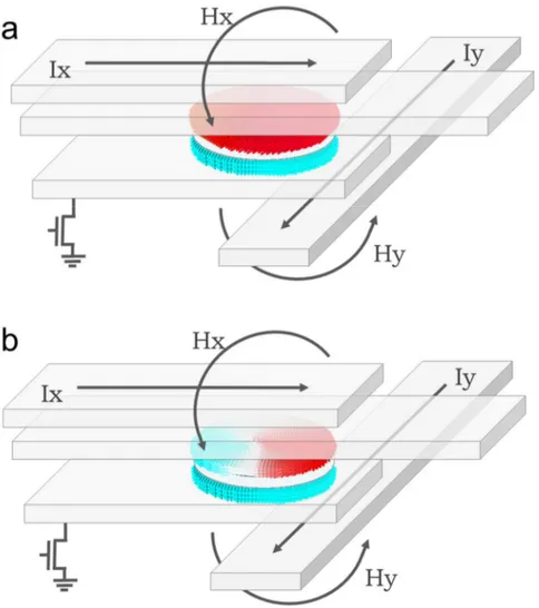
layer magnetization not only in two opposite directions along an easy-axis but in any in-plane direction. Multilevel storage can then be achieved by applying the write field in one of a number of predetermined in-plane directions, as presented in Figure 1a, thanks to two sets of orthogonal field generation lines (bit lines and word lines) similar to those of toggle MRAM [20].
This concept has been experimentally demonstrated using single domain storage and reference layers. The capability to store 8 or 16 different states per cell (i.e. 3 or 4 bits per cell) was demonstrated [21]. In such approach, it is advantageous to use a soft reference layer for reading out the stored information. This means that instead of being pinned as in conventional MRAM, the reference layer is made of an unpinned soft magnetic material so that its magnetization can be easily rotated with a weak rotating applied field. Upon read, a rotating field is generated thanks to sinusoidal currents in quadrature applied in the bit and word lines. The rotation of the soft reference layer yields an approximately sinusoidal variation of the MTJ conductance which phase indicates the direction of the storage layer magnetization and therefore the stored information.
In this work, we investigated the possibility to go even further in multilevel storage thanks to the use of magnetic vortex configuration in the storage layer [22]. As demonstrated by J.Sort et al [23], it is possible to imprint an exchange biased vortex configuration in ferro/antiferromagnetic bilayers patterned in disk shape by cooling the bilayer from the AF blocking temperature while the ferromagnetic layer magnetization is in vortex configuration. If the system is zero field cooled, the vortex core is located at the center of the disk and pinned in this configuration. However, if the system is cooled under magnetic field lower than the vortex annihilation field, then the vortex can be pinned in an asymmetric configuration wherein the position of the vortex core is shifted transversally to the direction of the applied field at a radius which depends on the field amplitude, exchange stiffness, magnetization and disk geometry [23]. This allows developing an alternative multilevel TA-MRAM approach in which the information is encoded via the core vortex position in the storage layer with two control parameters: radius and angle of vortex core position. Concerning the soft reference layer, depending on its chosen thickness, its magnetization can be either in vortex configuration or in uniform in-plane configuration. This latter case is illustrated in Figure 1b. In both cases, the readout can be performed by applying a rotating field. This field acts mainly on the soft reference layer magnetization since the storage layer
magnetization is pinned by exchange bias at the standby temperature. Then by analyzing the phase and amplitude of the oscillation of MTJ conductance during the field rotation, one can assess at which angle and radius the core vortex is located in the storage layer and thus determine the associated logic state. In this study, we investigated this multilevel storage approach by micromagnetic simulations. We show that the proposed approach can enable storage of more than 32 states per cell, equivalent to 5 bits per cell.
Fig. 1 – a) Structure of multilevel TA-MRAM with single domain storage layer and single domain reference layer. The two field generating lines (above and below the MTJ) allows creating an in-plane field in any in-plane direction b) Proposed approach wherein the storage layer is in vortex configuration and the reference layer is in single domain configuration.
The micromagnetic simulations were performed with Mumax3 code [24]. The material
parameters used were representative of CoFe, i.e. saturation magnetization Ms=1.4x10⁶ A/m, exchange stiffness Aex=1.5x10⁻¹¹ J/m and damping constant α=0.03.
With these values, the exchange length 2 0 / 2 ex s ex A M L = µ is equal to 3.5nm. The mesh size was 3x3x1nm. To describe the exchange bias, the chosen parameter for the F/AF exchange bias interaction was representative of Co alloy/IrMn bilayers characterized by an interfacial exchange energy per unit area of JEX=0.36mJ/cm2 [25].
With this value, assuming a storage layer thickness t=3nm, a resulting exchange bias field of HEX=80mT is derived using the following expression:
=
. (1)
Our study was conducted assuming a cell diameter of 150nm, which is in the range of
cell size generally used in field written MRAM (toggle [5] or TA-MRAM [6]). This
corresponds to a radius/exchange length ratio R/Lex=21.5. According to [22], for this
R/Lex ratio, a unique equilibrium ground state of the storage layer at zero field
corresponding to a vortex state is obtained for a thickness/exchange length ratio L/Lex
of the order of 1.74 meaning a thickness of the storage layer of L=6nm. This would
however be excessively thick for our foreseen application for two reasons: i) the
exchange bias field decreases inversely proportional to the layer thickness and would
be too weak to be able to pin the vortex core in strongly asymmetric position upon field
cooling; ii) the vortex susceptibility in the regime L/R<<1 is expected to vary as
− = 2 1 8 2 ) 0 ( L R Ln L R
χ
[26] which means that for a given applied field, the transversevortex core shift decreases approximately inversely proportional to the layer thickness.
In this multilevel storage where we seek at positioning the vortex core at various radius,
it is preferable to maximize the vortex susceptibility and therefore minimize the storage
layer thickness. We therefore chose a storage layer thickness L of the order of 3 to
4nm. For the corresponding value L/Lex between 0.86 and 1.1, the storage layer can
be stabilized in two different micromagnetic states: either in vortex state or C-state [22].
initializing procedure consisting in saturating the storage layer with an out-of-plane field
of 1T while heating up the AF layer above its blocking temperature. Then by gradually
reducing the out-of-plane field to zero, the vortex state can be stabilized. Subsequently
the in-plane write field was applied lower than the vortex annihilation field and the cell
cooled down to the standby temperature to pin the vortex state in the asymmetric
configuration acquired during the field cooling.
Concerning the soft reference layer magnetic configuration, the latter can also be set in vortex state by using the same thickness as for the storage layer (e.g. 3nm) and exposing it to the same 1T initialization out-of-plane field as for the storage layer. In addition, to make sure that the vortices in the storage layer and reference layers are both of the same chirality, a 1 mA current is assumed to be sent through the cells creating an Oersted field large enough to force all vortices to acquire the same chirality. Otherwise, the vortices chirality would not be well controlled, possibly ending up clockwise or anticlockwise resulting in different responses of the cells to the same write applied field.
Alternatively, the reference layer can be made close to single domain by choosing a thinner reference layer (~1.2nm thick). We show in this study that this configuration is more favorable in terms of readout signal. Besides, using thin reference layer may experimentally allow to get less hysteresis in this soft reference layer since its magnetization is then closer to the superparamagnetic limit. The advantage of using such thinner layer to improve the softness of the free layer in MTJs was demonstrated for instance in the context of TMR sensors [27]. The drawback is however a reduction in the TMR amplitude [27].
Results and discussion
Two different configurations were compared. The storage layer is engineered to be always in vortex state while the soft reference layer is either in vortex state or close to single domain state. These two configurations can be realized by adjusting the
thickness of the soft reference layer and using different initialization conditions, as described below:
a) Storage and soft reference layer both in vortex configuration:
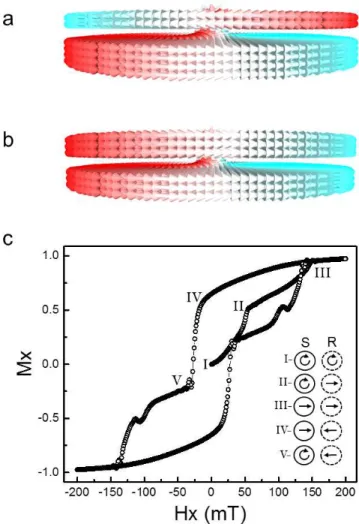
Two different configurations were compared. In the first one, the storage layer was chosen 4nm thick and the reference layer 2nm thick. In this case, after applying the out-of-plane field cooling protocole described above and despite the presence of the Oersted field from the setting current, it was found that in the relaxed remanent state, the two vortices have aligned core polarization but opposite chirality (Figure 2a). This can be explained by the dipolar interactions between the two vortex-cores and between the in-plane components of the two vortices exceeding the Oersted field due to the setting current. In a second configuration, the reference layer and storage layer were chosen with the same thickness of 3nm. After relaxing the structure as in the previous case, the chirality and polarization were found to be the same in both layers, as presented in Figure 2b. In order to study the stability of this double vortex configuration, a full hysteresis curve (Figure 2c) was simulated on this second structure assuming a damping of α=0.1. From this loop, the field necessary to annihilate the vortex in the soft reference layer can be estimated to be ~50mT and ~140mT for the pinned storage layer. On the decreasing hysteresis branch, it is important to note that the reference layer never switches back to vortex state. Once the vortex is annihilated, it does not appear again with in-plane field. This means that this configuration with two vortices of same chirality is quite metastable for these choice of thicknesses and that the procedure with out-of-plane field application is mandatory to initialize it. The field necessary to reverse the reference layer magnetization coming from positive saturation (after vortex annihilation i.e. when this layer is close to single domain state) is ~20mT.
The possibilities of multilevel storage using these two types of configurations (double vortex of opposite chirality or double vortex of same chirality) are compared below.
Fig. 2- Vortex configurations after the out-of-plane field cooling protocol. a) Structure in which the storage (S) layer is 4nm thick and reference (R) layer 2nm thick. At remanence, they exhibit opposite chirality and aligned polarization; b) Structure in which the storage and reference layer have the same thickness 3nm. At remanence, the two vortices have same chirality and polarization; c) Hysteresis loop calculated by micromagnetic simulation for the structure of b). Inset: the different configurations of magnetization under in-plane external field.
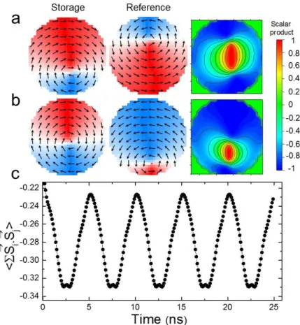
In the configuration with storage layer and reference layer in vortex configuration of opposite chirality (storage layer 4nm thick/reference layer 2nm thick), the writing process is performed by cooling down the system from its blocking temperature to RT under 20mT. After switching off the field, the storage layer magnetization remains in a shifted vortex configuration [23] as illustrated in figure 3a. For the reading process, AC currents in quadrature with frequency of 200 MHz are supposed to be applied in the orthogonal word and bit lines, in order to generate an in-plane rotating field of amplitude 20mT, enough to rotate the vortex core in the soft reference layer (Figure 3b). In MTJ, due to the TMR, the conductance varies as the cosine of the angle between the magnetization in the two magnetic electrodes. Here the two electrodes are in
inhomogeneous magnetic states so that a spatial integration must be performed of all local conductances to obtain the total MTJ conductance in a given configuration. The local conductances are given by the scalar product of the facing spins on both sides of the tunnel barrier. For convenience, we will work in the following with the magnetoconductance TMG knowing that the conductance is just the inverse of the resistance. The advantage of the TMG is that it is a linear function of the integrated scalar product between the local magnetization in the two ferromagnetic electrodes. The expression of the normalized TMG is the following:
=
∑ .,
(2)where iR and iS represents facing meshes from reference and storage layer in contact
with the tunnel barrier, and are the local magnetization orientations at these meshes, n is the total number of meshes in a layer. The TMG as defined in (2) varies between -1 and 1 corresponding respectively to full antiparallel and parallel configurations. Snapshots of storage and reference layer magnetization obtained during application of the rotating field corresponding respectively to the situations of maximum and minimum conductances are presented in Figures 3a and 3b together with the mapping of the local scalar products. The evolution of the TMG versus time is presented in Figure 3c.
Figure 3 – Snapshot of magnetization in pinned storage layer, reference layer magnetization under rotating field of 20mT and a) Configuration giving the maximum integrated scalar product between spins of both layers (maximum conductance), b) Configuration yielding the minimum integrated scalar product between spins of both layers (minimum conductance), c) Evolution of normalized TMG versus time.
From these results, it is possible in principle to derive the vortex position in the storage layer from the phase of the measured TMG signal. However, in this configuration where the two ferromagnetic layers have opposite vortex chirality, due to the relatively strong magnetostatic interactions between the two layers, the amplitude of the TMG signal is quite weak, of the order of 5% only of the full TMR signal. This value is too low for practical applications and would yield long read access time.
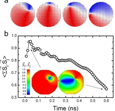
We next turn to the configuration where the storage layer and reference layer have same thickness (3nm). In this case, two vortices of same chirality can be stabilized thanks to the out-of-plane field cooling procedure. As a result, higher values of TMR can be expected since almost full local parallel alignment can be obtained when the two vortices lie on top of each other.
However, as previously noted from the hysteresis loop, this configuration is very unstable. When applying the rotating external magnetic field to read out the information, even a small rotating field of 10mT is enough to yield vortex annihilation in the reference layer after a few nanoseconds (less than one 360° rotation of the rotating field), as illustrated in Figure 4a. Figure 4b shows the time evolution of the TMG signal till the vortex annihilation. A variation close to 40% of TMG is obtained between the initial configuration and the vortex annihilation. The inset shows maps of the local scalar product (local conductance) in the initial configuration wherein the vortex cores are almost aligned and just before the vortex annihilation.
Figure 4 – Case wherein storage layer and reference layer have same thickness (3nm) and have been initialized with vortex of same chirality and polarity a) Snapshots of vortex annihilation in reference layer after 0.6ns under rotating field of 10mT and b) TMG time variation from the initial configuration wherein the vortex cores are almost aligned to the configuration just before vortex annihilation in the reference layer. The inset shows maps of local scalar product in the configurations yielding the highest and lowest conductance values.
In conclusion, the two configurations investigated in which the reference layer is in vortex configurations do not seem very practical either because of quite low readout signal (case of vortices of opposite chirality) or because of the instability of the vortex configuration during operation (case of vortices of same chirality).
Another option is then to use a reference layer in close to single domain configuration. This is described in the following section.
b) Storage layer in vortex configuration and soft reference layer in single domain configuration:
In a second approach, the thickness of the soft reference layer and/or its initializing procedure were chosen to set this layer in a configuration close to single domain. This configuration is not perfectly single domain due to the natural tendency of the magnetization to follow the pillar edges to minimize magnetostatic energy. However, in the following, we will call this state single domain for simplicity. In this case, after having applied the initializing protocol with out-of-plane field cooling to set the storage layer in vortex state, an in-plane field of 20mT is applied to annihilate the vortex which has formed in the reference layer.
After these initializations, the write procedure consists as before in heating the storage layer above its AF blocking temperature and cooling down the cell under a 20mT magnetic field. This results in a transverse shifting of the core of the storage layer vortex.
We first considered the cells in which the storage layer and reference layer have the same thickness 3nm.
In this case, due to the strong magnetostatic field created by the single domain reference layer on the storage layer during the field cooling procedure, the field cooling of the storage layer magnetization must be realized quite fast to avoid vortex annihilation during the cooling. In these simulations, the vortex state in the storage layer could be stabilized provided the heating/cooling procedure be faster than ~1ns which would be experimentally challenging. We will see later that by using thinner soft reference, this condition is removed thanks to the reduced magnetostatic field created by the reference layer on the storage layer.
Figure 5 illustrates some results obtained under these conditions. Different radial positions of the vortex core in the storage layer could be obtained by dynamically playing on the heating/cooling pulse duration while the vortex was dynamically moving from the center of the cell towards the edge before its annihilation. Several angular positions could also be obtained by varying the applied field directions, illustrated in Fig.5c by using Hx or Hy applied fields.
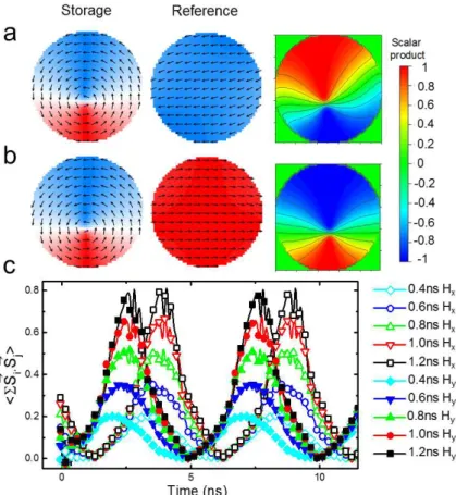
Figure 5 – Case of storage layer in vortex configuration and reference layer in single domain configuration, both 3nm thick. Snapshots of magnetization in storage layer and reference layer under rotating read field with a) configuration yielding maximum and b) minimum average scalar product between spins of both layers. c) Evolution of TMG signal vs time for different initial radial and angular positions of the vortex core obtained by varying the heating time between 0.4 – 1.2ns and field application directions (Hx (open dots) and Hy (closed dots)).
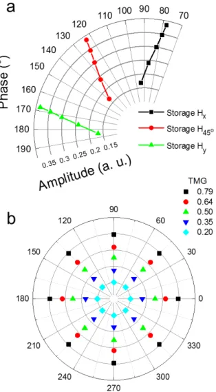
In order to extract the stored information contained in the amplitude and phase of the TMG readout signal, a Fourier transform of the TMG signal was performed for each vortex core position. The graph presented in Figure 6a, shows the amplitude and phase extracted after 25ns of reading for different vortex core positions obtained in the conditions of Fig.5c with field applied along x, y axes and along their diagonal. For a given direction of the applied field, a shift of the phase of the core by about 20° is observed as the vortex core is set further off-center. This is due to the dynamic motion of the core during the heating/cooling pulse under the influence of applied field and stray field from the reference layer. As the angular shift of the phase is the same for all written directions at each field value, this phase shift in principle does not affect how many states can be written. Concerning the TMG signal amplitude, it is interesting to note that the obtained amplitudes are much larger here than in the case where the
reference layer was also in vortex configuration. In the present case, the calculated difference of about 15% between the normalized TMG amplitude obtained in the 5 radial positions tested and 2 angular positions per quadrant, opens the possibility to obtain more than 40 states, represented in Figure 6b, in the same bit cell.
Figure 6 – a) Amplitude and phase calculated by Fourier transform of the TMG signal presented in Fig. 5c. b) Different schematic possible stored states representing the set vortex core positions in the storage layer at remanence and corresponding TMG amplitude depending on the radial position.
As mentioned previously, due to the strong magnetostatic field created by the reference layer in single domain state on the storage layer when these two layers are 3nm thick, the heating/cooling pulse during write must be quite short (<~1ns) to avoid the vortex annihilation in the storage layer. This would be rather difficult to implement experimentally since in typical TA-MRAM, the heating/cooling phase typically lasts for 10ns. In order to decrease the dipolar influence of the reference layer on the storage
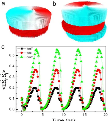
layer, as straightforward approach is to reduce the thickness of the reference layer. In the following, the reference layer thickness was decreased to 1.2nm. Simulations were performed with the same parameters as before, just with the mesh size changed to 3x3x0.3 nm. After applying the initial protocol to generate vortex in the storage layer, the magnetization ground state observed was directly in-plane single state magnetization in the reference layer and pinned vortex in the storage layer with the core slightly shifted due to the dipolar interaction with the reference layer (See Figure 7a). In order to further reduce the magnetostatic influence of the reference layer on the storage layer, a synthetic antiferromagnetic (SAF) reference layer was then used. The reference layer now consists of two antiferromagnetically coupled CoFe layers separated by a 0.9 nm Ru spacer providing an RKKY antiferromagnetic exchange coupling assumed to be equal to 1 mJ/cm2. The use of different CoFe layer thicknesses
in the two layers constituting the SAF (1.2nm for the layer the closest to the storage layer and 1.8nm for the other layer), allows decreasing the dipolar interaction with the storage layer while maintaining a net magnetization in the reference layer, which will be necessary for magnetization rotation, under external rotating magnetic field, during the readout process. The remanent state obtained after the initializing protocol is presented in Figure 7b. The vortex core is now well centered thanks to the reduced magnetostatic interaction between reference layer and storage layer. The simulation of storage and reading processes were the same as before, with rotating field lowered to 10mT. The vortex core was set at 3 different radial positions by applying write cooling field of 4, 5 and 6mT. Interestingly, thanks to the reduced magnetostatic interactions between reference layer and storage layer, there is no more requirement in the heating/cooling pulse duration to stabilize the vortex core position. The position of the vortex core in the storage layer can be set here as in conventional TA-MRAM with heating pulse of about 5 to 10ns. The obtained TMG signals under 10mT rotating read field are shown in Figure 7c. Since the vortices are written here in a quasistatic way and not in a dynamic way as before, no more shift in the vortex core angular position is observed as the radial off-centering of the core is increased. In addition, during the rotation of the soft reference layer magnetization, the vortex in the storage layer remains almost fixed which increases its stability upon reading. Due to these advantages, this configuration looks the most appropriate for implementation in practical devices.
Figure 7 – Case where the storage layer if in vortex configuration (3nm thick) and thinner reference layer in single domain state a) Remanent state when the reference layer consists of a single ferromagnetic layer 1.2nm thick. A vortex shift in the storage layer is still observed due to the dipolar interaction with the reference layer. b) Remanent state when the reference layer is part of a synthetic antiferromagnetic layer. The vortex in the storage layer is then centered in the initial state thanks to the reduced magnetostatic interaction with the SAF and c) Time evolution of theTMG signal under the rotating read field of 10mT for three radial positions of the storage layer vortex core obtained by field cooling in Hx= 4, 5 and 6mT.
Conclusion
We have proposed and investigated by micromagnetic simulations, a new approach for multilevel TA-MRAM design. It is based on the use of an exchange biased storage layer in vortex configuration. The information is encoded via the position of the vortex core which can be varied along two degrees of freedom: radius and angular position. Various configurations were studied and their advantages and drawbacks discussed. The best one among the investigated configurations is one in which the reference layer is a synthetic antiferromagnetic layer in single domain configuration in which the thickness of the two antiferromagnetically coupled ferromagnetic layers were adjusted to minimize the stray field on the storage layer. This configuration enables storage and
writing under magnetic fields below 10mT. From the results obtained by our simulations, the proposed TA-MRAM could support more than 40 different logic states, corresponding to at least 5 bits per cell.
Acknowledgements: This work was partly funded under ERC Adv grant n°669204 MAGICAL and Brazilian agency CNPq.
References
1 - T. Miyazaki and N. Tezuka, Giant magnetic tunneling effect in Fe/Al2O3/Fe
junction, J. Magn. Magn. Mater. 139, 231–234 (1995)
2 - J. S. Moodera, Lisa R. Kinder, Terrilyn M. Wong, and R. Meservey, Large Magnetoresistance at Room Temperature in Ferromagnetic Thin Film Tunnel Junctions, Phys. Rev. Lett. 74, 16, 3273–3276 (1995).
3 - A. Khvalkovskiy, D. Apalkov, S. Watts, R. Chepulskii, R. S. Beach, A. Ong, X. Tang, A. Driskill-Smith, W. H. Butler, P. B. Visscher, D. Lottis, E. Chen, V. Nikitin, and M. Krounbi, “Basic principles of STT-MRAM cell operation in memory arrays,” J. Phys. D. Appl. Phys.46, 7, 74001 (2013).
4 – L. Savtchenko, B. N. Engel, N. D. Rizzo, M. DeHerrera and J. Janesky, Method of Writing to Scalable Magnetoresistance Random Access Memory Element, US Patent Specification 6, 545, 906 B1 (2003)
5 – J. M. Slaughter, N. D. Rizzo, F. B. Mancoff, R. Whig, K. Smith, S. Aggarwal and S. Tehrani, Toggle and Spin-Torque MRAM: Status and Outlook, Journal of Magnetic Society of Japan, 5, 171 (2010)
6 – I. L. Prejbeanu, M. Kerekes, R. C. Sousa, H. Sibuet, O. Redon, B. Dieny and J. P. Nozières, Thermally assisted MRAM, Journal of Physics: Condensed Matter, 19, 16 (2007)
7 – I. L. Prejbeanu, W. Kula, K. Ounadjela, R. C. Sousa, O. Redon, B. Dieny, and J.-P. Nozieres, “Thermally Assisted Switching in Exchange-Biased Storage Layer Magnetic Tunnel Junctions,” IEEE Trans. Magn., vol. 40, no. 4, pp. 2625–2627, Jul. 2004
8 – B. Dieny, R. Sousa, S. Bandiera, M. Castro Souza, S. Auffret, B. Rodmacq, J. P. Nozieres, J. Hérault, E. Gapihan, I. L. Prejbeanu, C. Ducruet, C. Portemont, K.
Mackay, and B. Cambou, “Extended scalability and functionalities of MRAM based on thermally assisted writing,” IEEE Int. Electron Devices Meet., no. 33, pp. 11–14, 2011
9 – J. C. Slonczewski, Current-driven excitation of magnetic multilayer, Journal of Magnetism and Magnetic Materials, 159, 1-2 (1996)
10 – L. Berger, “Emission of spin waves by a magnetic multilayer traversed by a current,” Phys. Rev. B, vol. 54, no. 13, pp. 9353–9358, 1996.
11 – Y. Huai, F. Albert, P. Nguyen, M. Pakala and T. Valet, Observation of spin-transfer switching in deep submicron-sized and low-resistance magnetic tunnel junctions, Applied Physics Letters 84, 3118 (2004)
12 – K. C. Chun, H. Zhao, J. Harms, T. –H. Kim, J. –P. Wang and C. Kim, IEEE Journal of Solid-State Circuits 48, 598 (2013)
13 – W. S. Zhao, Y. Zhang, T. Devolder, J. O. Klein, D. Ravelosona, C. Chappert, P. Mazoyer, Microelectronics Reliability, 52, 1848-1852 (2012)
14 – Miron, I. M. et al. Current-driven spin torque induced by the Rashba effect in a ferromagnetic metal layer. Nature Mater. 9, 230–234 (2010).
15 – Miron, I. M. et al. Perpendicular switching of a single ferromagnetic layer induced by in-plane current injection. Nature 476, 189–193 (2011).
16 – Liu, L., Lee, O. J., Gudmundsen, T. J., Ralph, D. C. & Buhrman, R. A. Current induced switching of perpendicularly magnetized magnetic layers using spin torque from the spin Hall effect. Phys. Rev. Lett. 109, 096602 (2012).
17 – M. Cubukcu, O. Boulle, M. Drouard, K. Garello, C. O. Avci, I. M. Miron, J. Langer, B. Ocker, P. Gambardella and G. Gaudin, Spin-orbit torque magnetization switching of a three-terminal perpendicular magnetic tunnel junction, Applied Physics Letters 104, 042406 (2014)
18 – K. Garello, C. O. Avci, I. M. Miron, M. Baumgartner, A. Ghosh, S. Auffret. O. Boule, G. Gaudin and P. Gambardella, Ultrafast magnetization switch by spin orbit torques, Applied Physics Letters 105, 212402 (2014)
19 – T. Ishigaki, T. Kawahara, R. Takemura, K. Ono, K. Ito, H. Matsuoka, and H. Ohno, “A Multi-Level-Cell Spin-Transfer Torque Memory with Series-Stacked Magnetotunnel Junctions,” VLSI, pp. 234–235, 2010.
20 – I. L. Prejbeanu, Multibit magnetic random access memory cell with improved read margin. US Patent 20120155159
21 – Stainer, Q., L. Lombard, K. Mackay, D. Lee, S. Bandiera, C. Portemont, C. Creuzet, R.C. Sousa and B. Dieny, Self-referenced multi-bit thermally assisted magnetic random access memories, Applied Physics Letters 105 (2014) 032405. 22 – K.L.Metlov and Y.Lee, Map of metastable states for thin circular magnetic nanocylinders, Appl.Phys.Lett.92, 112506 (2008).
Note: In the present paper, we use as exchange length the standard expression in SI units given by 2 0 / 2 ex s ex A M L = µ (see
as definition 2 0 / 4 ex s
ex A M
L = π µ . Therefore the data of Ref.22 are transformed according to the standard definition of Lex for discussion in this paper.
23 – J. Sort, K. S. Buchanan, V. Novosad, A. Hoffman, G. Salazar-Alvarez, A. Bollero, M. D. Baró, B. Dieny, and J. Nogués, Imprinting Vortices into
Antiferromagnets, Physical Review Letters 97, 067201 (2006)
24 – A. Vansteenkiste, J. Leliaert, M. Dvornik, M. Helsen, F. G. Sanchez and B. V. Waeyenberge, The design and verification of MuMax3, AIP Advances 4, 107133 (2014)
25- K. Tanahashi, A. Kikukawa and Y. Hosoe, Exchange-biased CoTaZr soft underlayer for perpendicular recording, J. Appl. Phys. 93, 8161 (2003)
26 - K. Yu. Guslienko, V. Novosad, Y. Otani, H. Shima, and K. Fukamichi, Field evolution of magnetic vortex state in ferromagnetic disks, Appl.Phys.Lett.78, 3848 (2001).
27 - P. Wiśniowski, J. M. Almeida, S. Cardoso, N. P. Barradas, and P. P. Freitas,
Effect of free layer thickness and shape anisotropy on the transfer curves of MgO magnetic tunnel junctions, Journ.Appl.Phys. 103, 07A910 (2008).