HAL Id: hal-00635956
https://hal.archives-ouvertes.fr/hal-00635956
Submitted on 27 Oct 2011
HAL is a multi-disciplinary open access
archive for the deposit and dissemination of
sci-entific research documents, whether they are
pub-lished or not. The documents may come from
teaching and research institutions in France or
abroad, or from public or private research centers.
L’archive ouverte pluridisciplinaire HAL, est
destinée au dépôt et à la diffusion de documents
scientifiques de niveau recherche, publiés ou non,
émanant des établissements d’enseignement et de
recherche français ou étrangers, des laboratoires
publics ou privés.
Resistance switching in HfO2 metal-insulator-metal
devices
Patrice Gonon, Mathieu Mougenot, Christophe Vallée, Corentin Jorel,
Vincent Jousseaume, Hélène Grampeix, Fadhel El Kamel
To cite this version:
Patrice Gonon, Mathieu Mougenot, Christophe Vallée, Corentin Jorel, Vincent Jousseaume, et al..
Resistance switching in HfO2 metal-insulator-metal devices. Journal of Applied Physics, American
Institute of Physics, 2010, 107 (7), pp.074507. �10.1063/1.3357283�. �hal-00635956�
Resistance switching in HfO2 metal-insulator-metal devices
P. Gonon, M. Mougenot, C. Vallée, C. Jorel, V. Jousseaume et al.
Citation: J. Appl. Phys. 107, 074507 (2010); doi: 10.1063/1.3357283
View online: http://dx.doi.org/10.1063/1.3357283
View Table of Contents: http://jap.aip.org/resource/1/JAPIAU/v107/i7 Published by the American Institute of Physics.
Additional information on J. Appl. Phys.
Journal Homepage: http://jap.aip.org/Journal Information: http://jap.aip.org/about/about_the_journal Top downloads: http://jap.aip.org/features/most_downloaded Information for Authors: http://jap.aip.org/authors
Resistance switching in HfO
2metal-insulator-metal devices
P. Gonon,1,a兲M. Mougenot,1C. Vallée,1C. Jorel,1V. Jousseaume,2H. Grampeix,2 and F. El Kamel3
1
Microelectronics Technology Laboratory (LTM), Joseph Fourier University, French National Research Center (CNRS), 17 Avenue des Martyrs, 38054 Grenoble Cedex 9, France
2MINATEC, CEA-LETI, 17 Avenue des Martyrs, 38054 Grenoble Cedex 9, France
3Laboratory for the Organization and Properties of Materials (LMOP), El Manar University, Tunis 1060,
Tunisia
共Received 14 December 2009; accepted 3 February 2010; published online 9 April 2010兲
Resistance switching is studied in Au/HfO2共10 nm兲/共Pt, TiN兲 devices, where HfO2is deposited by
atomic layer deposition. The study is performed using different bias modes, i.e., a sweeping, a quasistatic and a static 共constant voltage stress兲 mode. Instabilities are reported in several circumstances 共change in bias polarity, modification of the bottom electrode, and increase in temperature兲. The constant voltage stress mode allows extracting parameters related to the switching kinetics. This mode also reveals random fluctuations between the ON and OFF states. The dynamics of resistance switching is discussed along a filamentary model which implies oxygen vacancies diffusion. The rf properties of the ON and OFF states are also presented共impedance spectroscopy兲. © 2010 American Institute of Physics.关doi:10.1063/1.3357283兴
I. INTRODUCTION
Resistance switching is a phenomenon by which some electrical insulators display a change in resistance upon ap-plication of a bias voltage. Such a phenomenon was ob-served several decades ago1 and has been widely studied in 1970s.2More recently, the subject gained a new interest for the fabrication of nonvolatile memories, named resistive ran-dom access memories共RRAMs兲. Last progresses in the field have been reviewed by Waser et al.3 Resistance switching has been observed in several classes of oxides, including binary metal oxides 共NiO, TiO2, ZrO2, CuxO, etc.兲,
perovs-kites 共BaTiO3, SrTiO3, etc.兲, and manganites
共Pr1−xCaxMnO3, La1−xSrxMnO3, etc.兲. Despite several years
of research efforts, the origin of resistance switching is still uncertain. Several models were proposed to explain the ef-fect, such as space charge limited currents, field-driven Mott insulator-metal transition, Schottky barrier modification at electrodes, or formation of conducting filaments upon field-enhanced migration of cations or anions across the film’s thickness共filamentary model兲.
In the filamentary model, oxygen vacancies seem to play an important role. A widely accepted mechanism is the following.3Oxygen is extracted from the oxide at the anode, leaving oxygen vacancies共VO2+兲 under the anode and oxygen ions 共O2−兲 within the anode 共oxide reduction, HfO
2
→HfO2−x+ xVO
2++ xO2−兲. Oxygen vacancies are drifted by
the electric field to the cathode and filaments containing VO2+ defects grow from the cathode to the anode. These filaments are conducting, possibly through carrier hopping between VO2+ related defects.4 When a filament comes into contact with the anode the electrodes are short-circuited and the de-vice switches in a conducting state 共ON state兲. When the voltage polarity is reversed, VO2+ are repelled from the anode
共former cathode兲, the filament in contact with the anode is broken, and the device switches back to an insulating state 共OFF state兲. Slight variants were proposed. For instance, it was outlined that since oxygen vacancies are positively charged, they never come into contact with the anode.3 In that case switching is viewed as a modulation of the filament tip/anode distance. When the VO2+ filament is in close prox-imity of the anode 共⬍2 nm兲 the ON state is established through a tunneling conduction between the filament tip and the anode. Conversely, when the filament tip/anode distance is large 共bias polarity is reversed兲, the device is in the OFF state.3This idea was recently developed in details by Pickett
et al.5 In the filamentary model, the ON-to-OFF transition requires to reverse the bias polarity 共bipolar device兲. How-ever, in many devices it is also observed that the OFF state can be restored by applying a bias of the same polarity 共uni-polar device兲. In such devices the ON-to-OFF transition is ascribed to Joule heating which leads to the thermal dissolu-tion of conducting filaments.
Compared to oxides so far studied for RRAMs, HfO2
has the advantage of being more mature from a technological point of view. This dielectric has been widely studied as a high-k gate oxide, and hafnium-based dielectrics are now being introduced for advanced Complementary Metal Oxide Semiconductor共CMOS兲 gates.6Therefore, as far as ease of integration is concerned, HfO2 would be an interesting can-didate for the RRAM technology. Some works on the resis-tance switching properties of HfO2 were recently
published.7–12Lee et al.10studied Ru/HfO2/TiN stacks and
postulated that switching occurs at the Ru/HfO2 interface whose properties are controlled by the amount of oxygen at this interface. The same authors recently introduced an AlCu buffer layer to improve memory performances.8 In Au/HfO2/Pt structures oxygen deficiency was observed at the HfO2/Pt interface.9 The above results show that the
metal/HfO2 interface plays an important role. Bulk
crystal-a兲Author to whom correspondence should be addressed. Electronic mail:
JOURNAL OF APPLIED PHYSICS 107, 074507共2010兲
linity appears as a significant parameter as well. In Pt/HfO2/Pt memory performances are enhanced upon
postannealing.11It was concluded that, in the ON state, con-ducting filaments are formed at grain boundaries.11Chan et
al.,12who studied Au/HfO2/Pt devices, reported that switch-ing proceeds in crystalline films, but not in amorphous ones. These authors attributed the switching to the migration of oxygen vacancies along grain boundaries. Walczyk et al.7 reported that reliable switching in Au/HfO2/TiN devices
was only observed in HfO2 films whose thickness is above
20 nm. Regarding switching polarity 共unipolar or bipolar兲, different results were published. HfO2films were reported to
be unipolar,7,10,11 bipolar,8 both unipolar and bipolar,9 or changing from unipolar to bipolar after oxygen annealing.12 This brief survey shows that more studies are needed to un-derstand resistance switching in HfO2.
In this work we study Au/HfO2/共Pt or TiN兲 structures.
Resistance switching is studied using different dc bias modes, i.e., a sweeping mode, a quasistatic mode, and a static共constant voltage stress兲 mode. The ac electrical char-acteristics of the ON and OFF states are also reported. The roles of the bias polarity, of the electrodes, and of the tem-perature in the stability of the ON state are underlined. In a constant voltage stress mode, an interesting behavior is ob-served. In this mode, the sample’s resistance is unstable, switching between the OFF and ON states as time elapses. Results are discussed along the oxygen vacancy-based fila-mentary model.
II. EXPERIMENT
HfO2 films 共10 nm兲 were grown at 350 °C by atomic
layer deposition 共ALD兲 using alternate cycles of H2O and
HfCl4precursors 共1 Torr兲 on Pt 共100 nm兲/Ti 共10 nm兲/Si wa-fers. For the purpose of comparison, some films were also deposited on TiN 共60 nm兲/Ti 共40 nm兲/Si wafers. Top gold electrodes共100 nm thick, 2 mm in diameter兲 were deposited on the HfO2films by dc-sputtering. Electrical measurements
共dc modes兲 were performed in air using a Keithley 2635 Source Meter unit, with the bottom electrode grounded. Dur-ing switchDur-ing from the OFF to the ON state the current is limited to 0.1 mA 共current compliance兲 to avoid samples breakdown. Impedance spectroscopy 共ac characteristics兲 were carried out using a Novocontrol analyzer working in the 1 Hz–100 kHz frequency range.
Structural properties of HfO2 films were studied using
angle-resolved x-ray photoelectron spectroscopy 共ARXPS兲, IR spectroscopy and ellipsometry. Results of these character-izations can be found elsewhere.13Briefly, it was found that the films are crystallized in the monoclinic phase. Their gap is around 5.5 eV. ARXPS performed on thinner films共2 nm兲 deposited on Pt reveals a homogeneous composition across the thickness with a sharp HfO2/Pt interface 共absence of PtO
oxides兲. On the contrary, films deposited on TiN show the presence of TiOxNyand TiO2at the HfO2/TiN interface.13
III. RESULTS AND DISCUSSION A. Sweeping mode
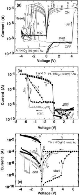
Resistance switching was first tested in a sweeping mode 共0.35 V/s兲. Results are shown in Fig. 1. Figure 1共a兲shows the characteristics of Au/HfO2/Pt stacks when submitted to “positive” bipolar cycles 共VAu/Pt= 0 V→7 V→0 V→ −4 V→0 V兲. Ten successive cycles are shown in Fig.1共a兲. Very good reproducibility is obtained for Vset 共+4 V兲, but large dispersion is observed for Vreset 共between ⫺1.5 and
⫺3.5 V兲. Unipolar cycles were also tested. A first cycle 共0 V→7 V→0 V, with current compliance兲 was applied to set the sample in the ON state. A second cycle 共0 V
→7 V→0 V, no current compliance兲 was applied in order
to reset the sample. However, such cycles systematically failed to restore the OFF state. In similar structures 共Au/HfO2/Pt stacks兲 both bipolar and unipolar behaviors
FIG. 1. I-V characteristics in a sweeping mode 共0.35 V/s兲 for 共a兲 Au/HfO2/Pt stacks when submitted to positive cycles 共0 V→+7 V
→0 V→−4 V→0 V兲, 共b兲 Au/HfO2/Pt stacks when submitted to
nega-tive cycles 共0 V→−7 V→0 V→+4 V→0 V兲, and 共c兲 Au/HfO2/TiN stacks when submitted to positive cycles 共0 V→+7 V→0 V→−4 V
→0 V兲. Cycles are numbered in sequence.
were reported,9 which is not observed here. As opposed to previous works,7,9,10 it is also noticeable that the present films do not require a forming step. Indeed, the Set at +4 V is recorded during the first voltage sweep.
In the OFF state it is observed that the current is constant as the voltage is varied 关see Fig. 1共a兲, OFF state兴. This is indicative of a capacitive current given by I = C共dV/dt兲. The capacitive current is related to the displacement current den-sity j = dD/dt, where D=0rE is the electric displacement
field. Capacitance 共C兲_ of the devices is around 5⫻10−8 F
共see Sec. III F兲. Considering that dV/dt=0.35 V/s, we ob-tain I⬇10−8 A, which is the order of magnitude observed
for I in the OFF state 关calculation is approximate because V共t兲 is not exactly a linear function, but a staircase one兴. The capacitive current 共OFF state兲 is observed until the voltage reaches Vset= +4 V exactly. At this point the device
sud-denly switches to the ON state. Since the delay time between two voltage increments is of 1 s, the abrupt OFF→ON tran-sition observed at Vset= +4 V suggests that near below Vset,
i.e at V = +3.7 V共the voltage that is applied before reaching +4 V兲, filament growth requires much more than 1 s. If not, field-enhanced conduction should be observable between the filament tip and the anode共this will be observed later when studying the quasistatic mode, see Sec. III D兲. The corollary is that at Vset= +4 V 共electric field of 4 MV/cm兲 filaments growth occurs in a time scale shorter than 1 s. This is con-sistent with Sec. III E, where it will be shown that filaments growth proceeds at a speed which varies exponentially with the electric field共diffusion of oxygen vacancies兲. Therefore, it can be concluded that filaments growth is almost null be-low Vset, and occurs at fast speed at Vset共threshold voltage兲.
A highly reproducible Vsetvalue from cycle to cycle, and
the absence of forming, indicate that the filaments are com-pletely “washed out” at each Reset. On the contrary case, i.e., if the Reset led to a partial rupture of filaments, we would expect to observe a varying Vsetfrom cycle to cycle
共we should at least observe a Vset value which decreases
from the first to the second cycle兲. At each Reset the fila-ments are fully destroyed, so at each Set the sample must be “formed” again. In a sense, each Set is a forming stage. It is believed that the small thickness of our samples 共10 nm兲 allows a complete disappearance of filaments at Reset. In previous works7–12the samples thickness is 20 nm or above, at Reset filaments are partially ruptured and Vset is lower
than the forming voltage.
The fact that Vresetis fluctuating during successive cycles is more puzzling. Variation in Vresetappears to be random, without any correlation to the cycle number, nor any link to the current level in the ON state. An example is shown in Fig.1. The ON current in both the third and the fourth cycle is higher than in the first cycle but Vreset 共fourth cycle兲 ⬍Vreset共first兲⬍Vreset共third兲. This shows that Vresetis not
re-lated to the resistance of the filament, or in another words to a Joule effect.
B. Role of bias polarity
Stability of the ON state depends on the bias polarity used to switch the device. A typical example is shown in Fig.
1共b兲. The device is the same as in Fig.1共a兲共Au/HfO2/Pt兲,
but a “negative” bipolar cycles is applied 共VAu/Pt= 0 V→ −7 V→0 V→+4 V→0 V兲. An OFF→ON transition is observed at somewhat higher values共Vset= −5 V兲. More im-portantly, the ON state is not stable and it is lost when the voltage is swept back to 0 V. During the first cycle the ON state is progressively lost, before the voltage comes back to 0 V 关cycle 1 in Fig. 1共b兲兴. During the second cycle the ON
state has a longer lifetime, and is lost only at short-circuit 关cycle 2 in Fig. 1共b兲兴. In the third cycle, the ON state is
recovered as soon as a negative voltage is applied, with no need to reach Vset= −5 V. Again, the ON state is lost when
coming back to 0 V关cycle 3 in Fig.1共b兲兴.
Why is the ON state not maintained for negative cycles? For negative cycles 关Fig. 1共b兲兴 oxygen vacancies are pro-duced at the Pt electrode and VO2+filaments grow from the Au electrode. The instability of the ON state indicates that VO2+ filaments grown on the Au top electrode are easily ruptured 关Fig.1共b兲兴, while those grown on the Pt electrode are stable 关Fig. 1共a兲兴. Several reasons can be imagined. The first one could be that the VO2+-metal binding energy is lower for Au than for Pt. This is confirmed by studies of metal adsorption energy on oxide surfaces which contain oxygen vacancies. For instance, in both MgO共Ref.14兲 and TiO2共Ref.15兲, the
Pt-VOenergy is higher than the Au-VObinding energy
共dif-ference can be as high as 50%, e.g., in MgO the Pt-VObond
energy is of 581 kJ/mol and is only of 311 kJ/mol for Au-VO兲.14Therefore, when filaments are grown on Au
共nega-tive cycles兲 it could be that VO 2+
easily “unstick” from Au as the voltage is decreased. A second reason could be related to O2− diffusion. When positive bias is applied on the top Au
electrode关positive cycles, Fig.1共a兲兴, O2− are extracted from
the device and outdiffuse to the atmosphere through the Au electrode or at its periphery
共
O2−→12O2+ 2 e−兲
. On thecon-trary, when positive bias is applied on Pt 关negative cycles, Fig. 1共b兲兴, O2− ions are buried in this electrode and they cannot escape from the sample because Pt is the bottom elec-trode. When the electric field is removed共V=0 V兲, O2− dif-fuses back from the Pt electrode and leads to the rupture of VO2+ filaments 共O2−+ VO2+→OO兲. Finally, as suggested by
Jeong et al.,16oxygen diffusion through the Au top electrode can also retard the accumulation of oxygen vacancies at this electrode共1/2O2+ 2e−+ VO
2+→O
O兲. For negative cycles, the
above hypotheses suggest that the filaments are partially rup-tured at their extremity 共at the Au-VOinterface because of
weak Au-VO interaction or O2 diffusion, or at the Pt-VO
interface because of O2− back-diffusion from Pt兲.
C. Role of bottom electrode
Figure1共c兲shows the current-voltage 共I-V兲 characteris-tics recorded for a TiN bottom electrode 关keeping the same bias polarity as in Fig.1共a兲兴. In this case it is difficult to reset the device. Cycle 1 shows a Set at +4 V, but it is not pos-sible to get a Reset at V⬍0. Reset is obtained during the second cycle, but the OFF state is unstable, and the device comes back to the ON state while pursuing the sweep toward negative voltages. Finally, after a few cycles the device breakdowns 关cycle 6 in Fig. 1共c兲兴. The affinity of the metal
共TiN兲 to oxygen could play a role. Because TiN has a strong affinity for oxygen, it could lead to oxygen depletion in the oxide, thereby creating a large amount of oxygen vacancies close to the interface. This in turn could explain that stronger filaments are formed, which are more difficult to reset.
It is also noted that switching共first cycle兲 does not pro-ceed as abruptly as for Pt bottom electrodes. Instead, the OFF-to-ON transition is progressively established between 4 and 6 V关Fig.1共c兲兴. Finally, for V⬍4 V, a capacitive current is no longer observed, suggesting that other conduction mechanism dominates 共such as electron injection from the TiN electrode兲. This is consistent with the fact that the work function of TiN共5.1 eV兲 is lower than the Pt work function 共5.65 eV兲.
In these samples it was shown by ARXPS that the TiN/HfO2 interface contains a 2 nm interfacial layer
com-posed of TiOxNyand TiO2phases.13Before HfO2deposition
the TiN wafers were exposed to air and it is indeed known that upon exposure to air TiN oxidizes spontaneously to form TiO2at its surface.17Thus, the structure must be viewed as a TiN/TiOxNy共2 nm兲/HfO2 共10 nm兲/Au stack. At present the role played by the mixed TiOxNyinterfacial layer is unclear. Its adverse effect is to impede the Reset. It must be under-lined that this behavior radically differs from the one ob-served in Ref.7where good and stable switching character-istics are recorded for Au/HfO2/TiN stacks 共which also
contain a TiON interfacial layer at the bottom electrode兲. However, in Ref. 7 thicker films were used 共⬎20 nm兲 and the authors pointed out that “unreliable” behavior was ob-served for thinner films共without any further details兲. Here 10 nm films are used, which may be considered as consistent with this observation.
Because we were unable to obtain reliable switching characteristics with TiN, the rest of this paper will discuss only the data corresponding to the Au/HfO2/Pt stacks.
D. Quasistatic mode
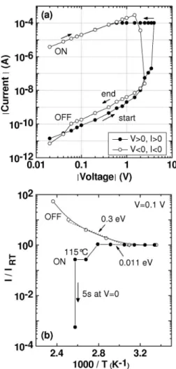
Resistance switching was further tested in a quasistatic mode关Fig.2共a兲兴. In this mode the voltage is increased every
1 min and the current is read at the end of this time interval. In that case bulk polarization has time to establish, the dis-placement current vanishes 共D=0E + P = const., dD/dt=0兲 and we observe the conduction current. The I-V characteris-tic is almost Ohmic up to 1 V and becomes supralinear above 1 V. Again, the device switches at Vset= +4 V exactly. How-ever, compared to the sweeping mode, the current steeply rises when reaching voltages close to Vset. For instance, at
V = +3.5 V the current in the quasistatic mode关Fig.2共a兲兴 is 100 times higher than in the sweeping mode 关Fig. 1共a兲兴. Since 1 min is left after each voltage step共instead of 1 s in the sweeping mode兲, it is believed that above 1 V the fila-ments have time to partially grow. For such a situation the conduction is enhanced because it occurs between the anode and the filaments tips where the electric field is reinforced. Since at V = +3.5 V the device is still in the OFF state, it means that at V = +3.5 V the filaments need more than 1 min to grow from the cathode to the anode. This has to be
com-pared to less than 1 s at V = +4 V 共see discussion in Sec. III A兲. These orders of magnitude will be confirmed later 共Sec. III E兲.
In Fig. 2共a兲 the Reset part of the I-V curve共V⬍0兲 is superimposed on the Set part 共V⬎0兲 to show that after the ON→OFF transition the OFF conduction level is the same as the one measured before the OFF→ON transition. This further supports the view that the filaments are totally de-stroyed at each Reset.
The temperature dependence of the OFF and ON states is depicted in Fig. 2共b兲 共25 °C⬍T⬍150 °C兲. During these measurements a constant bias of 0.1 V is maintained on the Au electrode 共Ohmic part of the OFF and ON states兲. Once the desired temperature is reached the sample is left for three minute to stabilize, and the current is measured. In the OFF state the I共T兲 curve departs from an Arrhenius law and a single activation energy cannot be observed. At 1000/T = 2.8 K−1共85 °C兲 the slope of the I共1/T兲 curve is around 0.3
eV. Walczyk et al.7observed the same activation energy and they ascribed it to an interstitial H related trap located at 0.3 eV below the conduction band. In Fig. 2共b兲 the absence of single activation energy indicates a distribution of states 共band tail兲 around 0.3 eV.
In the ON state the activation energy is very low 共11 meV兲 and it is consistent with an tunnel hopping conduction
FIG. 2. 共a兲 I-V characteristic in a quasistatic mode 共current is read 1 min after application of the bias voltage兲 and 共b兲 temperature dependence of the ON and OFF states共3 min temperature steps兲. The current 共I兲 is normalized to the room temperature current共IRT兲.
between localized states 共vacancy related defects兲.4 When reaching temperatures around 100 ° C the ON conductance 共G兲 decreases. If the sample is short-circuited during a few seconds at 115 ° C the conductivity drops over three decades 关Fig.2共b兲兴 to reach conductivity only one decade above the OFF state at the same temperature. This shows that the ON state is thermally unstable. Such instability can be under-stood by considering that thermal agitation acts again VO2+ alignment by the electric field. If the electric field is removed 共sample is short-circuited兲, the field-induced filamentary structure can no longer be maintained and thermal agitation leads to a rapid dissolution of the filaments. Note that to observe such a rapid loss of the ON state共in a few seconds兲 it is necessary to go above 100 ° C. At room temperature the devices retain the ON state up to one day 共the maximum retention period which was tested兲.
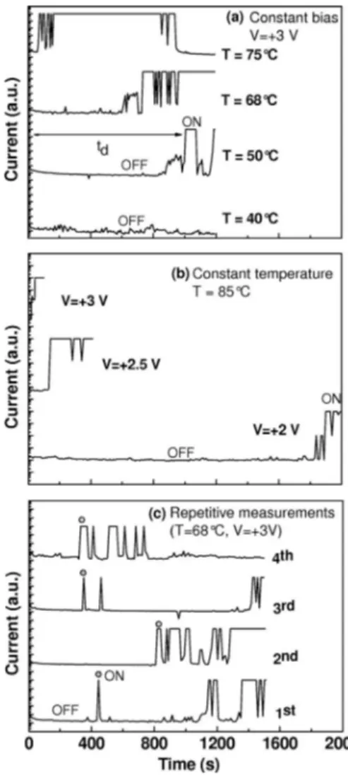
E. Static†constant voltage stress „CVS…‡ mode
In the preceding sections the filaments formation kinet-ics was evoked to explain the abrupt OFF→ON transition observed in the sweeping mode, as well as the high current levels observed near below Vset in a quasistatic mode. To
gain more information on filaments formation kinetics the samples were studied under a CVS mode. A first series of experiments was conducted by applying a constant positive bias of +3 V to the Au/HfO2/Pt stack and the current was
recorded as a function of time, at different temperatures共Fig.
3兲. Despite the fact that the bias 共+3 V兲 is below Vset
共+4 V兲, at a certain time the sample switches to the ON state. The first switch共OFF→ON兲 is followed by successive switches between the OFF and the ON states, with random time intervals separating two switching events. In Fig.3, it is apparent that the time to the first OFF→ON transition de-creases as the temperature inde-creases. In the following, this time共first OFF→ON transition兲 will be denoted the “delay time”共td兲.
In Fig.3, at each temperature a new共virgin兲 dot is used. We then performed successive CVS measurements on the same dot关Fig.4共a兲兴. At each new temperature, before record-ing the I共t兲 the sample is reset by applyrecord-ing a positive bipolar cycle as the one used in Fig. 1共a兲 共Sec. III A兲. It is often argued that Reset occurs by a partial rupture of filaments. Thus, by using the same dot we expected to observe a
de-crease in the time to the first switching 共td兲, because only a
part of the filament has to be reconstructed at each new ex-periment. This is not observed. When experiments are per-formed on the same dot the delay time tdis as long as the one
measured for fresh dots关sometimes even larger, compare T = 70 ° C in Fig. 3 and T = 68 ° C in Fig. 4共a兲兴. Again, this shows that a Reset restores the sample in a “fresh” state.
Figure5共a兲shows that td is thermally activated with an
activation energy around 1 eV. Within the hypothesis that the ON state corresponds to VO2+path extending from the cathode to the anode, then td is controlled by the slowest process
FIG. 3. I共t兲 recorded at a constant bias of +3 V, at different temperatures. A virgin dot is used at each temperature.
FIG. 4. I共t兲 characteristics recorded on the same dot, 共a兲 at constant bias and different temperatures,共b兲 at constant temperature and different biases, and 共c兲 at constant temperature and bias, at different times.
FIG. 5. Delay time共td兲 plotted 共a兲 as a function of temperature at constant
bias and共b兲 as a function of bias at constant temperature.
which takes part in the growth of the vacancy path. By re-ferring to works on metallic dendrites growth in electrolytes18 and to time-dependent switching in phase change memories 共PCRAMs兲,19 the growth rate of vacancy filaments could be limited by the production of vacancies at the anode, to their nucleation at the cathode,19 or to their diffusion in the bulk.18At present it is not possible to con-clude on which of the above mechanisms controls td. Let us
assume that VO2+diffusion is the rate limiting step. Following Barton and Bockris,18 the dendrites growth rate 共v兲 in ionic solutions is proportional to the diffusion coefficient 共D兲 of metal ions 共Eq. 8 in Ref. 18兲. By analogy, we should have
td⬃1/v⬃D−1, where D is the vacancy diffusion coefficient.
It is expected that the diffusion barrier is lowered as the electric field is increased. This is observed in Fig.4共b兲where tddecreases as the bias is increased. Figure5共b兲shows that td
varies exponentially with V as td⬃exp共−V/V0兲, where V0
= 0.21 V 共T=85 °C兲. These results are consistent with a field-enhanced diffusion for which D = D0 x exp共-Ea/kT兲 with Ea= Ea0-qFs, where Ea0is the activation energy at zero
field, F is the electric field, and s is the hopping distance of VO2+共q=2 e兲. The term 共qFs兲 represents the barrier lowering due to the electric field. Since F = V/t, where t is the film’s thickness, we have V0= tkT/qs. At T=85 °C, V0= 0.21 V
corresponds to s = 7 Å. At V = +3 V we measured Ea = 1.05 eV关Fig.5共a兲兴. Using s=0.7 nm, the barrier lowering
at +3 V is 0.44 eV, thus Ea0⬇1.5 eV 共intrinsic energy bar-rier for vacancy hopping in absence of electric field兲. We are not aware of experimental data about VO2+diffusion in HfO2.
A theoretical study20 predicts that the activation energy for VO2+ long-range diffusion in HfO2is around 0.7 eV, well
be-low the value found here. Barriers of 1.5 eV were calculated for jumps between neighbored sites,20but they do not corre-spond to the lowest energy diffusion path共0.7 eV兲 which is the one that should be observed experimentally. More elabo-rated models of dendrite growth21 may provide a better de-scription of the present data, but they require numerical solv-ing and they were not considered here.
It is interesting to note that a similar law 关td⬃exp共 −V/V0兲兴 was recently reported for time-dependent switching in conductive bridging memories共CBRAMs兲 using the dif-fusion of Ag in a-Si.22 This points to the similarity of the mechanism involved in both RRAMs and CBRAMs 共diffu-sion of cations, the cations being VO2+in the present case, and Ag+in Ref.22兲. In Ref.22the time t
d共which was named the
“wait” time兲 was found to follow a Poisson distribution. In PCRAMs, Karpov et al.19 also reported a narrow dispersion of td which was ascribed to heterogeneities of the glassy
material. Figure 4共c兲 shows repetitive measurements per-formed on the same dot共at T=68 °C and V=+3 V兲. Some dispersion is indeed observed, but tdkeeps the same order of
magnitude during successive measurements. These data are consistent with a deterministic mechanism共diffusion兲 which is pertubated by some extra parameters, leading to a distri-bution of td around a central value. Dispersion in td values
may result from the fact that VO2+ filaments start growing from different electrode sites共i.e., different nucleation times must be taken into account兲, or that they follow different paths in the HfO2film共polycrystalline兲. The distribution law
was not studied and will be the subject of a future work. Therefore, the quoted value of 1.5 eV for Ea0should only be considered as a rough estimate.
Within the above model, at a given temperature it is possible to extrapolate the ratio of switching times for two different biases, i.e., td共V1兲/td共V2兲=exp关共−qs/tkT兲ⴱ共V1
−V2兲兴. At 300 K this relation gives td 共V=+3.5 V兲/td共V=
+4 V兲⬇17. In the preceding sections we concluded that the switching time at +3.5 V is above 60 s, and less than 1 s at +4 V, which would give td 共V=+3.5 V兲/td共V=+4 V兲 ⬎60. Obviously the values are not the same, but the order of magnitude is close. The ratio td 共V=+3.5 V兲/td共V=+4 V兲
= 60 would correspond to s = 10.6 Å and Ea= 0.75 eV in Fig. 5共a兲共instead of 7 Å and 1.05 eV兲. Discrepancy results from the lack of the precise determination of Eawhich would re-quire to study the statistical distribution of tdat various tem-peratures. Nevertheless, Ea is well above the activation
en-ergy related to the conduction in the OFF state 关around 0.3 eV, Fig.2共b兲兴. It shows that the traps which control the con-duction in the OFF state are not implied in the switching process.
We now turn back to the random switching events ob-served after the first switch 共t⬎td兲. In the sweeping mode
关Fig.1共a兲兴 the samples have a bipolar behavior. The Reset is
obtained only at negative voltages. However, in the CVS mode 共Fig.3兲 the Reset is obtained for a constant, positive
voltage. In that case it is believed that thermal dissolution of the conducting filaments occurs. This is possible if Joule heating is large enough for oxygen vacancies to migrate out of the filaments. Large Joule heating is produced by rising the temperature 共above 50 °C in Fig.3兲 and by leaving the
film under a constant current stress. Therefore, in the CVS mode the thermal motion of VO2+ 共filament rupture兲 con-stantly opposes the effect of the electric field 共alignment of VO2+ in a filamentary structure兲. This explains the fluctuation between the ON and OFF states reported in Figs.3and4. In the sweeping mode共Fig.1兲, rupture of conducting filaments
does not occur because Joule heating is too brief. More ex-actly, by referring to the work of Russo et al.,23 we can postulate that the sweeping rate共0.35 V/s兲 does not provide enough time for a thermal dissolution to take place. More-over, as sweeping mode experiments are carried out at room temperature 共Fig.1兲 heat evacuation is enhanced.
The signal observed in the CVS mode bears close resem-blance to random telegraph switching noise 共RTSN兲 ob-served, for instance, in Metal-SiO2-Si devices24or in metal-a-Si:H-metal devices.25In these devices RTSN was ascribed to the random filling-emptying of trap levels24 and to the random motion of hydrogen,25 respectively. In a-Si:H, Lust and Kakalios25 modeled RTNS by a dynamical percolation network where the random movement of hydrogen lead to the creation or elimination of conducting pathways. Percola-tion networks were recently put forward to explain resistance switching in TiO2.26 Therefore, oxygen vacancies in HfO2
could play a similar role to hydrogen in a-Si:H, and random events observed here in the CVS mode could be explained by a dynamical percolation network where VO2+ migration opens or closes conducting filaments. Finally, in SiO2it was
recently demonstrated that oxygen vacancies are at the origin
of the random telegraph signal 共RTS兲 noise observed in the prebreakdown regime.27 In SiO2, a recent theoretical work also shows that breakdown could arise from the percolation of oxygen vacancies.28 Thus, in oxides it is more and more apparent that resistance switching and breakdown phenom-ena are intimately related.
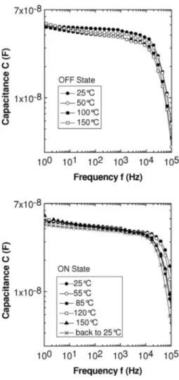
F. Impedance spectroscopy
Impedance spectroscopy was carried out to gain more information on the ON and OFF states. Figure6 shows the frequency dependence of the C and G for the ON and OFF states, as a function of the dot size. Figures7and8depict C and G as a function of temperature, for both states. During these experiments an ac amplitude of 0.1 Vrms was used 共much lower than Vsetand Vresetso as to not modify the state
of resistance兲.
In the OFF state G increases with frequency in a manner which is typical of insulators where an hopping conduction 共electronic or ionic兲 takes place, i.e., G=Gdc+ G0n, where
Gdcis the G in the dc regime, n is an exponent which usually
ranges between 0.5 and 1, and G0 is a prefactor.29Below 1
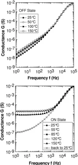
kHz, n is found to be around 0.8–0.9, decreasing with tem-perature 共0.93 at 50 °C and 0.81 at 150 °C, Fig.8兲. In the
same frequency range, C very slightly decreases with fre-quency, and slightly decreases with T共Fig.7兲.
Above 1 kHz the G共f兲 slope increases to reach n=1.8, independent of temperature. At the same time C drops 共f ⬎10 kHz兲. This could be interpreted as a dielectric relax-ation. However, the n value 共1.8兲 is much too high to be realistic 共n⬍1兲.29 Relaxations related to ions motion with n close to 2 has been observed in glasses, but at much higher frequencies 共f⬎GHz兲.30 While studying the resistance switching in Pr0.7Ca0.3MnO3 oxides, Das et al.31 reported a similar drop in C above 100 kHz which was ascribed to carriers relaxation at deep traps. Contrary to this explanation, here it is thought that the dispersion observed at f⬎1 kHz is due to a series resistance. Let be Rs this series resistance
共RsⰆR, where R=1/G is sample’s resistance兲. Calculation
shows that the total G is given by Gt= RsC22 共fc1ⰆfⰆfc2兲
and Gt= 1/Rs 共fc2Ⰶf兲, where fc1= 1/关2共RRs兲1/2C兴 and fc2
= 1/共2RsC兲. At the same time, the total C is given by Ct
= C共fc1ⰆfⰆfc2兲 and Ct= 1/Rs2C2共fc2Ⰶf兲. A quick look at
Fig.7shows that fc2⬇104 Hz, while a look at Fig.8shows
that fc1⬇103 Hz. Because C slightly decreases with f, the
expression Gt= RsC22 explains why we observe Gt⬃n
with n close to 2共n=1.8 gives C⬃f−0.1with the hypothesis
that Rsdoes not vary with f兲. The series resistance is thought
to come from the deposited top electrode 共rf-sputtered Au兲. Indeed, this electrode was observed by Secondary Electron Microscopy 共SEM兲 to have a granular structure, which may be at the origin of a significant resistance. Since Gt= 1/Rs
共fc2Ⰶf兲, the value of Rscan be deduced from the saturation
FIG. 6. Frequency dependence of the C and G in the ON and OFF states, as a function of the top electrode size.
FIG. 7. C in the OFF and ON states, as a function of temperature.
value of the G at high frequencies. In Fig. 8 beginning of saturation is observed around 100 kHz, from which we roughly estimate Rsto be in the 10– 100 ⍀ range.
Because of the series resistance only the data below 1 kHz should be considered to be representative of the oxide 共the data above 1 kHz will now be dismissed兲. In the ON state Fig.6shows that C varies like the electrode area. This figure also shows that CONis the same as COFF. On the con-trary, in the ON state G is independent of the electrode area. This confirms that conduction in the ON state proceeds through tiny filaments whose section is much smaller that the electrode diameter. It is also seen that GONis constant with frequency共plateau兲, at least up to 1 kHz 共dispersion above 1 kHz is due to the series resistance兲. Thus, if an hopping conduction proceeds through VO2+ defects its cut-off fre-quency should be well above 1 kHz. The GON value
mea-sured by impedance spectroscopy共between 10−4and 10−5 S兲
agrees with the current values measured in a sweeping mode 关between 10−4 and 10−5 A at 1 V, see Fig.1共a兲兴. From these
results, the device can be simply described by a ROFF 储C cell
for which ROFFis shunted by RONwhen the device is in the
ON state.
Figure7confirms that CONis the same as COFF共most of
the HfO2bulk is not affected by switching兲, and that CONis
stable with temperature. In Fig.2it was observed that RONis
unstable with temperature. This is again observed in Fig.8.
共ON state兲. At 150 °C GON decreases. While the sample is
cooled down to 25 ° C, the sample共which is short-circuited by the impedance meter during the cooling stage兲 returns back to a high resistance state共about one order of magnitude above the OFF state兲, consistent with a thermal dissolution of the conducting filaments as discussed previously.
IV. CONCLUSION
Resistance switching was studied in 10 nm HfO2 films deposited by ALD. The following conclusions were reached: • Regarding general properties, Au/HfO2 共10 nm兲/Pt stacks provide good resistance switching characteris-tics 共ON/OFF ratio⬎104, very reproducible V
set,
ab-sence of forming兲. However, Vreset shows dispersion.
The very low activation energy of the ON state 共11 meV兲 is compatible with a tunnel conduction 共hopping between VO2+兲. The device can only be reset by apply-ing negative biases 共bipolar only兲. Conduction in the OFF state is controlled by a distribution of traps around 0.3 eV. The memory can be described by a RC parallel cell where C is the same for the ON and OFF states, and ROFF is shunted by RON in the ON state
共filamentary conduction兲. No noticeable dispersion of ac characteristics is observed until 1 kHz. Dispersion above 1 kHz is due to electrode artifacts共series resis-tance兲. Important characteristics for integration, such as endurance and retention time over long periods, were not addressed and need to be studied in a future work.
• Instabilities of various kinds were observed. The ON state is not maintained for “negative cycles,” i.e., when vacancy filaments are grown on the Au electrode. This behavior was ascribed to a weak Au-VO binding en-ergy, or to the back-diffusion of O2−from the buried Pt
electrode. Reset is not possible when using a bottom TiN electrode. This is a serious drawback for future integration. Toward this goal, more work is needed to understand the role played by the TiOxNy interfacial
layer. Finally, it was noted that the ON state is ther-mally unstable共⬎100 °C兲. Such an instability can be explained by the thermal dissolution of vacancy fila-ments.
• Switching dynamics can be studied by comparing dif-ferent bias modes. The CVS mode reveals interesting features. The delay time to the first switch is found to be thermally activated and to vary exponentially with the voltage. This is consistent with a filament growth which is governed by VO2+diffusion共activation energy around 1.5 eV兲. After the first switch, ON-OFF transi-tions randomly occur in time, quite similar to RTS usually observed in prebreakdown regimes. It was pro-posed that these random instabilities result from a competition between the thermal dissolution of VO2+ filaments and their reconstruction upon the alignment of VO2+along the electric field.
1T. W. Hickmott,J. Appl. Phys.33, 2669共1962兲.
2See, for instance,IEEE Trans. Electron Devices 20, 89共1973兲 special
FIG. 8. G in the OFF and ON states, as a function of temperature.
issue on amorphous semiconductor devices, edited by A. I. Bienenstock, C. W. Bates, and W. Spicer.
3R. Waser, R. Dittmann, G. Staikov, and K. Szot,Adv. Mater.21, 2632
共2009兲.
4B. Gao, B. Sun, H. Zhang, L. Liu, W. Liu, R. Han, J. Kang, and B. Yu, IEEE Electron Device Lett.30, 1326共2009兲.
5M. D. Pickett, D. B. Strukov, J. L. Borghetti, J. J. Yang, G. S. Snider, D.
R. Stewart, and R. S. Williams,J. Appl. Phys.106, 074508共2009兲. 6A. Kerber and E. A. Cartier,IEEE Trans. Device Mater. Reliab.9, 147
共2009兲.
7Ch. Walczyk, Ch. Wenger, R. Sohal, M. Lukosius, A. Fox, J. Dabrowski,
D. Wolansky, B. Tillack, H.-J. Müssig, and T. Schroeder,J. Appl. Phys. 105, 114103共2009兲.
8H. Y. Lee, P.-S. Chen, T.-Y. Wu, Y. S. Chen, F. Chen, C.-C. Wang, P.-J.
Tzeng, C. H. Lin, M.-J. Tsai, and C. Lien,IEEE Electron Device Lett.30,
703共2009兲.
9S. Lee, W.-G. Kim, S.-W. Rhee, and K. Yong,J. Electrochem. Soc.155,
H92共2008兲.
10H. Y. Lee, P. S. Chen, T. Y. Wu, C. C. Wang, P. J. Tzeng, C. H. Lin, F.
Chen, M.-J. Tsai, and C. Lien,Appl. Phys. Lett.92, 142911共2008兲. 11Y.-M. Kim and J.-S. Lee,J. Appl. Phys.104, 114115共2008兲.
12M. Y. Chan, T. Zhang, V. Ho, and P. S. Lee,Microelectron. Eng.85, 2420
共2008兲.
13C. Jorel, C. Vallée, E. Gourvest, B. Pelissier, M. Kahn, M. Bonvalot, and
P. Gonon,J. Vac. Sci. Technol. B27, 378共2009兲.
14K. M. Neyman, C. Inntam, A. V. Matveev, V. A. Nasluzov, and N. Rösch, J. Am. Chem. Soc.127, 11652共2005兲.
15X.-Q. Gong, A. Selloni, O. Dulub, P. Jacobson, and U. Diebold,J. Am. Chem. Soc.130, 370共2008兲.
16D. S. Jeong, H. Schroeder, U. Breuer, and R. Waser,J. Appl. Phys.104,
123716共2008兲.
17J. Zimmermann, M. W. Finnis, and L. Colombi Ciacchi,J. Chem. Phys. 130, 134714共2009兲.
18J. L. Barton and J. O’M. Bockris,Proc. R. Soc. London, Ser. A268, 485
共1962兲.
19I. V. Karpov, M. Mitra, D. Kau, G. Spadini, Y. A. Kryukov, and V. G.
Karpov, Appl. Phys. Lett. 92, 173501 共2008兲; V. G. Karpov, Y. A.
Kryukov, M. Mitra, and I. V. Karpov,J. Appl. Phys.104, 054507共2008兲. 20N. Capron, P. Broqvist, and A. Pasquarello,Appl. Phys. Lett.91, 192905
共2007兲.
21C. Monroe and J. Newman,J. Electrochem. Soc.150, A1377共2003兲. 22S. H. Jo, K.-H. Kim, and W. Lu,Nano Lett.9, 496共2009兲.
23U. Russo, D. Ielmini, C. Cagli, and A. L. Lacaita,IEEE Trans. Electron Devices56, 186共2009兲.
24K. R. Farmer, C. T. Rogers, and R. A. Buhrman,Phys. Rev. Lett.58, 2255
共1987兲.
25L. M. Lust and J. Kakalios,Phys. Rev. Lett.75, 2192共1995兲.
26S. C. Chae, J. S. Lee, S. Kim, S. B. Lee, S. H. Chang, C. Liu, B. Kahng,
H. Shin, D.-W. Kim, C. U. Jung, S. Seo, M.-J. Lee, and T. W. Noh,Adv. Mater.20, 1154共2008兲.
27X. Li, C. H. Tung, K. L. Pey, and V. L. Lo,Appl. Phys. Lett.94, 132904
共2009兲.
28J. Kang, Y.-H. Kim, J. Bang, and K. J. Chang,Phys. Rev. B77, 195321
共2008兲.
29D. L. Sidebottom,Phys. Rev. B61, 14507共2000兲.
30K. Funke and R. D. Banhatti,Solid State Sci.10, 790共2008兲.
31N. Das, S. Tsui, Y. Y. Xue, Y. Q. Wang, and C. W. Chu,Phys. Rev. B78,
235418共2008兲.