HAL Id: hal-03240341
https://hal.archives-ouvertes.fr/hal-03240341
Submitted on 28 May 2021
HAL is a multi-disciplinary open access
archive for the deposit and dissemination of
sci-entific research documents, whether they are
pub-lished or not. The documents may come from
teaching and research institutions in France or
abroad, or from public or private research centers.
L’archive ouverte pluridisciplinaire HAL, est
destinée au dépôt et à la diffusion de documents
scientifiques de niveau recherche, publiés ou non,
émanant des établissements d’enseignement et de
recherche français ou étrangers, des laboratoires
publics ou privés.
Scanning Acoustic Microscopy versus Colored
Picosecond Acoustics to detect interface defects in
hybrid wafer bonding
Solene Bossut, Arnaud Devos, S Lhostis, E Deloffre, C Euvrard, F Dettoni, C
Chaton
To cite this version:
Solene Bossut, Arnaud Devos, S Lhostis, E Deloffre, C Euvrard, et al.. Scanning Acoustic Microscopy
versus Colored Picosecond Acoustics to detect interface defects in hybrid wafer bonding. Forum
Acusticum, Dec 2020, Lyon, France. pp.2553-2554, �10.48465/fa.2020.0878�. �hal-03240341�
Scanning Acoustic Microscopy versus Colored Picosecond
Acoustics to detect interface defects in hybrid wafer bonding
S. Bossut
a,b, A. Devos
a, S. Lhostis
b, E. Deloffre
b, C. Euvrard
b, F. Dettoni
band C. Chaton
ba IEMN, UMR CNRS 8520, Villeneuve-d’Ascq, 59650 Villeneuve-D’Ascq, France b STMicroelectronics, 850 rue Jean Monnet, 38926 Crolles Cedex, France
arnaud.devos@isen.iemn.univ-lille1.fr
ABSTRACT
3D integration offers the opportunity for microelectronic devices to gain die surface and efficiency. The highest interconnection pitch is obtained using hybrid bonding stacking. In this study a femtosecond laser in a pump-probe configuration is used to detect the bonded copper pads interface defects. The results are compared with Scanning Acoustic Microscope (SAM) measurements and both techniques are shown to be consistent.
1. INTRODUCTION AND BACKGROUND
Nowadays, microelectronics is in a context of both miniaturization and diversification of chips. For answering those problematics, 3D integration can be implemented. It consists in stacking dies to gain space and performances [1]. In order to implement 3D integration, wafers or dies can be stacked using hybrid bonding [2]. This technique is demonstrated with a high pitch interconnection of 3 μm hybrid bonding pitch [3]. In our study electric connections are insured by Cu/Cu connections surrounded by oxide.
Bonding defects are reported at hybrid bonding interface from nanometric voids with 50 nm diameter average range in Cu bonding pads [2] to micrometric size defects induced from large non bonded copper and oxide local areas.
We propose in this work to use for the first time the Colored Picosecond Acoustic technique (APiC) to identify various defects at the hybrid bonding interface. Standard bonding defect control is done in-line using SAM. This technique allows the imaging of the interface using acoustic waves (10MHz-1GHz) with a XY resolution of 20 μm [4]. Defects smaller than 20 μm are controlled off-line with Transmission Electron Microscopy (TEM) cross sections with a resolution around 0,1 nm. In this work, we compare SAM and APiC measurements on hybrid bonding wafers. The point is to show whether that APiC can detect the same defects than SAM but also smaller defects that SAM cannot evidence.
2. COLORED PICOSECOND ACOUSTICS
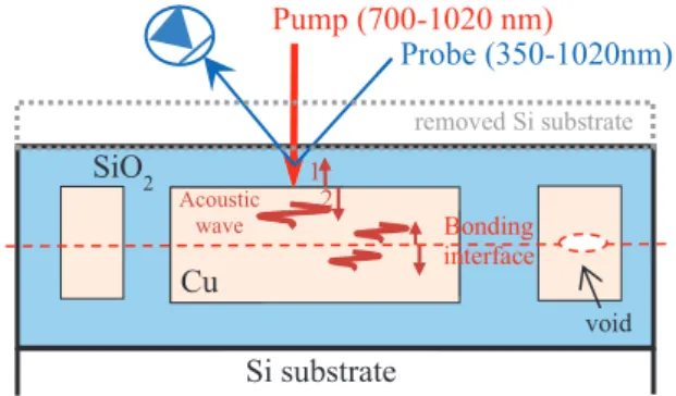
Picosecond acoustics [5] is an optical technique that uses a femtosecond laser in a pump-probe configuration to generate and detect acoustics at ultra-high frequency. The pump laser beam generates acoustic waves which propagate through the sample. The probe laser beam detects the acoustic waves back to the surface after reflection on the different interfaces (Fig. 1). This technique is using acoustics like the SAM but at much
higher frequencies (10-300 GHz) that makes the in-depth resolution much higher.
APiC is a variant of picosecond acoustics that takes advantage of tuning the laser wavelength to offer more capabilities[6]. For example, choosing the wavelength, let follow the acoustic pulse propagation inside the studied stack, giving more information about it [7].
Figure 1. Acoustic generation, propagation and detection on
the studied stack.
3. STUDIED SAMPLE
This study is made on a stack composed by two wafers bonded face to face. The Si substrate of top wafer has been removed. The interface between the two bonded wafers is composed of bonded copper pads and lines (4 to 7 μm wide) separated by silicon di-oxide. A silicon oxide layer is present above the copper lines (Fig. 1). SAM images focused on the bonding interface reveals the presence of defects in the vicinity of some copper lines, especially at the wafer edge (Fig. 2). The present study is focused on these copper lines.
The different image contrasts are found linked to the Cu lines width (Fig. 2) or to the void concentration in Cu bonded lines. The black areas are bonded lines and pads with no defect or void width inferior to SAM resolution.
Figure 2. Scheme of Cu lines position and width on a wafer
edge (left) and SAM image focused on hybrid bonding interface showing different contrasts revealing the influence of Cu lines width on defects occurrence (right). The red crosses represent the location of APIC measurements.
Cu lines w=7μm Cu lines w=4μm Cu lines w=1μm Staggered Cu lines w=2μm Wafer edge Probe (350-1020nm) Pump (700-1020 nm) SiO2 Si substrate 2 Acoustic wave Cu 1 2 Bonding interface void removed Si substrate x x
4. APIC MEASUREMENTS
APiC is performed on the sample at various locations of the wafer edge that have revealed different SAM contrasts. (Fig. 2). Acoustic wave is generated at copper level and propagates into SiO2 toward the surface (wave n°1 in Fig. 1) and into Cu toward the bottom of the sample (wave n°2 in Fig. 1). Figure 3a shows APiC signal on wafer location with black (black plot) and white (red plot) SAM areas: after the fast response (0 ps), Brillouin oscillations [7] are seeable, acousto-optic signature of the SiO2 wave n°1 is going through. At 100 ps, a first step [8] corresponds to this acoustic wave reaching the surface. Meanwhile, wave n°2 is partially reflected by the bonding interface and reaches the surface at 280 ps, showing a smaller step on the signal.
The plots show a large difference between APiC signal amplitude ratio obtained on black and white SAM areas at 280 ps (black frame in Fig 3a). That suggests that the variation of the step amplitude is related to the interface quality: when there is no defect at the interface, the interface is almost transparent for acoustic waves. The waves are very lightly reflected at bonding copper interface and mainly keep going through underneath copper. They are reflected at the bottom of the copper layer then come back to the surface. However when a defect is present at the bonding interface, a larger part or even the totality of the acoustic waves is reflected on the defect and comes back to the surface at an earlier delay.
0 100 200 300 400 500 600
280 ps
'
R/R (arb.unit.)
Time (ps)
signal on black area signal on white area
100 ps 0 0 20 40 60 80 100 2 4 6 8 10 12 14 16 18 20 22 24 white 280 ps step amplitude SAM grayscale black
Figure 3. a) APIC Signal on white area (red plot) and on black
SAM area (black plot). b) 280 ps step amplitude measured on black (red dots) and white (black dots) area on SAM image compared to grayscale level extracted from SAM image on the studied areas (red crosses in Fig 2)
Following this assumption, it can be deduced that signal on a defect free area would only shows a small step at 280 ps while signal on an area with a void would show a step with higher amplitude. Signal on white area from Fig 3a shows a 280 ps step amplitude 20 times higher than on black area signal. This shows a consistency between SAM and APiC measurements.
5. APIC VS SAM
The amplitude of the 280 ps step can be extracted for a quantified study of the black and white areas and comparison with SAM technique.
APiC measurement is repeated at various points of each area (with black and white SAM contrasts) to get statistics. After a normalization of the signals to make them comparable to each other, the 280 ps amplitude is extracted from each signal. Theses value are high for white SAM area (between 7 and 23) and low for black
area (between 0 and 1,5). Grayscale level are extracted from SAM images on both studied areas with an image editor software in order to get a quantified value for comparison with 280 ps step amplitude. On white area, the greyscale level is 99,4 and on black area it is 0,5. The comparison between APiC 280 ps step amplitude and SAM grayscale level (Figure 3b) is consistent. However, 280 ps step amplitude on wafer areas with SAM white contrast covers a large amplitude range (7-23) while SAM grayscale stays constant at 99,4. This can be explained by APiC spatial resolution (1-2 μm) compared to SAM resolution (20 μm). We make the hypothesis that the areas with SAM white contrasts are not uniform in terms of void density. SAM gives a mean response of the voids, getting a uniform value while APiC that is much more local would detect voids with width within the laser spot resolution. TEM observation on black and white area would confirm the presence and density of voids.
6. CONCLUSION AND PERSPECTIVES
APiC measurements were performed on Cu/Cu lines bonded by hybrid bonding stacking. A correlation is found between the contrasts on SAM images and amplitude variation of a specific contribution on APIC signals. We have demonstrated that the higher spatial resolution of APIC technique could lead to a more accurate localization of the defects. This work would be to extend the study to grey areas where the density of void should be different than on white areas.
7. REFERENCES
[1] “2.5D / 3D TSV & Wafer-Level Stacking: Technology & Market Updates report”, 2019 edition - Yole Développement
[2] "Reliable 300 mm wafer level hybrid bonding for 3D stacked CMOS image sensors", S Lhostis et al., 2016 IEEE 66th ECTC
[3] “The Scaling of Cu-Cu Hybrid Bonding For High Density 3D Chip Stacking.” Y. Kagawa et al., 2019 EDTM 297-299.
[4] "Non-destructive wafer-level bond defect identification by scanning acoustic microscopy", S. Brand et al., Microsyst Technol (2015) 21: 1385. [5] "Surface Generation and Detection of Phonons by
Picosecond Light Pulses", C. Thomsen et al., Phys. Rev. B. 34, 4129 (1986).
[6] “Colored ultrafast acoustics: From fundamentals to applications”, A. Devos, Ultrasonics, 56, 90-97 (2015). [7] “A different way of performing picosecond ultrasonic measurements in thin transparent films based on laser-wavelength effects”, A. Devos et al., Appl. Phys. Lett., 86, pp.211903 (2005)
[8] “High-laser-wavelength sensitivity of the picosecond ultrasonic response in transparent thin films”, A. Devos et al, Phys. Rev. B. 74. 64114-. 10.1103 (2006)
a) b)