CHARACTERIZATION AND MODELING OF SMALL
AREA Hgl_,CdTe PHOTODIODE SPATIAL RESPONSE
by
Gary James Tarnowski
Submitted to the Department of Electrical Engineering and Computer Science
in partial fulfillment of the requirements for the degrees of
Master of Science in Electrical Engineering
and
Bachelor of Science in Electrical Engineering
at the
MASSACHUSETTS INSTITUTE OF TECHNOLOGY
May 1993
@
Gary James Tarnowski, MCMXCIII. All rights reserved.
The author hereby grants to MIT permission to reproduce and to distribute copies
of this thesis document in whole or in part, and to grant others the right to do so.
Author
.,,Department of lectr al Engineering and Computer Science
May 18, 1993
Certified by
.
..
Clifton G. Fonstad
rofessor of Electrical Engineering
Thesis Supervisor
Certified byMargaret H. Weiler
Staff
gineer, Loral Infr
~maging
Systems
72
.Thesis
Supervisor
Accepted
//MASSACHUSETTS
INSTI•rTE
~f
9L.R
A R''I;
...
!'RRE
CHARACTERIZATION AND MODELING OF SMALL AREA
Hgl_,CdTe PHOTODIODE SPATIAL RESPONSE
by
Gary James Tarnowski
Submitted to the Department of Electrical Engineering and Computer Science on May 18, 1993, in partial fulfillment of the
requirements for the degrees of Master of Science in Electrical Engineering
and
Bachelor of Science in Electrical Engineering
Abstract
This thesis is concerned with three-dimensional numerical modeling and blackbody slit scanner test-ing of the direct space and frequency domain spatial responses of small area, backside illuminated, long wavelength infrared, heterojunction Hgl_,CdTe photodiodes. The simulation helped to iden-tify factors by which single-pixel modulation transfer function (MTF) might be improved, and an example of that improvement is included. Single pixel MTF was also shown to be dominated by the detector pixel pitch and relatively independent of pitch/mesa ratio. The numerical model was compared to an analytical model, with the results in good qualitative agreement. A blackbody slit scan test and analysis methodology was developed. Slit scans were taken and analyzed on represen-tative small area photodiodes, and the results compared to the numerical model. When the optical input was deconvolved from the raw data, the apparent spatial definition was improved, but the deconvolution method introduced unphysical ripples into the deconvolved data.
Thesis Supervisor: Clifton G. Fonstad Title: Professor of Electrical Engineering Thesis Supervisor: Margaret H. Weiler
Acknowledgements
I wish to thank Professor Clifton Fonstad for his role as my on campus advisor for this thesis. In particular, I thank him for his criticism despite the short time frame and for a useful discussion
regarding the simulation symmetry and boundary conditions.
Many people were helpful at Loral Infrared and Imaging Systems, the supporters of this research. First and foremost, I express my gratitude to Dr. Margaret Weliler, my company advisor. No matter the adversity, she could conjure a solution. Her supervision of this project, critical readings of this thesis, and generous donation of her time are greatly appreciated.
I thank Nancy Hartle, supervisor of Device Design and Test, for running hurdles which I have not encountered thanks to her. Her more global viewpoint of this project and its motivation was valuable. Dr. Ronald Briggs is thanked for our discussions, as well as for his original creation of the cylindrical coordinates code. I am also grateful for his procurement of hardware for this project, as well as for his thoughtful original design of the spot scan station. I thank Dr. Kevin Maschhoff for our discussions on the MTF of most everything and for his clarification of points. Lynne Tersis is noted for concurrent work on deconvolving the spot and for originally exploring some of the test analysis issues. Richard Hassler, of Optical Engineering, is thanked for the generation of polychromatic objective MTFs. I am grateful to Robert Minich, head technician, for putting up with a host of questions and for scheduling the testing in. I also thank Karl Gustavsen for his showing me the ropes on the spot scan station. Finally, I'd like to thank Steve Krusemark for putting up with integrals and worse, and for knowing so much about bicycling.
More generally, this document represents the culmination of much of my MIT experience. I sincerely thank my parents for their love and support during these five years, and particularly during the adversities of this term. Now that I am a smidgen older, I realize what exceptional people they are.
I also wish to thank my friends here, whom I always wish good luck. I thank my present roommate Matt Bloom for his good humor as we sailed our similar boats this year. I'm grateful to that influential group who've been through a great deal: Cam Daly, Steve Janselewitz, Brian Elder and Ed Walters. I certainly thank Antoinette Baker for her uncomplaining receipt of many tidings, and for her taste in geometric forms. Finally, I thank Banu Ramachandran for her patience, grace, and extraordinary kindness during much of my time here. Thank you, everyone, and best wishes.
Contents
1 Introduction 13
1.1 Background ... ... ... . .... ... .. 13
1.2 Imaging System MTF ... ... 15
1.3 O utline . . . .. 16
2 Photodiode spatial response theory 17 2.1 MTF models of the sampled imaging system .. . . . . 17
2.2 Analytical models of single pixels ... 19
2.2.1 Convenient models ... . 19
2.2.2 Cheung's m odel ... ... .. 21
3 Numerical modeling 23 3.1 Derivation of the numerical model . . . . ... . . . . .. . . . . 23
3.1.1 Physical assumptions ... ... ... ... ... .. 23
3.1.2 Mathematical assumptions ... ... ... 25
3.1.3 Discretization . . . .. .. . 29
3.2 Use of the numerical model ... 31
3.2.1 Provisions . . . .. . . . 31
3.2.2 Verification .. ... ... ... ... .. 32
3.2.3 Operational constraints ... 32
3.3 Results for a symmetric staring array . ... . . . . 35
3.3.1 Standard case MTF(f,,f,) ... 35
3.3.2 Parameter variations ... 47
3.3.3 Discussion ... .. ... ... ... 57
3.4 Optimization example ... ... 61
4 Characterization Theory 73 4.1 The test as an LSI system ... . 73
4.2 Test geometry . .
4.3 Optical input . . ... .... ... .... .... ... .... ... .... ... ... 75
4.4 Exam ple output ... 77
5 Application of the test model 78 5.1 Uncertainty (Signal-to-noise ratios) ... 78
5.1.1 The optical input ... ... .. 78
5.1.2 The electronics at system output . ... . . . . 82
5.2 Optimizing the test procedure ... 86
5.2.1 Optimizing the optical input ... 90
5.2.2 Optimizing to reduce random noise ... 91
5.2.3 Optimizing the discretization ... 91
6 Test results and analysis 92 6.1 Results of scanning the Small Staring Array . ... . . . . 92
6.2 Comparison of results with slit and step size trades . ... 98
6.2.1 Step size . ... ... . 98
6.2.2 Slit size . ... .... ... .... .... ... .... ... .... ... .. 103
6.3 Results of scanning the Small Scanning Array . ... . . . 108
6.4 Comparison of results with the numerical model . ... . 117
7 Conclusions 121 7.1 Summary and Evaluation ... ... 121
7.1.1 M odeling . . . 121
7.1.2 Testing . . . .... . . . .. . . 122
List of Figures
1-1 Schematic of a typical infrared imaging system. After reference [4]. . ... . 14 1-2 Schematic of a focal plane array, the element of the IIS examined in this research. Such
arrays are constructed by replicating individual photodiodes, also shown in schematic. 14 2-1 The diode geometry, sampling grid, and pitch. Solid lines indicate the array of
photo-diodes. The interior squares are the physical junctions, and the larger outer squares define the cell size. The sampling grid referred to in the text is given by the intersec-tion of the dotted lines. The respective pitches are also shown. . ... . 18 2-2 Modeling crosstalk between nearest neighbor diodes. Uniform collection of radiation
in central shaded cell is assumed. ... ... . . 20 2-3 Cheung PV detector array MTF model. The carrier diffusion MTF(f) is the curve
which is everywhere non-zero. The pitch sinc(irwf) is the middle curve at f = 20 cycles/mm, going to zero at (1000 / 35) cycles/mm. Their product, the detector MTF, is the lowest curve. These curves are shown for an absorption coefficient of 2000/cm, a base thickness of 15
pm,
a diffusion length of 15 itm, no collection enhancing field, and a detector pitch of 35 m. ... . ... . . 22 3-1 Symmetrically placed impulses force symmetric carrier and current densitydistribu-tions. The zy origin is at the center of the junction. . ... 26 3-2 The simulation domain in cross section and top view. The top view shows the quarter
of the full 7 by 7 pixel region over which the calculation takes place. Reflecting boundaries (mirrors) occur on the XZ and YZ origin planes. On the fourth pixel, in either x or y, the domain is terminated by a neutral boundary condition surface. The passivation and substrate recombination velocities may be independently allocated. All junctions are grounded so that the excess carrier concentration is zero. ... . 28 3-3 Flood illumination quantum efficiency variation with u grid size. The quantum
effi-ciency is expected to converge to a single value as the grid size tends to infinity. All error terms in the Taylor series expansions vanish in that limit. . ... 33
3-4 Diode impulse response, dir(0, 0), quantum efficiency variation with u grid size. The quantum efficiency is expected to converge to a single value as the grid size tends to infinity. All error terms in the Taylor series expansions vanish in that limit . . . . . 34
3-5 Schematic of the Small Staring Array 35 pm sparse geometry . . . . . 35
3-6 Small Staring Array simulation. The diode slit response(z) is the normalized collected
photocurrent versus location of an infinitesimally thin slit of LWIR illumination. Its transform is the z direction profile MTF of the diode. . ... 37 3-7 Small Staring Array simulation. The Diode Slit Response(f.) is the profile MTF of
the diode in the z direction ... 38 3-8 Small Staring Array simulation. Diode slit response(y). Here the slit is scanned
across the y direction. Since this array is symmetric in
a
and y, the responses for both directions are the same. ... 39 3-9 Small Staring Array simulation. Diode Slit Response(fy), the profile MTF in the ydirection, which is by symmetry the same as that in the a direction . . . . . . 40
3-10 Small Staring Array simulation. The diode impulse response(z, 0) is the normalized
collected photocurrent versus location of an infinitesimally small spot of LWIR illu-mination. Here the response is shown versus the location of this spot along the z axis. This corresponds to a "perfect" spot scan in . . . . 41
3-11 Small Staring Array simulation. Diode impulse response(0, y). Here the response to
a infinitesimal spot is shown versus spot location along the y axis. This corresponds to a "perfect" spot scan in y ... 42
3-12 Small Staring Array simulation. The diode impulse response(z, y) is the full scan of
the diode in z and y by an infinitesimally small spot . . . . 43
3-13 Small Staring Array simulation. The Diode Impulse Response(f., 0) is the f, axis
profile slice through the full two-dimensional MTF. It is equivalent to the transform of the slit response ... .... ... .... .... ... .... . .. . ... ... ... 44 3-14 Small Staring Array simulation. The Diode Impulse Response(0, fy) is the f~ axis
profile slice through the full two-dimensional MTF. It is equivalent to the transform of the slit response ... ... . ... . 45
3-15 Small Staring Array simulation. The Diode Impulse Response(f., fy) is the
normal-ized Fourier transform of the dir(z, y). This is the full two-dimensional MTF of the diode. .. . . . .. ... .. . . . ... . . . . . . . .. . 46
3-16 Small Staring Array simulation. varying the absorption coefficient. Upper curve, c
= 2000/cm; Middle, 5000/cm; Lower, 10000/cm. The lower coefficient allows photo-generation closer to the junction, thus increasing MTF . . . . . 48
3-17 Small Staring Array simulation, varying the diffusion length. Upper curve, 1p = 15
Jpm; Middle = 20; Lower = 25. Increased diffusion length allows carriers to diffuse to
other cells, thus degrading MTF. ... 49
3-18 Small Staring Array simulation, varying the collection enhancing field. Upper curve,
Ez = 24 V/cm; Middle, 16; Lower, 8. The field forces the carriers toward the junctions,
increasing M TF. ... ... 50 3-19 Small Staring Array simulation, varying the surface recombination velocity. Upper
curve, a = 1000 cm/s; Middle, 100 cm/s; Lower, 0 cm/s. Increased velocities tend to
shrink the width of the diffusion point spread function, thus increasing MTF. ... 51 3-20 Small Staring Array simulation, varying the base layer thickness. Upper curve, Base
thickness = 12 Jim; Middle, 15; Lower, 20. The thin base layers increase MTF by bringing the junctions closer to the photogeneration. . ... . 52 3-21 Small Staring Array simulation, varying the mesa cut depth. Upper curve, Cut depth
= 7 jm; Middle, 5; Lower, 3. As the cut depth is increased, junctions become more spatially isolated, increasing MTF. ... 53 3-22 Small Staring Array simulation, 20 Jpm pitch, varying the pitch/mesa ratio. At the
array Nyquist frequency of 25 cycles/mm: Upper curve, Mesa of 16 Jim; Middle, 20; Lower, 10. Discussed in text. ... 54
3-23 Small Staring Array simulation, 25 Jim pitch, varying the pitch/mesa ratio. At the
array Nyquist frequency of 20 cycles/mm: Upper curve, Mesa of 20 Jm; Middle, 25; Lower, 16. Discussed in text. ... 55
3-24 Small Staring Array simulation, 35 jim pitch, varying the pitch/mesa ratio. At 12 cycles/mm: Upper curve, Mesa of 25 jim; Middle, 35; Lower, 20. Discussed in text.. 56 3-25 Small Staring Array simulation, 20 jim pitch. Upper curve, simulation, includes
8 V/cm drift field; Lower curve, Cheung model, without field. Simulation nearly
matches the analytical case ... 58 3-26 Small Staring Array simulation, 25 jim pitch. Upper curve, simulation, includes
8 V/cm drift field; Lower curve, Cheung model, without field. Simulation nearly
matches the analytical case ... 59 3-27 Small Staring Array simulation, 35 jim pitch. Upper curve, simulation, includes
8 V/cm drift field; Lower curve, Cheung model, without field. Simulation nearly
matches the analytical case ... 60 3-28 Cross sections of Small Scanning Array geometries, as input to the simulation, before
and after optimization. Only half of the center diode (c) is shown in each view. Nearest neighbor is indicated by (nn). All dimensions in pm. . ... . . 61
3-29 Small Scanning Array simulation, showing improvement of z direction slit response.
Upper curve, original dsr(z); Lower curve, optimized dsr(z). . ... 63 3-30 Small Scanning Array simulation, showing improvement of 0 direction profile MTF.
Upper curve, optimized DSR(f.); Lower curve, original DSR(f,). . ... . 64
3-31 Small scanning array simulation, showing improvement of y direction slit response.
Upper curve, original dsr(y); Lower curve, optimized dsr(y). . ... 65 3-32 Small Scanning Array simulation, showing improvement of y direction MTF. Upper
curve, optimized DSR(f,); Lower curve, original DSR(f,). . ... 66 3-33 Small Scanning Array simulation, showing improvement of z direction spot scan
re-sponse. Upper curve, original dir(z, 0); Lower curve, optimized dir(z, 0). ... 67
3-34 Small Scanning Array simulation, showing improvement in y direction spot scan re-sponse. Upper curve, original dir(0, y); Lower curve, optimized dir(0, y). ... 68 3-35 Small Scanning Array simulation showing original dir(z, y), or infinitesimal spot scan
response. ... .... .. 69
3-36 Small Scanning Array simulation, showing optimized dir(z, y). . ... 70
3-37 Small Scanning Array simulation, showing original DIR(f0, f,), or full two-dimensional
diode M TF . ... ... ... 71
3-38 Small Scanning Array simulation, showing optimized DIR(f., fV), or new full
two-dimensional MTF. ... .. 72
4-1 Spot/Slit scanner optical schematic, indicating all major optical elements of the scanner. 74 4-2 Code V polychromatic diffraction MTF for the optical system, and geometric aperture
MTF of the 10 pm slit. The diffraction MTF is physically cut off beyond 70 cycles/mm. 76 4-3 Small Staring Array diode slit response data. . . . .. . . ... . . 77 5-1 Code V polychromatic diffraction MTFs for the optical system. Upper curve, at
focus; middle curve, defocused 25
pm;
lower curve, defocused 50 im. The quality of MTF decreases with defocus. ... 795-2 Line of sight jitter MTFs, modeling lateral uncertainty. Upper curve,
a
= 0.5 pm;lower curve,
a
= 2pm.
MTF decreases with increasing jitter. . ... . . . . 81 5-3 Spot scan signal acquisition path. Each component potentially introduces orsup-presses noise. .. ... .... ... .... .... ... ... ... .... ... . 82
5-4 Analytic (solid line) and discrete (dotted line) Fourier transforms of a 36 pm wide rect function. The discrete data is on 4 pm steps, and becomes higher than the analytic transform due to aliasing ... 84
5-5 Analytic (solid line) and discrete (dotted line) Fourier transforms of a 36 Jm wide rect function. The discrete data is on 2
pm
steps, and becomes higher than the analytic transform due to aliasing. ... ... 85 5-6 Analytic Fourier transform of a 36 jim wide rect function, solid line. Discretede-convolved transform, dotted line, has been corrupted by defocus, jitter, and aliasing, lowering the MTF. 2 ptm steps were used . . . . .... ... ... 87 5-7 Percentage of MTF lost in that point as a function of spatial frequency. This shows
by what percentage of its value each point is low. ... . 88 5-8 Reverse transform of the truncated and corrupted MTF (points), shown with an ideal
36
pim
rect function. ... ... 896-1 Transform of raw Small Scanning Array slit scan response, lowest curve, transform of deconvolved data, middle curve, and transform of 35 jpm aperture, highest curve. The removal of the spot increases the MTF over the transform of the raw data. An aperture function continues to have content at high spatial frequency, since diffusion is not considered ... ... ... .. 94 6-2 Transform of raw data, lowest curve, transform of deconvolved data, middle curve,
and transform of 35 pim aperture, highest curve. This is the result of Figure 6-1, plotted out to the array sampling frequency. ... .... 95 6-3 Raw slit scan data, upper curve; deconvolved data, lower curve. While the central lobe
is made considerably more narrow, many ripples are introduced which are particularly visible on a logarithmic scale. . ... ... ... . . 96 6-4 Raw data, upper curve; deconvolved data, lower curve. This is the data of Figure 6-3
on a linear scale, so the ripples are less visible. . ... .. 97 6-5 Deconvolved MTF for the 2 pm and 4 pm step size. 2 /Am step size peaks slightly
around 62 cycles/mm. Either step size should prove acceptable. . ... . 99 6-6 Deconvolved MTF for the 2 jpm and 4 pm step size, showing negligible difference in
the region extending to the array sampling frequency. . ... 100 6-7 Deconvolved diode slit responses for 2 and 4 jpm step sizes. Both are aggravated by
ripples but the 2 pm scan has a lower average value at large distances from the origin. 101 6-8 Deconvolved diode slit responses for 2 and 4 jpm step sizes. The 2 jpm scan is off center. 102 6--9 Deconvolved MTF curves for the 10 jpm and 20 jtm slit size, showing negligible difference. 104 6-10 Deconvolved MTF curves for the 10 jim and 20 pm slit size, showing negligible
dif-ference out to the array sampling frequency. ... .... 105 6-11 Deconvolved diode slit responses for 10 and 20 im slit sizes. The ripple problem
6-12 Deconvolved diode slit responses for 10 and 20 jpm slit sizes. The 20 tpm slit scan is off center, but the shape of the central lobe appears to match well. . ... . 107 6-13 Transform of raw slit scan response for the narrow direction of the Small Scanning
Ar-ray, lowest curve, transform of deconvolved slit response, middle curve, and transform of 50.8 •,m aperture, highest curve. ... ... 109 6-14 Transform of raw slit scan response, lowest curve, transform of deconvolved slit
re-sponse, middle curve, and transform of 50.8 lim aperture, highest curve. This is just the data of Figure 6-13 plotted out to the array sampling frequency. . ... . 110 6-15 Raw slit scan response, upper curve; deconvolved slit response, lower curve. While
ripples are evident, the deconvolved response is everywhere lower than the raw data. 111 6-16 The data of Figure 6-15 on a linear scale. Raw data, upper curve; deconvolved data,
lower curve. Deconvolution removes the width of the spot. . ... . 112 6-17 Transform of raw slit scan response for the wide direction of the Small Scanning Array,
lowest curve, transform of deconvolved slit response, middle curve, and transform of 50.8 pim aperture, highest curve. ... ... 113 6-18 Transform of raw slit scan response, lowest curve, transform of deconvolved slit
re-sponse, middle curve, and transform of 50.8 pm aperture, highest curve. This is just the data of Figure 6-17 plotted out to the array sampling frequency. . ... . 114 6-19 Raw slit scan response, upper curve; deconvolved slit response, lower curve. Ripples
are evident, and the deconvolved response is not everywhere lower than the raw data. 115 6-20 The data of Figure 6-19 on a linear scale. Raw data, upper curve; deconvolved data,
lower curve. Deconvolution removes the width of the spot. The response is seen to be asymmetric. . . . . . ... ... . . . 116 6-21 Deconvolved DSR of data for the Small Staring Array, lower curve. DSR yielded from
numerical model, upper curve. ... ... . . 118 6-22 Deconvolved DSR(f,) of data from the Small Scanning Array, lower curve. DSR
yielded from numerical model, upper curve. . ... .... .. j119 6-23 Deconvolved DSR(fv) of data from the Small Scanning Array, lower curve. DSR
List of Tables
Chapter 1
Introduction
1.1
Background
High performance infrared imaging systems (IIS), as pictured in Figure 1-1, find applications in thermography, night vision, search and rescue operations, atmospheric spectroscopy, military recon-naissance, surveillance, target acquisition and tracking. Increasing system performance demands better individual system components. In particular, requirements which focus on the relation be-tween the contrast in some radiant object and the contrast in its corresponding image are of interest. This relation can be formalized by the modulation transfer function (MTF) of the system. Assumn-ing some imagAssumn-ing system is linear and spatially shift invariant (LSI), the usual Fourier transform techniques are applicable and the transfer function indicates how well the IIS preserves contrast in the image as detail increases in the input illumination scene. The focal plane array (FPA), shown schematically in Figure 1-2, is the transducer from photons to electrons, and allows the optical sys-tem to interface 'with the electronic syssys-tems which follow it. The drive to make syssys-tems not only better at imaging, but lower in total size, weight, thermal load, and power dissipation concentrates attention on improving the MTF performance of these arrays.
Linear or square FPAs are made of single photodiodes, also shown in Figure 1-2. Linear scan-ning arrays may have 4 x 480 elements and square staring arrays may have 256 x 256 elements. Staring arrays are of particular concern since their use can eliminate mechanical moving parts like scanning mirrors, thereby reducing system size, weight, and complexity. This thesis focuses on long wavelength infrared (LWIR) liquid-phase epitaxially grown (LPE) P-on-N Hgl_,Cd,Te hetero-junction photodiodes, such as are fabricated at Loral Infrared and Imaging Systems (LIRIS), where this research was performed. Their spatial response may be characterized by the diode impulse response function, dir(z, y), or equivalently in the spatial frequency domain by its Fourier
trans-Target . Backgound Window Optics Filter Effective Eye play Detector array
Figure 1-1: Schematic of a typical infrared imaging system. After reference [4].
FPA
Single photodiode and neighbors
hf
L
1mrnrT rFLi r
4 video lines Si readout
electronics
hf
A/R coating
CdTe substrate
thin n-HgCdTe base layerp-HgCdTe cap layer
In bump
Interconnects
Figure 1-2: Schematic of a focal plane array, the element of the IIS examined in this research. Such arrays are constructed by replicating individual photodiodes, also shown in schematic.
form, DIR(fe, fy)', where the spatial impulse is an infinitesimally thin bandlimited "ray" from a blackbody source whose photon flux density is such that low level injection conditions prevail in the diode. It is this DIR(f., f,) which is the single pixel MTF.
The MTF is of concern in both thermal imaging system design, since one wants to predict sys-tem performance, and in IIS evaluation in order to prove that the syssys-tem performs as expected. The designer needs to be aware of the trade-offs between increasing MTF at the expense of other measures of IIS performance. In direct-space, the principal trade-off is between the flood illumina-tion response of a photodiode and the response as a funcillumina-tion of illuminaillumina-tion impulse distance from the diode. The mesa and junction areas of such photodiodes are generally made smaller than the "cell" size of the diode in order to reduce space charge region generation-recombination currents and junction perimeter leakage currents [8], as well as the gamma-ray sensitive area [9]. Thus the diode photocurrent strongly depends on lateral optical collection in order to enhance the effective quantum efficiency. However, as device dimensions approach that of a diffusion length, carriers photogenerated in one cell may be collected by the junction of some neighboring cell, compromising the spatial definition of the array's pixels. Similarly, trade-offs between MTF and noise levels may be found.
1.2
Imaging System MTF
Any intensity pattern may be constructed by the appropriate sum of sinusoidal waveforms. Thus any object intensity may be Fourier transformed. First, a simple sinusoidal incident illumination intensity is considered:
i(z) = Ade + A.c cos 2Afz (1.1)
The modulation in such a waveform is given by
Ae
M Aac (1.2)
Ade The modulation transfer function is then just
MTF = Mimage (1.3) Mobject
Since the system output, or image, is likewise transformable, there exists a system function
MTF(f) - Mimage(f) = Aimage,ae(f) (1.4)
Mobject(f) Aobject,ac(f)
1
and it may be seen that the MTF(f = 0) is always equal to unity; that is, the dc input suffers no modulation, although it is generally scaled from subsystem to subsystem. The transfer function of an entire imaging system might be modeled [6] as
MTF(f) = MTFLos MTFOPTMTFARRMTFELC MTFDSP MTFEYE (1.5)
with the subscripts indicating the MTF associated with
LOS Line of sight jitter (mechanical instability) OPT Optics
ARR Focal plane array and readout electronics
ELC Electronics,, including A/D converters, filters, and amplifiers
DSP Display (like a CRT)
EYE Effective eye, or just the eye for a human observer
The MTF of the detector array alone, as given in [6] is the product of the detector size and detector spacing MTFs, both of which are given as sinc functions of the appropriate widths. If array MTF is improved, either the whole system MTF may be improved or the requirements on some other portion of the system may be made less stringent, potentially reducing costs. The MTF model described above, while convenient, does not deal with detector MTF in detail. More detailed models of diode MTF, including carrier diffusion, follow.
1.3
Outline
This thesis begins with the theory of photodiode and FPA spatial response, examining the effects of carrier diffusion, photodiode geometry, sampled-scene phase, sampling and aliasing in Chapter 2. Chapter 3 describes the implementation and results of a three-dimensional numerical model whose outputs are the direct and frequency space responses of simulated photodiodes. The results are used to show how an FPA may be designed to optimize its single pixel MTF performance. Chapter 4 describes blackbody slit scanner testing of photodiodes, again from a transfer function point of view. This allows the removal of the effects of a finitely-small input illumination form. Chapter 5 discusses the real-world application of this test model, given signal-to-noise and other uncertainty issues. Chapter 6 presents results of the slit scans in both the direct and frequency space domains, before and after deconvolution of the slit and optical diffraction patterns. Finally, results are summarized and assessed in Chapter 7, and suggestions for future efforts are made.
Chapter 2
Photodiode spatial response
theory
The spatial response problem can be examined in terms of the whole array or in terms of just a single diode. This chapter first discusses attempts to specify the MTF of the shift variant FPA, and then examines modeling the spatial response of just a single detector.
2.1
MTF models of the sampled imaging system
The imaging system cascade models presume both linearity and shift-invariance. Although linearity shall be assumed hereafter, nonlinear responses and nonuniform responses of any part of these systems makes their description difficult and degrades their performance. Several issues must be dealt with in modeling the FPA. Incident illumination is converted from some analog waveform into a spatially discrete representation. The response of any photodiode to illumination depends on the the phase of the illumination with respect to the sampling grid, and is therefore shift-variant. This grid is given by the center-to-center spacing between the detectors. The center-to-center spacing is called the pitch and can in general be different for both z and y. This is illustrated in Figure 2-1. Since a sampling process is involved, the spectrum of the output is aliased about the sampling frequency. While the problem of aliasing can be avoided by low-pass filtering the input waveform using the optical system, the sampling phase dependence cannot. Additionally, diffusion in the substrate needs to be addressed, no matter what geometry is proposed. While all these issues have not been dealt with by a single author, a review follows in order to show how each piece may be addressed.
The model of Wittenstein, et al. [11] neglects carrier diffusion, but is an excellent introduction to the issue, although its conclusion is not very useful. An analogy is drawn between isoplanatism
Vertical
PitchI
I
I
I
Horizontal PitchFigure 2-1: The diode geometry, sampling grid, and pitch. Solid lines indicate the array of photo-diodes. The interior squares are the physical junctions, and the larger outer squares define the cell size. The sampling grid referred to in the text is given by the intersection of the dotted lines. The respective pitches are also shown.
in direct space and isoplanatism in Fourier space. For optical systems, the direct space region where the system is shift invariant is the isoplanatic region, or corrected field. In the region where the MTF of the reconstructed and continuous function is not compromised due to phase, the region is deemed isoplanatic. The paper essentially extends the Nyquist criterion to optical systems and examines when it is adequate.
Park, et al. [7] take a somewhat more useful approach in that they determine a limiting case model which is the basis (or could be the basis) for the pitch MTF used in typical array MTF models. The approach is to assume the input functional phase is unknown, and to average the MTF over all possible locations relative to the sampling grid. This stochastic approach is equivalent to convolving the input function with the two-dimensional rectangle function associated with the pitch of the pixels. This approach provides a useful limiting case for design decisions, although taken alone it would indicate that maximizing the pixel density is all that is required.
de Luca, et al. [4] approaches the problem uniquely by not using Fourier techniques, but by finding the results in direct space. While representing pixels as uniform response apertures located on a certain pitch, and again neglecting diffusion, the MTF can be written down by integrating the incident sinusoid over the detector aperture while keeping track of its phase, and then finding those discrete pixel responses which are highest and lowest on the entire focal plane. Thus the MTF is found as a function of phase; furthermore the high point and low point are picked out for any frequency. Hence the issues of discrete outputs, sampling, aliasing, and phase are incorporated into the model. Only the single pixel response is simplified.
2.2
Analytical models of single pixels
2.2.1
Convenient models
The spatial response of single pixels is often grossly simplified for convenience. Gaussians may be used, based on fitting spot scan or slit scan data. Models may not include carrier diffusion at all, and assume a uniform response across the pixel aperture. Some models may acknowledge crosstalk, and use measured data to weight and then linearly superpose two aperture functions in direct space and thus two sinc functions in frequency space, as shown in Figure 2-2. Let the function rect(z/X) indicate a rectangle of unit height centered on the origin whose width is given by X. Its Fourier transform is denoted by the sinc function, or sin(frXf.)/(7rXf,). A real diode response, however, does not have step discontinuities like the rect function does.
Photodiode and nearest neighbors
O !I
n~~~
Relative response 100% 1%Figure 2-2: Modeling crosstalk between nearest neighbor diodes. Uniform collection of radiation in central shaded cell is assumed.
-do*-3
[7
2.2.2
Cheung's model
Cheung's model [3] bears the closest resemblance to a real diode response except for the numerical modeling in this thesis. The model assumes an array of junctions with no separation between junctions. Incident from the backside is a monochromatic sinusoidal input. The assumptions made and solution are very similar to the approach taken in Chapter 3. The drift/diffusion equation is solved for the charge concentration. The current density into the junctions is found as a function of a and
f,.
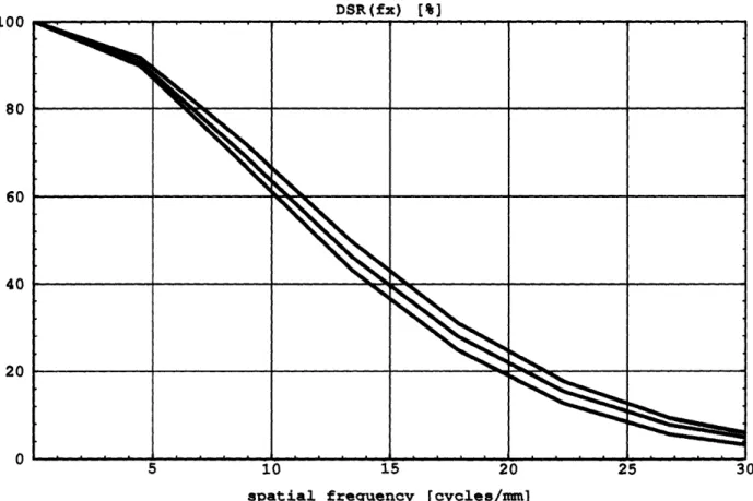
The quantum efficiency is then found as a function of sinusoidal illumination spatial frequency. Upon normalization to the dc quantum efficiency, the model yields the MTF due to carrier diffusion alone, or MTFcD(f). The integration over the depletion region is recognised to be a convolution of the current density with a rect function. Hence the complete MTF for this case may be written asMTF(f) = MTFCD(f)sinc(rwf) (2.1)
where w is both the width and the pitch. The result of this model is illustrated in Figure 2-3. This model solves for a one-dimensional MTF. In the case of LIRIS photodiodes, the mesa area is often less than the pitch area, as schematically shown in Figure 2-2. The diffusion point spread function is different for this geometry which includes spatially distinct junctions, mesa delineation cuts and frontside surface recombination. Since the point spread function is different, shift-variant, and not analytically tractable, the numerical model of Chapter 3 was implemented to correctly calculate the single pixel photoresponse, whose Fourier transform is the single pixel MTF, without resorting to undue simplification. Chapter 3 discusses how this single pixel MTF might be combined with the model given in [4] to yield a complete FPA MTF.
Cheung detector MTF model
40 spatial frequency [cycles/mm]
Figure 2-3: Cheung PV detector array MTF model. The carrier diffusion MTF(f) is the curve which is everywhere non-zero. The pitch sinc(rwf) is the middle curve at f = 20 cycles/mm, going to zero at (1000 / 35) cycles/mm. Their product, the detector MTF, is the lowest curve. These curves are shown for an absorption coefficient of 2000/cm, a base thickness of 15 Jim, a diffusion length of
15
pm,
no collection enhancing field, and a detector pitch of 35pm.
100
80
60 40 20 0 A ... -16Chapter 3
Numerical modeling
A desirable MTF model would incorporate the following effects: diffusion, array geometry, spa-tial phase, sampling, discretization and aliasing. Both Cheung's and de Luca's models use direct sinusoidal input to find an MTF. Instead of a simple uniform aperture, the integral in de Luca's expression for sampled modulation response (SMR) could be performed over the "real" spatial pro-file of the diode, the diode impulse response function. In particular, the product of an incident sinusoid and a numerically found diode impulse response could be integrated for several different phases and frequencies. The high and low valued pixels on the FPA could be found, generating a phase-dependent MTF. This MTF would characterize the shift-variant FPA. This chapter describes how the spatial profiles of single detectors may be found by a numerical model. The approach is that of [1, 2], where the calculation is here extended from cylindrical to rectangular coordinates.
3.1
Derivation of the numerical model
3.1.1
Physical assumptions
The complex physics of the p-n heterojunction requires simplification so that a tractable problem is posed and solved. The simulation domain is considered entirely within the n-type base of the detectors and concerns itself with excess minority carriers only. The assumptions include
* Negligible thermal gradients; thermal equilibrium between electrons and the lattice.
* Scalar dielectric constant E, and scalar hole mobility yp and diffusion coefficient Dp obeying the Einstein relation
(3.1)
Anp q
o The material is quasineutral so that
V
-
EE
=
p 2_ 0
(3.2)
* The electric field is curl-free, and there are no externally imposed magnetic fields
Vx E = 0
(3.3)
* Thus the electric field in the material is a constant, Ez, arising from the alloy composition gradient. It is assumed to be z-directed and collection enhancing.
* Boltzmann transport, so that the current density equation for holes may be written as
J, = qpppE - qDpVp (3.4) and the continuity equation may be written as
Op SGp- Rp- 11V Jp (3.5)
at q
where Gp is the generation rate for holes and Rp is the recombination rate. * Excitations and responses are static and fully time-independent.
* All radiation is monochromatic and normal to the substrate such that secondary reflections (optical crosstalk) are negligible. Further, the radiation is absorbed in the base layer and generates carriers at a rate of
G,(Y, y, z) = l(x, y)ae-az (3.6)
where ,(x, y) is the incident monochromatic photon flux per unit time per unit area, and a is a function of wavelength.
* The depletion approximation is employed.
* Defining the excess minority carrier concentration as
p' = Pn -
Pno
(3.7)
where pno is the thermal equilibrium concentration, low level injection (LLI) is assumed and the recombination is modeled as
where rp is the hole lifetime. The hole diffusion length is defined by the usual expression
1 P' D,p p pr
Analytic equations
Given the above assumptions, a single drift-diffusion equation may be carrier concentration
Gp(Z, y,
z)=
+ pPEz
-
DpV
2p'
which is valid in the bulk of the material.
Along the boundaries of the domain, the concentration and/or the must be specified. At any junction, under zero bias, in the depletion
p'
=
0
derived for the excess minority
(3.10)
derivative of the concentration approximation,
(3.11)
Along passivation surfaces, the surface recombination velocity s is introduced so that
Jh
=
qsp'
(3.12)where s is normal to the surface. The current elsewhere is given by Equation 3.4. In particular, the current into the center diode is of interest. Introducing zj to indicate points in z along the junction,
Jp=
I
z =
zi = qppp(zj)E. - qDp
-
Zx
1z= zr
(3.13)The photocurrent is then found by integrating J, (m, y, zj) over the central diode depletion region
surface
I =
tion J
(,
y, zj)dzdy
and the quantum efficiency is found by normalizing this current to the incident flux 4.
(3.14)
3.1.2
Mathematical assumptions
The simulation is necessarily over a finite point set, preferably as small as possible so that compu-tation times are short. Hence a symmetry argument is used to quarter the simulation domain, and artificial boundary conditions are used to bound the domain in z and y. Finally, the continuous solution, with these boundary conditions, is shown to exist and be unique.
x
III
Figure 3-1: Symmetrically placed impulses force symmetric carrier and current density distributions. The zy origin is at the center of the junction.
Symmetry and linear superposition
Consider four spatial impulses of monochromatic radiation each of intensity G placed symmetrically about the origin as shown in Figure 3-1. The impulses are shown on the frontside for visual clarity, but the following argument holds for backside illumination. No current due to just impulses I and II will flow across origin plane YZ; similarly for impulses III and IV. This is then true for the pairs of impulses (I, IV) and (II, III): the normal current flow through origin plane YZ is zero;
J(M = O, y, z) • , = 0 (3.15)
similarly for origin plane XZ.
There exists a certain minority carrier distribution throughout the material due to impulse I. The particular distribution is determined by the input, here G6(m - mo, y - Yo), the equations of the medium and the boundary conditions. If the charge distribution with only impulses I and II present is found, the current into the junction may be calculated. This current has a part due to impulse I and a part due to impulse II, and these parts are equal in magnitude. Similarly, when all four impulses are on, the current is just the sum of the four equal contributions. The solution to the medium's equation can also be determined by the boundary conditions. The carrier distribution in the presence of a reflecting boundary YZ is mathematically and physically indistinguishable from the distribution given the presence of a symmetrically located and symmetrically weighted impulse, as in the method of images often employed for electrostatic problems. Thus the response (the current)
due to the sum of the impulses is the same as the response due to one impulse with the symmetric boundary conditions at the XZ and YZ origin planes.
This introduces a new way to calculate the response to just one impulse. Employing the mirror boundaries, one may solve for the excess minority carrier concentration in just one quadrant. The distribution underneath the junction must be symmetric due to the symmetry of the excitation. Thus the distribution is known in all four quadrants. One then integrates J, over the entire junction area, and then recognizes that this solution is the same as that arising from four symmetrically placed inputs. By dividing the current by four, the response to a single impulse is found. Then, if the response of the system to all possible spatial impulses is calculated, linear superposition gives the response to any input form which is symmetric about both the XZ and YZ origin planes.
Artificial boundary conditions
Figure 3-2 schematically illustrates the simulation domain. Real boundaries, like the substrate and passivation are treated by use of a surface recombination velocity, where the mesa cuts are approxi-mated by perpendicular indentations. The mirror boundaries are one of the artificial boundaries, and are equivalent to surfaces with a recombination velocity of zero. The desired boundary conditions on the far edges would make the material seem forever continuous. Setting the carrier concentration to zero is not appropriate, since these walls are neither junctions nor Ohmic contacts. On the other extreme, reflecting boundaries would cause an abnormally high response (up to four times too large) due to impulsive illumination arriving near the edge, by the same arguments that drove the intro-duction of mirror boundary conditions. A so-called neutral boundary condition was chosen, where the boundaries are modeled as surfaces with s = Dp/lp to make them appear to be just more bulk
material. In practice, an accurate response was desired for illumination distances under the nearest and next-nearest neighbor; more pixels would have been added to the simulation domain in order to make the response insensitive to the recombination velocity chosen on this far boundary.
Existence and uniqueness of the solution
Equation 3.10 is a second-order partial differential equation. As such, it could be expressed as a Sturm-Liouville problem, whose solution is an infinite series of eigenfunctions. For a given set of boundary conditions involving a linear combination of p' and its first derivative, this series converges to a solution which both exists and is unique [5].
ve oasao VI Ur x-O ax bx ex ex mx s -Dp /Lp s of substrate s of passivation
Top View
p,-o
gy _ ey
by
/y
ay a = Dp/ Lp z Neutral boundaryi/
ax bx cx ex fx gx m x s = 0, mirrorFigure 3-2: The simulation domain in cross section and top view. The top view shows the quarter of the full 7 by 7 pixel region over which the calculation takes place. Reflecting boundaries (mirrors) occur on the XZ and YZ origin planes. On the fourth pixel, in either x or y, the domain is terminated
by a neutral boundary condition surface. The passivation and substrate recombination velocities
may be independently allocated. All junctions are grounded so that the excess carrier concentration is zero. z . zmax z - cut z-u -K s of passivation Cr,• S, ^;,
3.1.3
Discretization
Bulk equation
The equations are normalized for convenience. First, a normalized carrier concentration u is intro-duced
SDp' (3.16)
U---l-All lengths are also normalized to the diffusion length
lp.
Defining a parameter 3 = alp, a fullynormalized main equation may be written:
Ou
u = pe- z - 7dY + V'u (3.17)
where
- PEz (3.18)
kT
Standard finite difference techniques are used to discretize the equations on a uniform grid so that
Am = Ay = Az = A. For internal points, these approximations are used:
au
_ Uk+1 - Uk-1 + O(A2) (3.19)Oz 2A
&2u Uk+1 - 2u + Uk-1
=
2
+
O(2)
(3.20)
where subscripts are indicated only for those points where an index is changed from its default. Using i as the z index, j as the y index and k as the z index, this means that ui,j-1,k is written as just uj-l. The main equation may then be written in discretized terms.
A2/3e- -
az
A7"d,.(Uk+1 - uk-1) +i+ 1 + Ui- 1 + Uj 1 Ujl 1+ + 1.+l + Uk-1 + O(A4) (3.21) U =(6 + A
2)
Boundary conditionsIn general, the surface recombination velocity boundary conditions can be rewritten as
OIboundary (±- 7dt)IU (3.22)
where X indicates one of the three spatial dimensions, and the yd, is included if the boundary occurs in z and the signs are chosen based on the direction of s. The normalized surface recombination parameter is given by
, 5(3.23)=
The boundary condition in the case of mirrors is slightly simplified since, on the YZ mirror, for example, one may note directly that
= 0
(3.24)
892 2ui+1 - 2u
- + O(A 2) (3.25)
where in this instance i = 0.
These boundary conditions are typically introduced via the second derivative in this way
82u 1 7u
O2= - (-7u + 8u+i1 - Ui 2 - 6 A) + O(A2) (3.26)
or via the first derivative if appropriate
U- (-3ui + 4ui+l - ui+2) + O(A 2) (3.27)
Ox 2A
where these equations would treat derivatives at z = 0.
The boundaries can occur in either one, two, or three dimensions, so equations are combined where appropriate. A large fraction of the dif3d.c source code which implements the simulation is devoted to allocating the 192 special cases which result from the boundaries and the chosen geometry.
Error terms in the expansions
It may be shown that the main expression for u, Equation 3.21, and all other expressions on bound-aries are accurate to 0(A4 ) in the Taylor series expansion. From the carrier concentration u, the
current density is calculated via Ou/8z, which is only accurate to O(A 2). However, when the current
density is integrated over the junction area, a factor of A2 enters and the collected current has the form
I = Io + O(A4) (3.28)
where the subscript indicates the correct value. While this current has already been normalized to the flux, it remains to be normalized either to the diode area or the illuminated area. The area can only be specified to a precision of an integer multiple of A2. In the case of the diode impulse
response, or dir(z), the normalized illuminated area is just A2. Hence the final product, the quantum
efficiency, is only valid to
,q = 770 + O(A2) (3.29)
Typically the points are chosen to have a density of one point per micron in each dimension, so geometries can be laid out without ambiguity. The variation of efficiency with grid size is reported in Subsection 3.2.2.
Convergence and overrelaxation
Once the equations have been allocated to the grid points, the program simply steps through each point, doing the arithmetic. The new solution is emphasized over the old solution, however, as
follows
Unew = 1.93ujust calculated - Uprevious (3.30)
for each point. This is done to increase the rate of convergence of the u matrix with each iteration. The factor of 1.93 was empirically found to provide fastest convergence. When the sum of the absolute values of the difference between unew and Uprevious is less than a small number E,
E I(Unew - Uprevious)I < E (3.31)
whole grid
the solution is said to converge. The simulation has always converged in practice, except in an attempt to leave the "far" boundary conditions unspecified. The analogous continuous problem for that case is not guaranteed to have a solution.
3.2
Use of the numerical model
3.2.1
Provisions
The dif3d.c code provides for modeling rectangularly symmetric geometries and excitations. The user can simulate monochromatic flood, point, or slit illumination responses. The following parameters are alterable: * Temperature * Hole lifetime * Diffusion length * Absorption coefficient * Field
* Substrate and passivation surface recombination velocity
* Number of diodes, from a 1 x 1 to a 7 x 7 total array of rectangular pixels, as long as the geometry is symmetric about the mirrors.
* Mesa delineation depth * Base layer thickness
3.2.2
Verification
A theoretical proof of the discrete solution's convergence is not given here, but some evidence about
the convergence is presented. By "independent of" or "matches" less than a 1% variation shall be meant. It is found that:
For either the case of very large area diodes, or close packed diodes without trench separation, the quantum efficiency converges to the usual one-dimensional analytical case.
The integrals of either the slit or the impulse responses over the whole domain consistently match the flood illumination response.
The responses are linear (when e is also scaled), independent of overrelaxation factor, order of point evaluation, far edge surface recombination velocity and impulse response illumination area. The response to a point on axis need only be divided by two instead of four, and the flood
illumi-nation and origin point responses require no such division.
Geometries symmetric about the diagonal have a similarly symmetric response function.
The responses are dependent on the the combination of E and A. The results of varying A are shown in Figures 3-3 and 3-4. No formal effort was made to extrapolate the infinite point solution. Typically, grid sizes are about 200,000 points, A = 1 pim and E = 1 for flood illumination. Slit
illuminations are weighted by a factor of 100, and point illuminations by 104, since a grid plane usually contains about 104 points, and the desire is for roughly the same number of iterations to be used on either the flood, slit, or point response.
3.2.3
Operational constraints
Hardware and Software requirements
The code is a straightforward implementation in ANSI C, making it reasonably machine portable. Sun C++ 2.1 was used on a Sun SPARCstation2 with 32 MB of RAM for both the compilation (optimized by C++) and running of the code. Memory rapidly becomes an issue since each point in the grid uses 20 bytes. Hence point densities like 5 points per Cpm are unachievable. The code output files were set up to be easily read by the software Mathematica, where transforms, plotting, and other manipulations were performed.
Time requirements
Since a non-adaptive mesh is used, the grid is large, as previously noted. Calculation of a single point in a response function takes 5-11 minutes depending on the specific problem. Hence a typical flood response may take five minutes, a typical slit response, four hours, and a full diode impulse response, four days. Compilation to generate optimized machine code takes about three or four minutes. Most of the MTF information desired can be obtained from running just slit scan simulations.
Program
on grid
135
134
133
132
131
130
129
128
127
126
125
dif3d.c dependence of efficiency
size.
Factor
=
1.93, Eps
= le0.
PET 35 um standard case.
...U
0
100000 200000 300000 400000 500000 600000 700000
number
of grid pointa
Figure 3-3: Flood illumination quantum efficiency variation with u grid size. The quantum efficiency is expected to converge to a single value as the grid size tends to infinity. All error terms in the Taylor series expansions vanish in that limit.
Program dif3d.c dependence of dir efficiency
on grid size. Factor = 1.93, Eps = le0,
gain
=
10000. PET 35 um standard case.
-- -1 --- 1 __ I I ---- ·--- ·--1 -- · ---~-1 --- 1 I ~-- U
~1
0
100000 200000 300000 400000 500000 600000 700000
number of grid pointa
Figure 3-4: Diode impulse response, dir(0, 0), quantum efficiency variation with u grid size. The quantum efficiency is expected to converge to a single value as the grid size tends to infinity. All error terms in the Taylor series expansions vanish in that limit.
50
49
48
47
46
45
44
43
42
41
40
KI U -~--1_~_ -L-c--Top View
35 um 20 um <-3 umCross Section
15 u m'I
Figure 3-5: Schematic of the Small Staring Array 35 pm sparse geometry.
3.3
Results for a symmetric staring array
As symmetric staring arrays are likely to be the core of many "second-generation" (photovoltaic)
IISs, a typical small area photodiode array was chosen for simulation. The geometry is shown in Figure 3-5.
3.3.1
Standard case MTF(f,, f,)
As an example of results, a standard case was defined with the geometry of Figure 3-5 and the following parameters: kT/q = 6 mV, a = 2000/cm, 1, = 15 pm, r, = 1 ps, E, = 8 V/cm,
Ssubstrate = 0 and spassivation = 100 cm/s. This square staring array is symmetric in z and y. The flood illumination response was calculated as 53.7% with respect to the 35 tm x 35
pm
cell area and 164% with respect to the 20 .m x 20 Am mesa area.The direct and frequency space responses of this pixel are presented. It should be noted that the Fourier transform of the slit response function yields a profile MTF, that is
h(z, y)dy} = H(fe, 0)
v~I= -o
(3.32)
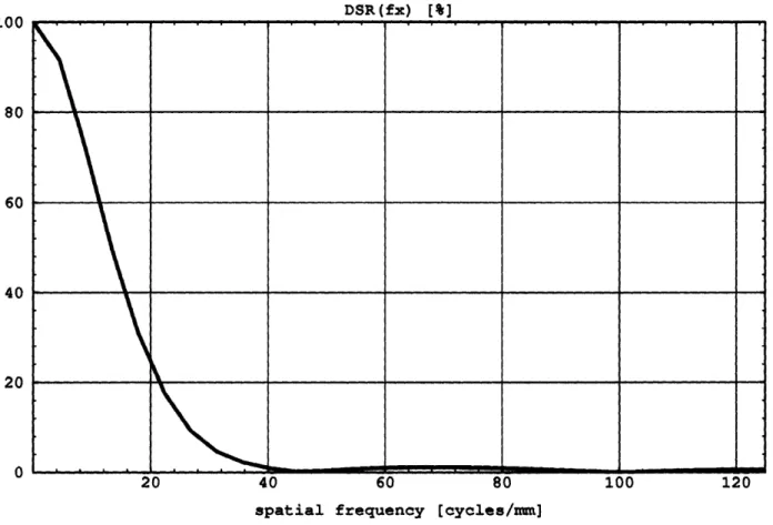
The results presented here are found to agree with this theorem. The direct space data were discrete Fourier transformed in Mathematica on the SPARCstation2. Aliasing is assumed to be negligible for these data taken on 4 Asm steps. Figure 3-6 shows a theoretical diode response to LWIR illumination
I _
____--- ~
I
by an infinitesimally thin slit, traversing the diode in the z direction. Figure 3-7 is its transform, the
diode profile MTF in the z direction. Figures 3-8 and 3-9 are the analogous data for y. Since the a and y directions are symmetric, these curves match the curves for z exactly. Figures 3-10 and 3-11 show the response due to an infinitesimally small LWIR spot in the just the z and the y directions. Figure 3-12 shows the entire response for all z and y. Figure 3-13 shows a profile slice of the full two-dimensional MTF. This matches 3-7, the transform of the slit response, exactly. Figure 3-14 indicates the profile slice for the y direction, matching with Figure 3-9. Finally, Figure 3-15 shows the full Small Staring pixel MTF, the transform of the response given in Figure 3-12.
dsr(x) [%]
x [um]
Figure 3-6: Small Staring Array simulation. The diode slit response(z) is the normalized collected photocurrent versus location of an infinitesimally thin slit of LWIR illumination. Its transform is the a direction profile MTF of the diode.
100. 10. 1 0.1 0.01 0.001
DSR(fx) [%]
100
80
60 40 200
spatial frequency [cycles/mm]
Figure 3-7: Small Staring Array simulation. The Diode Slit Response(f.) is the profile MTF of the diode in the a direction.