Active Filters for 1 MHz Power Circuits
Under Strict Ripple Limitations
by Leif E. LaWhite
Submitted in Partial Fulfillment of the Requirements of the Degrees of Bachelor of Science and Master of Science in Electrical Engineering and Computer Science
at the
Massachusetts Institute of Technology
February 1987
( Massachusetts Institute of Technology 1987
Signature of Author
Department of Electrical/Engineering and Computer Science
January 5, 1987 Certified by Martin F. Schlecht Thesis Supervisor Accepted by Arthur C. Smith Chairman, Departmental Committee on Graduate Students
ARCHIVES
Active Filters for 1 MHz Power Circuits
Under Strict Ripple Limitations
by Leif E. LaWhite
Submitted to the department of
Electrical Engineering and Computer Science on January 5, 1987 in partial fulfillment
of the requirements of the degrees of Bachelor of Science and Master of Science in Electrical Engineering and Computer Science
Abstract:
Recent advances in MOSFET technology have moved the switching frequencies of power circuits into the mega-Hertz range. The drive to these higher switching frequen-cies is motivated entirely by the smaller energy storage elements that supposedly result. Unfortunately, at these very high frequencies, the allowable ripple levels on the input and output of the power circuits are often much lower than they are at lower frequencies.
This then requires greater ripple attenuation which means that all of the desired energy
storage reduction cannot be achieved. As switching frequencies are pushed higher, the passive filtration elements often come to dominate the size and cost of the converter.
In many cases, however, some of the large, costly, passive filter elements can be replaced with small, simple, active circuits. The result is savings in cost, size, and weight, of the overall filter. It is the purpose of this thesis to outline these cases and develope these active circuits.
The thesis first describes the situations in which these active filters find their greatest import. It then moves on to developing the theory and evaluation criteria surrounding these filters. After discussing in depth, the various filter topologies, and available active devices, it presents a working circuit which was constructed in the lab. The performance of this circuit agrees quite closely with both theory and simulation, verifying all of the previous analysis.
Thesis Supervisor: Dr. Martin F. Schlecht
Acknowledgements
I owe thanks to many people for their help in the research and writing of this thesis.
Foremost is my advisor Marty Schlecht, for his interest, unending guidance, and helpful
prodding during the long research and construction stages of this work.
Also Anne Grossetgte receives many thanks for all the hours she put into proofread-ing, checking equations, and commenting on the many rough drafts.
Andy Goldberg, Barry Culpepper, Leo Casey, and Chris Wright have all helped out when in a pinch I needed a few electrical components or bits of inspiration.
Contents
1 Introduction
1.1 Outline ...
1.2 Previous Work in This Area ...
2 Ripple Filters for Power Circuits
2.1 Second-Order Filters. 2.2 Fourth-Order Filters.
3 Active Filters - Overview
3.1 Inductor-Enhanced Current-Filters.
3.1.1 Inductor-Enhanced Filter with Standard Drive .
3.1.2 An Alternate Inductor-Enhancing Drive Topology
3.1.3 Alternate Inductor-Enhancing Sense Circuit .... 3.2 Capacitor-Enhanced Voltage-Filters ...
3.2.1 Capacitor-Enhancing with Standard Drive Method 3.2.2 Alternate Capacitor-Enhancing Drive Circuit . . .
3.3 Effects of External-Source Impedance ...
3.4 Summary ...
4 Practical Circuit Considerations
4.1 Three Terminal Active Device Model ...
4.2 Single Active-Device Filter Circuits ... 4.3 Multiple Active-Device Filter Circuits ...
4.3.1 Separation into Sense and Drive ... 4.3.2 Inductor-Enhancing Filter Circuits ... 4.3.3 Capacitor-Enhancing Filter Circuits ...
5 Applied to Real Devices
5.1 Bipolar Implementations .
5.1.1 5.1.2 5.1.3 5.1.4
Modifications to the Three-Terminal Model .
Values for Model Parameters ...
Limitations of the Model ... Inductor-Enhancing Circuits ... 5.1.5 Capacitor-Enhancing Circuits .. 8 10 10 11 . . .. . . 11 . .. . . 12 14 14 14 19 24 26 26 28 30 33 34 35 36 39 39 40 46 54 54 54 55 56 56 59 . . . .
5.2 FET Implementations.
5.2.1 Modifications to the Three-Terminal Model ...
5.2.2 Values for Model Parameters ...
5.2.3 Inductor-Enhancing Circuits.
5.2.4 Capacitor-Enhancing FET Circuits ...
5.3 Conclusions ...
6 Filter Implementation
6.1 Goals of the Design ...
6.1.1 Power Circuit Specifications . 6.1.2 Noise Specifications.
6.2 Passive Filters to Achieve the Required Filtration ...
6.3 Amplifier Topologies.
6.3.1 Class A, Single-Ended.
6.3.2 Class B, Push-Pull . . . .
6.3.3 Power Dissipation vs. High Gain ... 6.4 Low Frequency Roll-Off of the Loop-Transmission.
6.5 An Input Current-Ripple Active Filter ...
6.5.1 Low-Frequency LT Consideration ...
6.5.2 Gain and High-Frequency LT Calculations ... 6.5.3 The Real Circuit ...
6.6 Summary ...
7 Conclusions
7.1 Future Work
A SPICE Runs
A.1 First SPICE Run ...
A.2 Second SPICE Run ...
A.3 Third SPICE Run ... A.4 Fourth SPICE Run ...
A.5 Full SPICE Run.
62 62 62 63 65 66 68 68 68 69 70 71 71 71 71 72 73 73 75 75 82 84 84 86 86 89 91 94 97 . . . . . . . . . . . . . . . . . . . .
...
...
...
...
...
List of Figures
1.1 MIL-STD-461B CE03 Current Ripple Specification .
1.2 Power Circuit with Fourth-Order Ripple Filter . . . 2.1 Filters for Power Circuits ...
2.2 Fourth Order Passive Filters. ...
3.1 3.2 3.3 3.4 3.5 3.6 3.7 3.8 3.9 3.10 3.11 3.12 3.13 4.1 4.2 4.3 4.4 4.5 4.6 4.7 4.8 4.9 4.10 4.11 4.12 4.13
An Inductor-Enhanced Current-Filter Circuit. Bode-Plot of Gain for Inductor-Enhancing Circuit. Circuits for LT Derivation ...
Bode-plot of Loop Transmission ... Bode-plot of gain/LT ...
Alternate Drive for Inductor-Enhanced Circuit ... Bode plot of gain ...
Bode-Plot of Gain/LT ...
Pole-Zero Plot for gain with Zout = 1/sCb. ... Alternate Sense for Inductor-Enhanced Circuit ... Capacitor-Enhancing Circuit with Standard Drive. LT Circuit ...
Alternate Drive for Capacitor Enhanced Filters ... General Three-Terminal Model ...
Four Simplest Active Filters ...
Block Diagrams of Four Active Filters ... Two Good Sense Connections ... Four Drive Arrangements ... Four Inductor-Enhancing Circuits ...
Bode-Plot of Gain for Four Inductor-Enhancing Circuits ...
Two Different LT Circuits ...
Bode-plot of gain/LT for Four Inductor Enhancing Circuits
Two Good Sense Circuits ...
Four Drive Circuits ...
Eight Capacitor-Enhancing Circuits ...
Bode Plot of Gains for Capacitor-Enhancing Circuits ... 5.1 Model for Bipolar Transistors ...
8 9 11 12
... ..
15
... .. 16
. . . 18... .. 18
. . . 19... .. 20
... .. 21
... .. 22
... .. 23
... .. 24
... .. 26
... .. 27
... .. 28
... .
35
... .
36
... .
38
40 . . . . 41... .
42
... .
43
... .
44
... .
45
... .
46
.. .. 47... .
48
... .
50
555.2 Bipolar Implementation of Inductor-Enhancing Circuits . . . ... 57
5.3 Bode-plot of Gain for Bipolar Inductor-Enhancing Circuits ... 58
5.4 Four Bipolar Capacitor-Enhancing Circuits ... 60
5.5 Model for Field-Effect Transistors ... 62
5.6 JFET Implementation of Inductor-Enhancing Circuits ... 63
5.7 Bode-plot of Gain for JFET Inductor-Enhancing Circuits ... 64
5.8 Bode-plot of Gain/LT for FET Inductor-Enhancing Circuits ... 65
5.9 Four FET Capacitor-Enhancing Circuits . . . ... 66
6.1 Prototype Power Circuit and Fiiters ... .. 68
6.2 Biased Input Current-Ripple Filter ... .. 73
6.3 Small-Signal Loop Transmission Circuit ... 74
6.4 Complete Input Current-Ripple Active Filter ... 76
6.5 Photograph of the Current-Ripple Filter Circuit ... 77
6.6 Sinusoidal Response at 1 MHz. . . . ... 78
Chapter 1
Introduction
The drive to higher switching frequencies in power circuits is motivated entirely by the smaller energy storage elements that result. For the same allowable ripple levels at the
input and output of a power circuit, an increase in the switching frequency of a factor
of ten should reduce the energy storage requirements, and hence the size of the filter
elements, by the same factor. As a result, switching frequencies are now being pushed
into the mega-Hertz range.
dB HA
I I
.2 I I 2
.2 2 20 200
f (x106Hz)
Figure 1.1: MIL-STD-461B CE03 Current Ripple Specification
Unfortunately, because of increasingly strict EMI/RFI limitations imposed by both commercial and military standards in this frequency range, much of the desired energy
storage reduction cannot be achieved. For example, under MIL-STD-461B CE03, a
military current ripple specification shown in Fig. 1.1, the allowable input ripple current decreases at 30 db/decade until 2 MHz where it levels off at 10 pA. Thus, a 2nd order LC filter designed to work at 100 KHz would exceed this specification by only 10 db at 1 MHz. This corresponds to an energy storage reduction in the filter elements of only
80 60 -40 20 -0 .02 -r I
1.8, instead of the factor of 10 that was anticipated.
Furthermore, under this specification the allowable ripple levels are mandated as an
absolute, rather than a relative value. A converter drawing 5 A at 1 MHz would therefore
need an input ripple current attenuation of over 100 db to meet this specification. In order to use reasonably sized filter elements and still achieve these high
attenua-tion levels, fourth-order LC filters are necessary. This more complex filter design makes control of the power circuit very difficult however, especially when one is present at
both the input and output ports of the converter.
Lf2 Le1 .... III yyyII
External
_ System . w -Power CircuitFigure 1.2: Power Circuit with Fourth-Order Ripple Filter
If the 5 A, 1 MHz converter mentioned above was supplied from a 60 V bus through a fourth-order input filter as shown in Fig. 1.2, the outer three filter elements would handle very small ripple energies. They would all have to be sized to handle the full dc energies of the converter, however. In this simple example, the dc-energy to ripple-energy ratio for Cf2 is more than 5 x 10⁶.
Since the ripple energies associated with these outer elements are so small, it should
be feasible to replace them with active circuits that provide the necessary high-frequency
impedance. Because they can be integrated, these active circuits should be smaller, lighter, and cheaper than the passive components they replace. These active filter circuits would be constructed such that they handle only the ripple energies associated with the component they replace. Although they would then dissipate these energies,
the loss would be acceptable in return for the savings in size, weight, and cost that
result.
Though such active filters could always have been built, they are just now becoming feasible because of higher switching frequencies in power circuits. At 100 kHz and
below, the allowed ripple levels are generally quite large, so that any active filters would
dissipate objectionable amounts of power. Now that 1 MHz power circuits are being made and subject to extremely stringent ripple specifications, these active filters could
have tremendous practical import.
_f'__ __ f ' __
1.1 Outline
The purpose of this thesis is to investigate the design and implementation of practical active filter circuits for such applications. The document is divided into 7 chapters.
Chapters 1 and 2 introduce the topic and explain where and why active filters are useful for high-frequency power circuits.
Chapter 3 is an overview of some of the desirable and undesirable parameters
con-cerning the design of suitable active filters. Analysis in Chapter 3 is based entirely on generalized circuit elements and serves to identify some of the useful (and useless) circuit topologies.
Chapter 4 specializes the results of Chapter 3 by using a still-general three-terminal
model as a building block for those circuits of Chapter 3. Chapter 5 further specializes
the analysis by adapting the earlier three-terminal model, first to bipolar transistors, and then to field-effect transistors. The analysis in these two chapters is used to select
'the best' active filter topologies for our purposes.
Chapter 6 investigates some of the other topics associated with actually constructing useful active-filter circuits. It then presents a design that was actually built, and eval-uates its performance in terms of a comparison to theoretical performance, and utility
as a ripple-filter for power circuits.
Chapter 7 is a conclusion which summarizes this piece of research and suggests
directions for future work.
1.2 Previous Work in This Area
The idea of using linear active circuits to aid in eliminating the noise generated by
switching circuits is not new. Indeed, any standard linear voltage regulator can be
thought of as working in this area, as it generally attempts to, with the aid of a large filter capacitor, smooth the output of a diode bridge.
Unlike linear voltage regulators, however, these circuits are designed to be used with high-frequency switching converters. In addition, these circuits will be constructed to see only the ripple-energies associated with a given converter. In this way they
will be valuable for use with very-high-voltage and very-high-current converters while maintaining minimal power dissipation. This, along with the difference in operating
frequencies, will make these circuits very distinct from those typically found in linear
voltage regulators.
In his Master's Thesis [9], George Yundt proposed using active smoothing circuitry on the output of switching amplifiers to simultaneously achieve the high-efficiency of a
switching amplifier, and the low noise of a linear amplifier. His work too, differs from
this work in that his active circuitry was designed to follow varying output voltages,
and his switching frequencies were at least a factor of ten below those I am considering.
J. Walker [10] has considered this subject. His circuits, though, are also designed for frequencies ten times lower than what I'm considering, and he only achieves what
Chapter
2
Ripple Filters for Power Circuits
A power circuit normally has a ripple filter at both its input and output. These filters are of two types: Current-filters prevent large ripple currents, generated within the
power circuit, from reaching the external source or load. Voltage-filters do likewise with large ripple voltages.
2.1 Second-Order Filters
Second-order versions of each type of filter are illustrated in Fig. 2.1.
Current Filter Voltage Filter
Figure 2.1: Filters for Power Circuits Standard circuit analysis yields:
in
saw
Vn_ 1
vJ}
s
8
2L fCf + 1
(2.1)The resonant frequency of the filter is wo = 1/V/fTCf. For good filtration, the switching
frequency of the power circuit is generally well above w. In this situation (2.1) is
simplified and re-arranged to:
Thus, if the allowable ripple levels remain the same, an increase in the switching frequency of the power circuit allows Lf and C to be made proportionately smaller. Because these passive filter elements represent a significant portion of the total size, weight, and cost of the power circuit, reducing their value is of great importance. This
is the motivation behind the drive to high switching frequencies in power circuits. As
discussed in the introduction, however, the allowable ripple level is often more stringent
at higher frequencies. In fact, the necessary filtrations are often so large that these second-order filters are not practical at all. In this situation, higher-order filters are
necessary.
2.2 Fourth-Order Filters
w
Current-Filter Voltage-Filter
Figure 2.2: Fourth Order Passive Filters
Fourth-order versions of the two filter types are shown in Fig. 2.2. These can be
evaluated on the basis of how much 'better' they perform than the second-order filters they replace. In the current-filters, for example, the fourth-order filter can be formed
by starting with the second-order version from Fig. 2.1. C is left unchanged while Lf
is split into two separate inductors L, and Ld such that L, + Ld = Lf. An additional
element, Cb in this case, is then added between the two L's to complete the formation. An exactly dual transformation is carried out to form the fourth-order passive
voltage-filter.
For the fourth-order passive filters above resonance:
to ;Z 1 1= Sw1 84L,LdCbCf Lf Cf2.3 vo- ;to I - = 1 (2.3) vw 8s4CaCdLbLf sCef L1 where Leff !82Le.LdCb (2.4)
Cf -- 8
2C.CdLb
The latter relation in each line of (2.3) looks exactly like the second-order relations
fourth-order over second-order filters could be defined as: gainpay -L. gainpaas -- Cfl
f
s2C CCdL CJRecalling that L, + Ld = Lf and C8+ Cd = Cf, and defining
Lp
LlLd
=L
+
L
and
CpC I
Cd =the gains of the fourth-order filters can be re-written as: Current Filter:
Voltage Filter:
gainpa = 2LCb
gainpass = 2CpLb
These 'gains' were achieved at the 'cost' of an extra element in both filters. The active filters to be described later will also achieve their gain at the cost of additional components. A basis for judgement of the active filters will, therefore, be the relative cost of these extra components.
Also, in situations where the equations are of an appropriate form, the gain of an active filter will be compared to the gain of these fourth-order passive filters. The
emphasis here will be to show that active filters provide many times more gain to
second-order filters than is possible with a simple transformation to a fourth-second-order filter. (2.5)
(2.6) Cs Cd
C. + Cd
Chapter 3
Active Filters - Overview
In the last chapter, 2nd-order filters were modified by splitting one of the elements and adding a new element. The resulting circuit performed better than the original. In this
chapter, active filter circuits will be formed by again starting with a 2nd-order filter,
splitting one element and adding active circuitry. The active circuitry for the current
and voltage filters will be developed separately. There are several different topologies for each type of filter. The first will be developed in detail, subsequent ones will be just
summaries of the resulting equations.
3.1 Inductor-Enhanced Current-Filters
In the active current-filter, Cf is left unchanged while the inductor L! is split in two.
Active circuitry, rather than a passive capacitor, is then added to make these two inductors appear larger. The factor by which the two inductors are made to appear larger will be referred to as the 'gain' of the active filter circuit.
3.1.1 Inductor-Enhanced Filter with Standard Drive
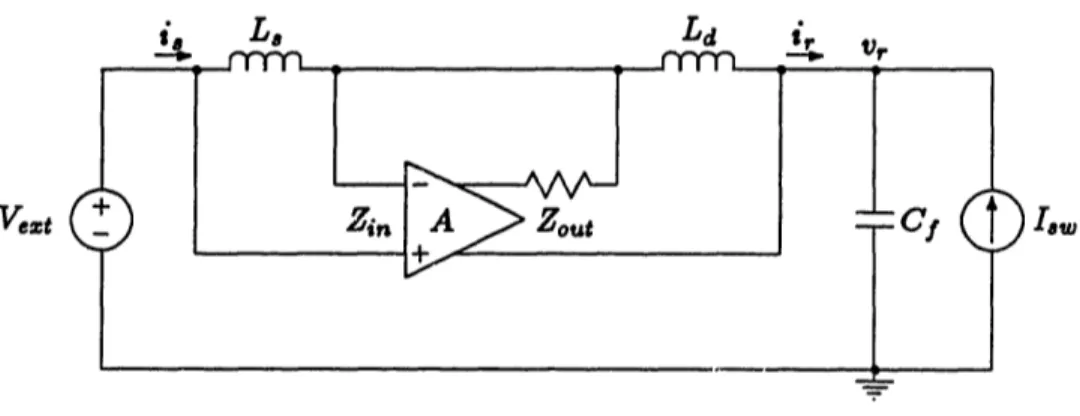
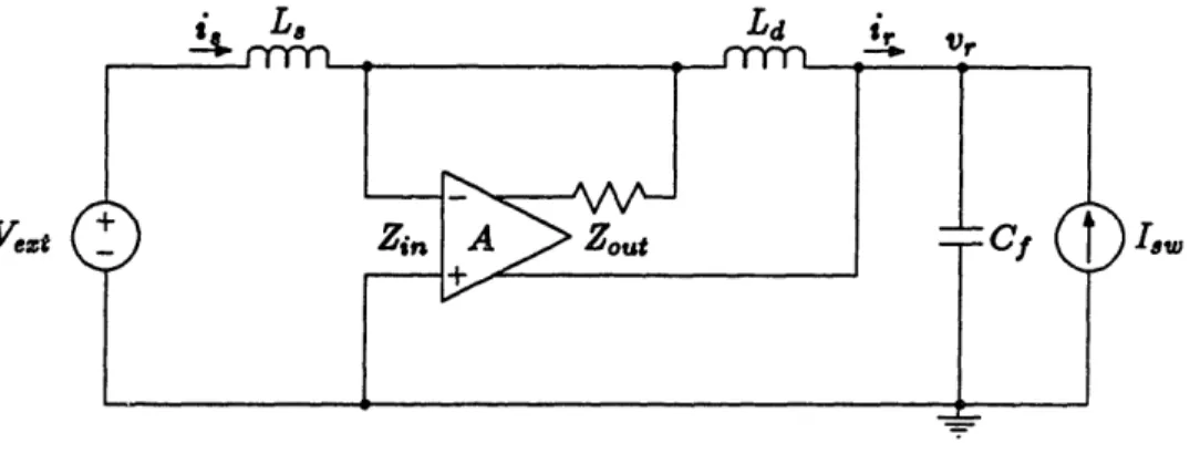
Consider the 2nd-order inductor-enhanced filter shown in Fig. 3.1. The amplifier is characterized by its input-impedance Zi,(s), gain A(s), and output-impedance Zot(s). Though these parameters, and many others to come, are functions of , the (s) will typically be omitted from the equations for compactness.
The external-source ripple-current, i., flowing through L. and Zi, creates a voltage across the amplifier input. This voltage is amplified and placed across Ld with polarity such that i will be driven to zero. If A were infinite, then the filter would be perfect
and i would be equal to zero, as desired. A will not, however, be infinite, so a more quantitative derivation is necessary.
Gain Calculation
To determine the inductor-enhancing gain, the effective impedance Zff is defined as the ratio of the filter-capacitor ripple-voltage, v,, to the external-source ripple-current,
Vcet
Figure 3.1: An Inductor-Enhanced Current-Filter Circuit
is. In this case, since i = i, and the Ve,,t source is an incremental short,
Thevenin-impedance seen to the left of Cf. The exact relation for Zff is:
, _ 8{8L.Ld[(A + 1)Zin + ZoutJ + (L. + Ld)ZinZout}
Zff
=i.
(8L + Zin)(Ld + Zout)Making the substitutions:
Lp L.IILd =
TLL
wd,
-Wd-
and re-arranging yields:
Z,ff is the
(3.1)
8a8Lp[(A + 1)Zin, + Zout] + ZinZout}
Lp(8 + W)(8 + Wd) (3.2)
Lff is defined as Ze/s and is the effective inductance of L,, Ld, and the amplifier.
This Leff could be used in (2.1) to find the attenuation for this filter.
sLp[(A + 1)Zin + Zout] + ZinZout cL
61 = Lp(8 + W,)(8 + Wd)
The inductor enhancement, or gain, of the circuit is then Lff /(L, + Ld). Making this
substitutions gives:
gain = (L+)
(L. L
8Lp[(A + 1)Zin + Zout] + ZinZout
L,Ld(8 + w,)(s + Wd)
For any reasonable amplifier gain A, the '+Zot]' term in the numerator can be
neglected and the relation can be simplified to:
(3.4)
Iw
Zff =
where
Zout (A + 1)LI
For future reference, re-substituting for wz, wJ, and Wd gives:
gain s Zi[(Lp(A + 1) + Z,] (3.6)
(L + Zin)(Ld
+ Zout)(3.6)
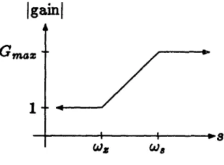
gain 1-L---~- i -- 8 WS WA s,Wd Wd C,WFigure 3.2: Bode-Plot of Gain for Inductor-Enhancing Circuit
A Bode-plot of this expression, assuming that A, Zi,, and Zo,ut are real, is shown
in Fig. 3.2. The value of G,,a depends on the relative values of ws and Wd. The two possibilities are:
o,
< Wd
G,.
= (A+ 1)
W+ .WLL,
d
iL
= (A+ 1)3.
+ Wd(3.7) W > Wd Gm, az = (A +1) L
Notice that these two look identical except for the factor of Ws/Cd in the first. /Wd
in this region is < 1, though, so the highest gain is achieved by using wo > Wd. In this
realm, this circuit makes L, and Ld appear larger by a factor on the order of A. Maximum Effective Inductance
Another important feature to notice is that, for a given working frequency owf, there is a fundamental limit on the maximum effective inductance, Lcffms., that can be created with this circuit. Qualitatively, this can be understood by working backwards from the standard gain derivation. From (3.4), Lff = gain x (Ls + Ld) which indicates that L,ff is linear in (L. + Ld). Unfortunately, increasing L, and Ld arbitrarily does not result in correspondingly large values for Lfe because the gain is a function of L, and Ld.
As L. and Ld are raised in an attempt to raise Lff, Ws and wd of the gain relation
are correspondingly lowered. As the higher of ws or wd crosses below the working
stop increasing with L and Ld, and instead will hold constant at a value given by the
gain relation (3.6) above both w, and wd.
From (3.28), when wf is greater than w, and wd:
Leffm.6, = (A+ 1) (3.8)
which is no longer a function of L. or Ld.
Thus, though this circuit provides inductor-enhancement, or gain, for values of L, and Ld which cause the operating frequency to be between the two poles, there is a maximum value for the effective-inductance it can produce even when L. and Ld
are made very large. This may prove to be a serious problem if the applicable
ripple-specification and power circuit demand an inductance in the current-filter which is above
Leffm.s-The Loop-Transmission
The active filter circuit is a feedback structure, and as such has an associated loop trans-mission (LT). The characteristics of the LT govern the stability of the filter circuit. Generally, the loop transmission will be closely related to the gain, and will have mag-nitude much greater than 1 at the circuit's working frequency. The frequency at which
the ILTI = 1 is commonly known as the 'unity-gain-crossover' (UGC). Bear in mind
though, that the 'gain' in the UGC is really a misnomer, for in these circuits the gain and the LT are quite distinct.
Above the working frequency, the LT will have to be 'rolled-off' so as to make the UGC occur before the angle of the loop-transmission, (LT), is equal to 1800. The most
sure-fire way to accomplish this is to roll-off the LT with a single 'dominant' pole and
force all other poles to be above the UGC.
Gain/LT Figure-of-Merit Since the LT roll-off is being accomplished with a single
dominant pole, there is a definite relationship between the UGC and the maximum
possible value for the LT at the working frequency (LTU,,,):
LTw. , UG (3.9)
All the parasitic poles of the circuits must be above the UGC, however, so raising
the UGC will be difficult in practical implementations. To achieve a given gain,
there-fore, the circuit which has the lowest UGC will undoubtedly be the easiest circuit to
successfully implement. Since LTwf,,. cc UGC, the circuit with the lowest LT1wf will also be the one with the lowest UGC. The objective then is to construct active filter circuits with the highest possib!e gain/LTf ratio. The gain/LT will, therefore, become
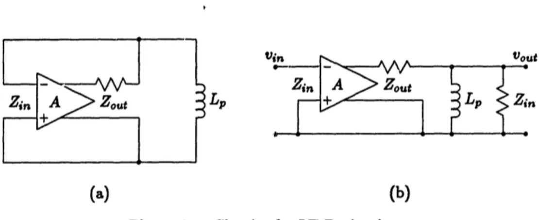
Zin A Zout
+S
(a) in - ~ A AA AA Vout _- V --ZrnA Zout+
>
ffI
(b) Figure 3.3: Circuits for LT DerivationLT Derivation The LT is found by incrementally shorting both C and Vet. The resulting circuit, shown in Fig. 3.3a, is then 'broken' and 'loaded' to become that of Fig. 3.3b. The vout/vi, relation is then the LT for the original circuit.
A short derivation yields:
LT Vot = A
Vin
where
Zin Zout
in + Zout A bode plot of this simple relation,
shown in Fig. 3.4.
(
Zn
Zn + Zout sLp sL+ P
(3.10)and
wp-L
again assuming real amplifier parameters, is
again assuming real amplifier parameters, is
ILTI A Zi.+Z,,tz
-wp
s
Figure 3.4: Bode-plot of Loop Transmission
Notice that this LT rises with a slope of 1 until wp where it levels off at a value of
AZi,/(Zout + Z,,t). To accomplish the LT roll-off discussed above, a pole will have to
be added to the LT by modifying A(s). This pole can theoretically be placed anywhere that adequately rolls-off the LT to keep the UGC below the parasitic poles of A(s). Bear 1See [4], Chapters 1-4, for a complete discussion of the LT, its identification, and its implications on
the stability of feedback circuits.
-., m 4 F - w w - --- I LP
in mind, however, that a pole in A(s) to roll-off the LT, will also appear as a pole in the gain expression, eq. (3.5). To maintain maximum gain, therefore, it will generally be
desirable to place this additional pole at, or just above, the circuit's working frequency.
Gain/LT Calculation
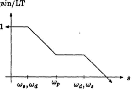
The figure-of-merit is the gain/LT ratio. Well above the zero in (3.6):
gain ( sL + Zp )
(3.11)
-
Ps(Zi. + zw)
(3.11)
LT (sL. + Zi.)(sL + Zout)
It is easy to show that the zero in this expression is always between the two poles. A bode-plot, therefore, looks like the one shown in Fig. 3.5.
g~Jn/LT
14-I. D
Wa) Wd _P WdjWe
Figure 3.5: Bode-plot of gain/LT
From this simple analysis, it appears that the best performance will be obtained by operating below all the poles and zeroes of the gain/LT expression. This corresponds to the slope=+1 section of Fig. 3.2, so for maximum gain, 0w and wd should be placed ju'st above the operating frequency.
Even so, the gain/LT ratio for this circuit has a maximum value of 1. Thus, from (3.9), this circuit has a maximum gain:
gain,, = LTufm = UG (3.12)
WJ!
as dictated by the maximum value for the UGC which is still below all the parasitic
poles of A(s). For circuits intended to work at 1 MHz and above, this becomes a definite limitation on the gain; pushing the UGC, and hence all the parasitic poles significantly above 50 MHz can be quite difficult.
inductor-enhanced circuit in Fig. 3.1 by sliding the negative output lead of the amplifier through the filter capacitor, Cf, to ground.
Vezt 18w
Figure 3.6: Alternate Drive for Inductor-Enhanced Circuit
A qualitative explanation of the difference between this and the previous circuit follows. The previous inductor-enhanced circuit can be thought of as imposing a non-zero voltage across Ld so as to cancel v, and leave the 'middle node' at incremental ground. This circuit, on the other hand, can be thought of as trying to directly hold the 'middle node' at incremental ground. While the amplifier output voltage used to
be approximately v, plus the voltage on Zout, it is now only the voltage on Zo,t. The
current through, and hence voltage across, Zot is roughly the same in both. The output voltage of the amplifier is also related to i, by the same equation in both. Thus, for the same v, this latter approach ought to yield a smaller i. This translates into larger
Lff and therefore a larger gain.
Gain Calculation
For a quantitative derivation, the first thing to realize is that i, does not equal i, anymore. Thus Zff-v,./i, is no longer the Thevenin-impedance as seen from Cf. Instead,
Zef = + )Zou + (A+)Z A(L+ [ P Zout + (A 1)Zin (3.13)
Z,.t (.L. + Zi,)
which has a single pole and a single zero. The gain is again Zeff/s(L + Ld):
gain
= Zout
+
(A
+
)Z,
Zout
+
(A
+ 1)Zin .
r a r a gain( ,
Z,)
(3.14)
to the '(A + 1)Zi,' terms. Making this simplification yields:
gain = (Zin sLp(A + 1) + Z,,t (3.15)
Zout sL, + Zi.
Notice that this relation looks much like (3.6), the only difference being the absence
of 'Ld+' in the denominator here. A bode plot of this expression is shown in Fig. 3.7.
Igainl
1-I, I I - 8
i.~ -i.J
WX w8
Figure 3.7: Bode plot of gain Above both the pole and the zero the gain is maximized at
Ld / Zin \
gain,, =
(A
+1)L
+ L
(3.16)
which looks exactly like the wJ < wd relation in (3.7). Thus at a first glance it appears as though this circuit is no better than the circuit from Fig. 3.1. Closer investigation, however, shows that the gain of this circuit can be made quite large by making Zout small. On the other hand, making Zout small in the previous circuit lowers wd until the
assumption that w, < wd is violated. Once this happens, the gain of the previous circuit
stays at the w, > wd value while the gain of this circuit keeps increasing as Zut is made smaller.
Maximum Effective Inductance
This circuit has the added benefit of having no fundamental limit on the maximum effective inductance it can create. This fact can easily been seen by starting with
the working frequency, wuf, in the high gain region defined above, and substituting
L,ei = gain x (L, + Ld) into (3.16):
Lff = (A+ 1)Z Ld
(3.17)
LT Analysis
The LT is again found by incrementally shorting both C and Vet. This results in the
same LT circuit as in Fig. 3.3, so the LT is the same as in (3.10).
Gain/LT Calculation
The general figure-of-merit is again the gain/LT ratio:
gain
Zin
+
Zout
(sLy
+
(+Zp)
(sLpy
LT
Zt
((+
LT ZOut J (sLp) (9L, + Zi.) (3.18)
This expression has a pole at the origin, two zeroes, and another pole. Substituting the
old definitions for w,, w,, and wp yields:
gain
Zi
+
Zt
(
Ld
(8+
W)(8 +p)
LT oUt LJ L.+Ld S(s+ w.)
A Bode-plot of this expression looks like Fig. 3.8.
(3.19)
gain/LT
oW > Wp,
8 Wz
Figure 3.8: Bode-Plot of Gain/LT
From this Bode-plot, we see very quickly that if w, > wp this topology can indeed yield gain/LT > 1 by operating above all the poles and zeroes. In the previous topology, the gain/LT was always < 1. Maximum gain/LT is achieved by making:
W,
p
Zi + Zout
Zot
(
Ld )> 1
(3.20)The region below w, also looks tempting for gain/LT> 1, but closer inspection of
(3.15) reveals that the gain=1 in this region, so it is not of particular value.
Using a small L. and a large Zi, to raise w, almost to the operating frequency, and
a large Ld and small Zout to lower wp yields:
gain Zi.
T Zout (3.21)
c O~
which might be 10 to 100. Also under these conditions:
gain = (A+)
n L
Ld
A -A (3.22)Zout=(a~l)$( L. + Ld
·
Zoutwhich can easily be in the 1000 range. Thus, this circuit allows for quite high gains with reasonable UGC's, and it therefore seems to be superior to the earlier circuit. The requirements of a particular application, however, may alter that conclusion. For
example, if the DC bus voltage of the power circuit is to be very high, it might be much
easier to let the active-filter circuit 'hang from the bus', as in Fig. 3.1, than it is to place the amplifier output across the bus, as in the circuit of Fig. 3.6.
Consideration of Zout
At present, the output of the amplifier in this circuit is connected through Zout directly
across the (potentially very high voltage) DC bus. In most cases, this mandates that
Zout contain at least a DC blocking capacitor. This capacitor sees the full DC bus
voltage and is hence considered 'expensive' and should be made as small as possible. The above equations, however, call for a low Z,.t at the working frequency to achieve
high gains. This factor will undoubtedly determine how small the DC blocking capacitor
can be. Assuming that Z,,t looks predominantly capacitive, (Zut = l/sCb) as would
be the case for a 'small' DC blocking capacitor, the gain can be derived to be:
gain = 82LpCb(A +
1)Z. +
sL+Z (3.23)(sL. + Z,.)
Because A in the s2 term is quite large, the zeroes are a 'lightly damped' complex pair.
A typical pole-zero plot is shown in Fig. 3.9.
iw o0
Wa
0
-a0'
Figure 3.9: Pole-Zero Plot for gain with Z,,ot = 1/SCb.
Here there is no maximum gain; even above the pole the gain continues increasing
with slope=1. Above the complex zero pair, but, below the pole at w,, the gain can be simplified to:
Bear in mind that this relation is only valid where Z,,ot looks predominantly capacitive. At and above some frequency, the 'real' output impedance of any practical amplifier will
come to again dominate Zot. Whether this analysis, assuming capacitive Z,,ot, or the
previous analysis, assuming real Zout, is valid is determined by the operating frequency relative to this 'drive pole.'
Comparison to Fourth-Order Passive Filters: If Zot does indeed look capacitive at the operating frequency, then it is beneficial to make the following observation. The gain of this improved circuit was achieved at the cost of the active circuitry plus that of Cb. Similarly the gain of a fourth order passive filter, (2.7), was obtained at the cost of just Cb. Thus, the gain of this active filter compared to the gain of the fourth-order passive filter gives a measure of the relative worth of the active circuitry. Dividing (3.24)
by (2.7) gives:
gain,,t
Ygain
8 5 A + 1 (3.25)
Thus, for the same Cb, this active filter circuit has A + 1 times more gain than the
fourth-order passive filter.
3.1.3 Alternate Inductor-Enhancing Sense Circuit
There is a similar transformation for the sense leads of the amplifier. Shown in Fig. 3.10,
this new topology is obtained by sliding the left input lead of the amplifier in Fig. 3.1 through the incrementally shorted V,,t.
Vezt 1.0
Figure 3.10: Alternate Sense for Inductor-Enhanced Circuit
This simple transformation results in a couple of important differences to the circuit's operation. First, note that the amplifier input-current no longer flows through Vezt. Under most circumstances, this should be beneficial for it should serve to reduce i.
The most important difference, though, is what might happen if Vezt were not an incremental short. Ordinarily, this would be considered good, for the ripple current
drop across that non-short would add to the drop across L, and yield a larger sense
voltage. If, however, V,,t looked capacitive, there exists a series LC circuit on the
left-hand side of the filter. If that C happens to resonate with L. anywhere near the
switching frequency, i could be huge with no detectable voltage at the input-terminals of the amplifier. For this reason, this alternate sense topology is considered too prone to failure to use.
3.2 Capacitor-Enhanced Voltage-Filters
let
VulFigure 3.11: Capacitor-Enhancing Circuit with Standard Drive
As could be expected, the analysis of the capacitor-enhanced voltage-filter circuits is very much the dual of the analysis for the inductor-enhanced circuits. Capacitor-enhanced circuits are constructed from the 2nd order voltage-filter of Fig. 2.1. L! is left unchanged, while Cf is split into C, and Cd. Active circuitry is then added to make C, and Cd appear larger.
3.2.1 Capacitor-Enhancing with Standard Drive Method
One possible arrangement is shown in Fig. 3.11. (Note that the amplifier is a
current-in/current-out amp). The amplifier input-current, ii is due to the ripple-voltage at the external-source, ,. This current is amplified by a factor of A and drawn from the external-source terminals so as to drive v, to zero. Again, if A were infinite, v, would
equal zero, as desired.
Gain Derivation
The effective-admittance, Yff, is defined as the inductor ripple current i over the external-source ripple voltage v,. Since v, = v, in this case, it is also the Norton-admittance. The exact solution for Y6ff is:
i, (sC, + Yin)8CdYout + sC.YinYot + (A +
1)
SCCdYin (3.26)Y,.
, = , (sC,. + Y,)(ScCd + Yo.,) which is ezactly the dual of (3.1).Defining
CP -
W
6C -Yin./C(Y-,,el ' ! (3.27)
gain 8(C + Cd)
t-You/Cd
and performing an analysis very dual to that in the inductor-enhancing discussion yields:
[Yi[Cp(A + 1) + Yout] = (A+1( Yin. + 8 W (3.28)
(8ga + Y
)
(8C, + Y(t)
+ C
(+ w,)(s + Wd)The bode plot of this expression looks exactly like Fig 3.2. The two possible values for Gma2 are:
ws < Wd gain (A + 1), + C(329
C.W +>CdWdTt (3.29)
J > d gain (A+
1)
+CaAgain, the maximum gain is obtained by working in the w, > wd region.
An important special case of this equation is the result obtained by assuming that the current source in the amplifier is 'good'. Under this assumption Yot z 0 and the
gain relation, (3.28), further simplifies to:
gain (C CA) C + 1)Yi, (3.30)
C,+(
Cd )(AC+ Yi,
Maximum Effective CapacitanceAn argument exactly the dual of that used in section 3.1.1 holds here regarding the maximum effective capacitance that this circuit can create at a given working frequency. The maximum effective capacitance is found by substituting Cff = gain x (C. + Cd) into the gain relation and evaluating above both poles:
Cff,,, = (A+
1)
,
(3.31)
LT Analysis
The LT of this circuit is found by incrementally opening both the input and output
ports. The LT circuit looks like Fig. 3.12.
out
After a bit of derivation, the exact dual to (3.10) appears:
LT = AYin + Yout scp
+ Yp
(3.32) where YinYoutYp-Yin
+t yut
Gain/LT Calculation
Since the gain and the LT relations exactly dual those from the inductor-enhancing
analysis, the gain/LT does so, as well. These equations, therefore, are presented only as a quick reference. Again, assuming that we are well above the zero in the gain expression,
gain LT
(8CP + Yp) (Yin + Yout)
(8Ca + Yn)(BCd + Yout) (3.33)
The Bode-plot of this looks exactly like Fig. 3.5. As before, the best performance is obtained by placing all the poles and zeroes of the gain/LT expression slightly above the working frequency, and again the gain/LT has a maximum value of 1.
3.2.2 Alternate Capacitor-Enhancing Drive Circuit
Also by duality, there exists an alternate drive topology for the capacitor-enhancing circuits which overcomes the above gain/LT limitation. It is shown in Fig. 3.13.
V51
Figure 3.13: Alternate Drive for Capacitor Enhanced Filters
alter-nate drive. They are:
¥Yc~..t = (C. fCd)
(A +
+ )Yog ++
Yn + YotI,- Yout (8Co + Yin)
gan
eff
VY Li aCp(A + 1) + Youtgainmax = (A + 1) Y3.34)
LT ( A .j 1)C+,
AYin
+
ot
o)
+
gi
T= (Yi.+
~A
W
Y
(c )
,t,
+
(8
+ )(i
8
9(8
+
W.)
+
)
The Bode-plot for the gain/LT looks exactly like Fig 3.8. Again, it appears that this topology is superior to the standard topology because its gain/LT can easily be greater
than 1.
Consideration of Yo,t
If the exact dual of the alternate-drive inductor-enhancing circuit is used, as shown in
Fig. 3.13, Yout will have to carry the full DC bus current. To avoid excessive power
dissipation, therefore, You, must be made to be at least partly inductive. Again, this inductor is considered expensive and should be made as small as possible. If this inductor
is sufficiently small, then Y.ot will look inductive at the working frequency and this will
affect the gain derivation. Assuming, then, that Yot, = 1/sLb the gain relation in (3.34)
becomes:
gain= 2 LCp(A + )Y + Cp + Yin (3.35)
C, -+ Yin
In this situation, the gain has no theoretical maximum and the DC power dissipation in
You is zero. Because A is large, the zeroes are again 'lightly damped' as in section 3.1.1.
Comparison to Fourth-Order Passive Filters Above the zeroes, but below the pole in the gain, a clean active to passive gain comparison can be made. The gain in this region simplifies to:
gain = 2LbCp(A+ 1) (3.36)
so that, just as with the inductor-enhanced alternate drive
ga.nact (A + 1) (3.37)
gain,,+
Thus, for the same inductor Lb, this circuit provides A times more gain than does the fourth-order passive circuit.
LT with Inductive Y,,t It is also valuable to consider the LT when Yout looks in-ductive. Substituting Y,,t = l/sLb, the LT expression becomes:
LT = AY, 82LbCp(3.38) LT = (sLbYin + 1)(8C + Y(3.38)
above the zeroes in the gain, the numerators in the gain and the LT are identical. The
gair/LT ratio above the gain zeroes is therefore:
gain (sLbYin + 1)(8C + Y) (339)
LT A 8C, + Yin
Notice that this ratio increases with a slope of 1 above all of the poles and zeroes. Thus,
this circuit can achieve high gain/LT when operated well above all the poles of the LT.
In this region, the gain is still increasing with a slope of 1 and the LT is level. An
additional compensation pole in A, just below the operating frequency, will serve to level off the gain to a constant value (if that is desired) and start the LT roll-off.
3.3 Effects of External-Source Impedance
In the calculation of the LT for all these circuits, the 'external-source' was always assumed to be either an incremental short for inductor-enhancing, or an incremental open for capacitor-enhancing circuits. Unfortunately, in arbitrary installations this
may not be a perfect assumption so there is some concern as to the effects of these
imperfections.
If these imperfections are small, they should not substantially affect the gain of any circuit, but they may be responsible for introducing a high frequency pole to the LT. If not accounted for, this extra pole in the LT could cause the circuit to be unstable.
Effects on the Loop Transmission
Recall that for both inductor and capacitor enhancing circuits, the standard drive and alternate drive topologies had the Camne loop transmission. Modifying the incremental impedance of the external-source will not change the fact that the loop transmissions for the different drive topologies are the same.
Assuming that V.zt of the current-filter looks like an inductor Lz, instead of being
an incremental short as before, the loop-transmission of the inductor-enhanced circuit
is:
AZisL,Ld
82L.LdL, + 8[Zou.L,(Ld + L,) + ZinLd(L, + L)J] + (L. + L + Ld)ZotZi, (3.40)
Similarly, assuming that I.t of the voltage-filter looks like a capacitor Cz instead of
being incrementally open gives:
AYn8sC Cd
LT = 2
CCdC3 + 8[Yo.tc.(Cd + C.) + YinCd(C, + Cz)] + (C. + C, + Cd)Yout,.n
for the loop-transmission of the capacitor enhanced circuit.
There are several points to notice here:
1. These two are exact duals of each other, as would be expected. 2. They each agree with (3.10),(3.32) in the limit L,C, -. 0.
3. The extra element has introduced an additional pole to each LT relation.
It is this last property which is potentially very harmful. Recall that A(s) contains an appropriate LT roll-off pole. Thus, if this new pole occurs below the UGC, the circuit
will become unstable.
To investigate this new pole further, first assume that the extra element is a circuit parasitic. As such it will be much less than other comparable circuit elements. In this
case, the two LT poles lie on the negative real axis:
L, L,,Ld WP = v °p2 =
Zi+Zg
L
2'L.Ld
l&(3.42)p1r; Wp2Y YI. +Y
C2 << C,,Cd Wp = Wp2 = CZ
In both relations wpo is the old LT pole at wp, and the Wp2 is the pole introduced
by the new element. Notice that Wp2 is a factor like Lp/Lz or Cp/Cz higher than wpl. Since ILTI is generally quite large at wp it is still possible that Wp2 will occur below the
UGC and hence cause the circuit to be unstable.
The only solution to this problem seems to be to add extra Lz or Cz to the circuit and try to move wp2 down to be the dominant LT roll-off pole. This further requires
removing the old LT roll-off pole from A(s), or at least moving it to above the UGC. In practice, this would require a fairly large Lz or Cz. As such, it would be
sig-nificantly larger than other comparable circuit elements. With this in mind (3.40) and
(3.41) simplify to:
L, »> L,, Ld LT = AZsLLd
L, > 2L,Ld + s(L.Z,ut + LdZi,) + ZoutZin]
(3.43)
C
2 >C.,Cd
C >>
C
C,,
LT
LT = C,[s
= 2CCd + s(C.Yout
AYs
8+ CdYi.) + YotY,,]
Cd
The denominators of these can be easily factored to yield:
Lz
>
L,, Ld LT = s_
______
o
( + wd(3.44)
sAY;
Cz > C,,Cd
LT = C
sAYi
Thus, making Lz or C. large has moved the two poles of the LT, wpl and Wp2, to
Effects on Gain
New values for the effective-inductance, L f/, and effective-capacitance C* f/ are:
L/ = L + L.ff = L2+ gain(L. + Ld)
(3.45)
C, = C. + Ce! = C. + gain(C, + Cd)
Thus, until Lz or C. get to be on the order of Lff or Cff (hopefully very large), their addition will not appreciably effect L or C*f. On the other hand, ! L. and C. are
'costly' elements, so the gain should be rdefined:
gain' ff A e,
LC + Cd + CL LC
Re-deriving the four gain relations gives and assuming operation above w. gives:
Standard Drive Alternate Drive
gain' .
.a)
n(s-
w)(,
Z +ZoutL,(
+
w)
(3.46)
gain* Ai AAC
c,(8 + W,)(8 + Wd C, +W
Effects on Gain/LT Ratio
Dividing (3.46) by (3.44) gives the general figures-of-merit.
Standard Drive - = 1
gi (a+w)(3.47)
Alternate Drive T (s + Wd)
The latter relation is flat at unity out to wd where it starts increasing with a slope of 1. Thus, even when adding large amounts of Lz or C., the alternate drive topology can
provide gain/LT in excess of 1 for operating frequencies above w, and wd.
Conclusions
In those situations where the impedance of the external-source is unknown, or where it is known to be undesirably capacitive or inductive, the active filter circuits may have to be modified to keep them stable. Though this modification generally has detrimental effects on the gain, it does not make the filters useless. In fact, the alternate drive circuits can still achieve gain/LT ratios significantly greater than unity.
3.4 Summary
Before moving on, it is valuable to restate some of the key points in the development
thus far.
1. There are two different drive topologies for both inductor-enhancing and capacitor-enhancing filter circuits for a total of four active filters under consideration. 2. Both topologies have the potential to provide reasonably high gain.
3. The alternate drive topology can achieve gain/LT > 1 in both inductor and capacitor-enhancing circuits.
4. There is no fundamental limit on Leflma or Cq6 fm=. using the alternate drive
topology.
5. External-Source impedance could make the filters unstable unless specifically
Chapter 4
Practical Circuit Considerations
Thus far, the development of inductor-enhanced and capacitor-enhanced active filter circuits has been centered around generic amplifier modules characterized by their in-put/output relations. Voltage-in/voltage-out amplifiers were used for the inductor-enhanced filters while current-in/current-out amplifiers were used for the capacitor-enhanced filters. The development achieved large gains in both a 'standard' and an 'alternate' drive topology for each filter type. The only task remaining is to develope'optimal' implementations of these amplifier modules.
To be considered a worthwhile endeavor, these active filter circuits ought to exhibit gains in excess of 100 at their 1 MHz nominal operating frequency. Since the gain of these circuits is generally close to the amplifier gain A, gain-bandwidths in the 100 MHz region are required. Also, though the amplifier in these circuits operates at a gain of A, the outer feedback loop in all the circuits imposes unity-gain-feedback stability constraints on the amplifier.
This gain-bandwidth specification far exceeds what is available with generic
op-amps. Special high-speed high-gain op-amps may be able to provide the desired gain-bandwidth, but they cannot be compensated for unity-gain-feedback. Thus commer-cially available op-amps are not suitable for this application.
Instead, special purpose amplifiers will have to be constructed from discrete elements such as bipolar transistors and FET's.
4.1 Three Terminal Active Device Model
A characteristic of the available discrete elements is that they all have three terminals.
As such, relations developed on the basis of a general three-terminal device model can
be easily adapted to the characteristics of a particular device by choosing appropriate
values for the model parameters.
Figure 4.1: General Three-Terminal Model
A simple but adequate three-terminal model is shown in Fig. 4.1. It is a simplified
version of the well known hybrid-7r model. Because this model does not completely
represent the terminal characteristics of the real devices, it will be used only for making
rough comparisons between different amplifier and active filter topologies. MVV
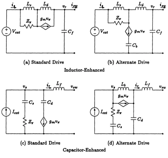
4.2 Single Active-Device Filter Circuits
Active filters can be made using a single active device as the amplifier. Though their
gain is limited by their utter simplicity, they can still be of use in some applications.
There are six ways to connect an active device as the amplifier in each of the four filter circuits under consideration. Fortunately, one connection in each provides higher gain
than all the others and is therefore clearly superior. The 'good connection' for each of
the four active filters is shown incrementally in Fig. 4.2.
(a) Standard Drive (b) Alternate Drive Inductor-Enhanced
w w
(c) Standard Drive (d) Alternate Drive
Capacitor-Enhanced
The gain for each is: gain = gainma =
(a)
8Lp(gZ,
8L
+
+ 1) +
z.L
Ld (gmz + 1)
+
Ld
+
(b) 8Lp(gmZ + 1) + Z L (gmZ + 1) (4.1)(b)
+ ,
1,
Ld (4.1),()
C8
T
+
1)
2C .mZr + s C 4d + 8'Cp£b(g"Z'r8.(d)
+ + 1)+
1
8CpZ ! + Cd (g,,Z1)sL
C+
L+CdThere are several things to notice here:
1. The relations for inductor-enhanced and capacitor-enhanced circuits are no longer duals of each other. This is due to the non-duality of the active device used to create both types.
2. The gain expressions for the capacitor-enhanced circuits look very much like those
from Chapter 3 with Yot = 0.
3. The gain expressions for the inductor-enhanced circuits can be made to look like those of Chapter 3 by letting Zout -,oo, A - oo, and ZutlA - G.
4. The equations for the two inductor-enhanced circuits are the same.
5. The gain,, column assumes that g and Z, look resistive.
6. The gain,,z column is applicable only in certain regions of operation for each
circuit.
For bipolar transistors, for example, gmZ,,-'J 100. Thus, active filters with gains in the 100 region should be achievable with a single bipolar transistor and associated support components. High-frequency compensation of these simple filters should also be very easy for the number of parasitic poles is kept to an absolute minimum. In practice, the required support and bias circuitry would tend to reduce the gain by a
small amount, but for many applications these filters may be quite valuable due to their utter simplicity. In other applications, even more gain is desirable so the analysis
i L. Ld
Vezt
-
-
Sense
-
Drive
7-/
(a) Standard Drive Vezt (b) Alternate Drive (c) Standard Drive (d) Alternate DriveFigure 4.3: Block Diagrams of Four Active Filters
V,
7n7al
J
t
Inductor Enhanced Capacitor Enhanced m< b | I, c .4.3 Multiple Active-Device Filter Circuits
In general, an increase in the number of active devices would lead to an increase in the maximum achievable gain. Unfortunately, each additional active device will also add a
parasitic pole or two to the LT. All these parasitic poles must still be kept above the
UGC. As a result the limit on the maximum achievable gain very soon comes not from how many active devices are used, but from how many poles can be pushed significantly above a usefully high UGC. It is felt that two active devices provides the best tradeoff between number of poles and high gain. Henceforth the development of the active filters
will concern itself with two-device circuits.
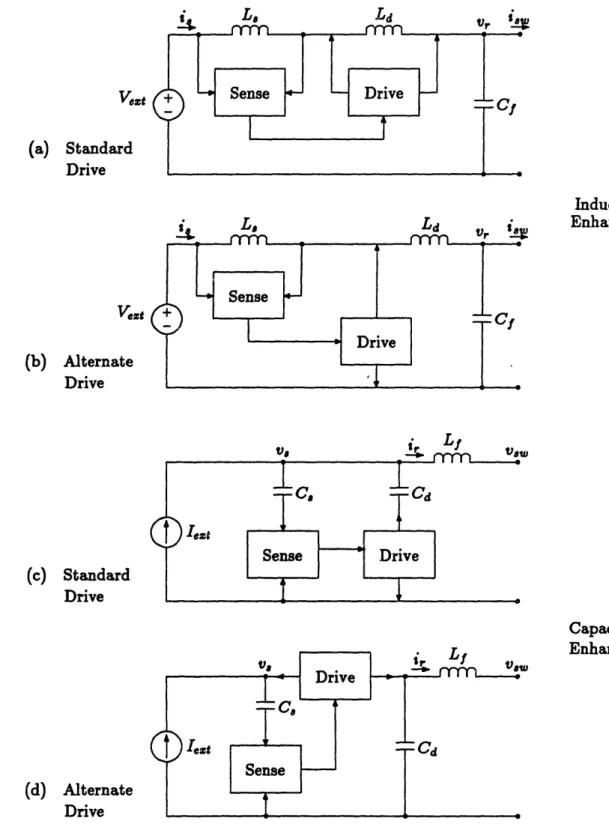
4.3.1 Separation into Sense and Drive
To facilitate further development, each filter circuit will be divided into two sections;
'sense' and 'drive'. Block diagrams of the four active filters developed in Chapter 3
separated into their sense and drive sections are shown in Fig. 4.3. Since each filter will be composed of two active devices, each section will contain a single active device and
4.3.2 Inductor-Enhancing Filter Circuits
Sense CircuitsVezt Vest
(a) (b)
Figure 4.4: Two Good Sense Connections
There are a total of six ways to connect the three terminal element across a
sense-inductor. Frtunately, only the two shown in Fig. 4.4 are of any value. The output of
each of these is a current. Quantitatively:
(a)
=
-gmZr
+
(4.2) (b) = g { L. T
Notice that the signs of these two transfer relations differ. This will become very important when selecting appropriate drive circuits.
A closer examination of (4.4) shows that while in (a), i/i, becomes as high as
gmZ,, in (b), io/i, is always < 1. Thus it seems that (a) is immediately superior to (b). Approach (b) should not be discarded yet though, for in both of these io does not depend upon the load impedance that the sense circuit sees. If working into a high load impedance, (b) might actually 'perform better' than (a) due to miller characteristics. Also the LT characteristics, or sign of i,/i,, of (b) might make it very desirable.
Drive Circuits
As before there are six different connections for an active device in each of the standard and alternate drive topologies. Again, only two in each of the drive topologies are of any value. The four viable drive circuits are shown in Fig. 4.5.
It would be hard to define a meaningful transfer relation with which to compare these various drives as pictured. For an intuitive feel, however, if C to the right of the drive is considered an incremental-short and the sense circuitry to the left an incremental
open, then the inductor-current, iL,, can be derived:
- (gmZr + 1)
(4.3) (c),(f) ti = -gmZr
The most important thing to notice is that, these relations differ.
(c)
just as with the sense circuits, the signs of
TU'
Standard Drive (d) Ld iLd JamT'L=_* ? - fV. j, Zr gmVfr ~1 -' _1 Alternate DriveFigure 4.5: Four Drive Arrangements
(e) (f)
I _ _ b - - * @
1<
-! ·
Total Inductor-Enhancing Filter Circuits
Great care must be taken to observe the signs of the transfer relations when connecting
various sense and drive circuits. To result in a stable circuit, (have negative feedback)
the product of the signs of the sense and drive should be positive. Thus, though there are four viable drive circuits and two viable sense circuits, there are only four viable connections of the two types instead of eight. The other four possible connections are fundamentally unstable. With the 'standard drive' topology the good connections could be known as (ac) and (bd), and with the 'alternate drive' topology, the viable connections are (af) and (be). The four viable inductor-enhancing circuits, without Cf,
are shown in Fig. 4.6.
L,
(ac) Standard Drive
Ld
(bd)
(a)
L,
Alternate Drive (be)
Figure 4.6: Four Inductor-Enhancing Circuits
L, Ld Ld