HAL Id: hal-02999638
https://hal.archives-ouvertes.fr/hal-02999638
Submitted on 20 Nov 2020HAL is a multi-disciplinary open access archive for the deposit and dissemination of sci-entific research documents, whether they are pub-lished or not. The documents may come from teaching and research institutions in France or abroad, or from public or private research centers.
L’archive ouverte pluridisciplinaire HAL, est destinée au dépôt et à la diffusion de documents scientifiques de niveau recherche, publiés ou non, émanant des établissements d’enseignement et de recherche français ou étrangers, des laboratoires publics ou privés.
Interfacial influence on electrical injection and transport
characterization of CoFeB|MgO|GaAs-InGaAs quantum
wells hetero-structure
Y. Tian, C. Zhang, C. Xiao, R. Wang, L. Xu, X Devaux, Pierre Renucci, B.
Xu, S. Liang, C. Yang, et al.
To cite this version:
Y. Tian, C. Zhang, C. Xiao, R. Wang, L. Xu, et al.. Interfacial influence on electrical injection and transport characterization of CoFeB|MgO|GaAs-InGaAs quantum wells hetero-structure. Applied Surface Science, Elsevier, 2019, 473, pp.230-234. �10.1016/j.apsusc.2018.12.039�. �hal-02999638�
Interfacial influence on electrical injection and transport characterization of CoFeB|MgO|GaAs-InGaAs quantum wells hetero-structure
Y. Tiana, C. Zhanga, C. Xiaoa, R. Wanga, L. Xua, X. Devauxb, Pierre Renuccic, B. Xud, S. Lianga,b*, C. Yanga*, Y. Lub*
aDepartment of Physics, Hubei University, Wuhan 430062, P. R. China
bInstitut Jean Lamour, UMR 7198, CNRS-Université de Lorraine, Campus ARTEM, 2 Allée André Guinier, BP 50840, 54011 Nancy, France
cUniversité de Toulouse, INSA-CNRS-UPS, LPCNO, 135 Avenue Rangueil, 31077 Toulouse, France dKey Laboratory of Semiconductor Materials Science, Institute of Semiconductors, Chinese Academy of Sciences, P. O. Box 912, Beijing 100083, China
Corresponding authors:yuan.lu@univ-lorraine.fr, shihengliang@hubu.edu.cn, cpyang@hubu.edu.cn
Abstract:
The quality of interfaces is a key factor for efficient electrical spin injection into quantum well light emitting diodes. Here, we investigate the interfacial influence on the electrical transport properties in CoFeB|MgO|GaAs-InGaAs quantum wells hetero-structure, by considering textured MgO tunnel barrier fabricated by two different techniques: sputtering and molecular beam epitaxy (MBE). From forward and reverse current voltage characteristics, it is found that the threshold voltage decreases as the annealing temperature changes from room temperature to 300°C for sputtered samples, however there is not much difference in threshold voltage with the annealing temperature for MBE-grown samples. In combination with transmission electron microscope (TEM) studies, it is found the MgO|GaAs interface by MBE is sharp for both grown and annealed states. However, there is a thin (~0.4 nm) amorphous MgO layer at the MgO|GaAs interface for sputtered samples with grown state, and the amorphous MgO can be improved and crystallized after annealing. The MgO|GaAs interface plays a role in modulating the band structure and has an influence on electrical injection. Our work demonstrated that CoFeB|MgO|GaAs interfaces are important and can be engineered thanks to the use of two types of growth for the textured MgO tunnel barriers, which ensures efficient electrical injection.
Keywords:
Spin light emitting diode; Interfacial states; MIS structure; Structural and electrical properties
*Manuscript
1. Introduction
Spintronics has emerged as a rapidly expanding research area which explores the intrinsic spin of the electron in addition to its fundamental electronic charge, in solid-state devices.[1]-[3] It would lead towards new multifunctional devices offering non-volatility, higher processing speeds, higher packing densities and lower power consumption. The use of the electron spin instead of its charge to design electronic devices with alternate functionalities has stimulated intense investigation of spin properties in hybrid ferromagnetic-semiconductor systems in the past decades.[4]-[14] One important class of spintronic devices that has been actively pursued is spin-polarized light-emitting diodes (spin-LEDs). In spin-LEDs, spin-polarized electrons (or holes) are injected into an active region where they recombine radiatively with holes (or electrons) to emit preferentially right- or left-circularly polarized light, as shown in Fig. 1. Interestingly, these spin-LEDs present the ability to transfer the electron spin information into the photon helicity and could be potentially used in optical telecommunication devices. Among all of the methods proposed to date to inject spin-polarized currents in spin-LEDs, the primary issue for the realization of good quality spin-LEDs [8]-[16] is the efficient injection of spin-polarized electrons from the ferromagnetic source into the semiconductor LEDs.
An efficient solution at room temperature consists of injecting spin-polarized electrons from a ferromagnetic injector through a tunnel barrier to the LEDs. It has been shown that inserting a thin MgO layer between the ferromagnetic contact and semiconductor can circumvent and solve the problem of large conductivity mismatch between ferromagnetic metals and semiconductors, therefore ensuring a very high spin injection efficiency.[17]For example, the CoFe|MgO injector has exhibited the highest spin injection yield at room temperature thus far.[18] This magnetic tunnel injector is constructed with two interfaces, namely the ferromagnet|MgO and the MgO|semiconductor interfaces. It still remains an open question as to what role these interfaces play for optimal electrical injection. In our study, we discuss the interfacial structural influence on band-diagram and transport behavior of CoFeB|MgO|GaAs-InGaAs quantum wells Spin-LEDs, by considering the textured MgO tunnel barrier fabricated with two different techniques: sputtering and MBE.
2. Materials and methods
In our experiments, the p-i-n semiconductor structure was grown by MBE as the recombination active region. The GaAs-InGaAs quantum well LED device was designed and prepared with the following structure sequence (as shown in Fig. 1): p-GaAs:Zn (001)
substrate ( )/500nm p-GaAs:Be ( )/200nm p-GaAs:Be
( )/50nm undoped GaAs/10nm undoped In0.1Ga0.9As/50nm undoped GaAs/50nm n-GaAs:Si ( ). The LED surface was passivated with arsenic in the III V MBE chamber and then transferred through air into another MBE-sputtering interconnected system for the deposition of spin injector. The arsenic capping layer was well desorbed at 300°C in the MBE chamber with in-situ reflection high-energy electron diffraction monitoring. Two methods were then used to grow the MgO tunneling barrier layer. For the first method, MgO is grown at 250°C in the MBE chamber after arsenic desorption, and for the second method, the sample is transferred into the sputtering chamber through vacuum for MgO layer growth. In both cases, MgO layer has identical thickness of 2.5 nm. Finally, the 3 nm CoFeB ferromagnetic contact and 5 nm Ta protection layer were deposited
by sputtering. Hereafter, we will name these the
two different spin-LEDs with MgO prepared by MBE and sputtering techniques, respectively. These two growth techniques produce a different quality of MgO barrier and hence also a different quality of interfaces (MgO|GaAs interface and CoFeB|MgO interface). It would allow us to determine the factor which is crucial for the efficient electrical injection, knowing that the thicknesses of all layers involved in the injector are kept the same for both types of sample. Finally, the processed wafers were cut into smaller pieces for rapid temperature annealing (RTA) at different temperatures for 1 min. The RTA procedure is a good way to promote the crystallization of CoFeB and improve the interfaces quality.
The transport measurements have been performed in a cryostat with varying We have used a Keithley 2400 to apply the bias, and used a Keithley 6487 pico-ampere meter to measure the current. Interfacial structural information was investigated by high-resolution transmission electron microscopy (HR-TEM) and high-resolution scanning transmission electron microscopy (HR-STEM) studies, which is
performed by using a JEOL ARM200 cold field-emission gun working at 200 kV.
In the band diagram simulation, "1D Poisson" program[19]-[20] has been utilized to calculate the energy band diagrams for Spin-LED structures. Normally, the exact analytic ation can be obtained for the CoFeB|MgO|GaAs-InGaAs quantum wells hetero-structure as long as electron density at the surface is not degenerate. Therefore,
the yielding the electric field as a function of the
potential in the Spin-LED.
3. Results and discussion
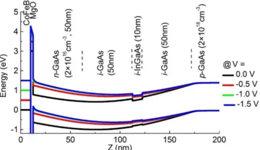
Following the experimental Spin-LED structure, we perform a simulation of energy band diagram of CoFeB|MgO|GaAs-InGaAs quantum wells hetero-structure with forward bias of 0V(black), -0.5V(red), -1V(green) and -1.5V(blue), as shown in Fig. 2. The thickness of each layer in the built simulation structure is the same as the thickness of grown sample; the donor concentration and acceptor concentration used in simulation are also the same with the real sample. The MgO layer here is modeled as an insulator with a very large bandgap and can block the flow of carriers between the GaAs-InGaAs quantum wells and the CoFeB as bias is applied. In addition, the band bending in the GaAs-InGaAs quantum wells is almost consistent. From the band diagram, the presence of an electrical forward bias can lift the Femi level of CoFeB(EF, CoFeB). In particular, EF, CoFeB reaches the conduction band edge when a forward bias of ~-1.5V is applied. It is found that the Schottky barrier height (EC-EF, CoFeB) and tunneling barrier height are dependent and they decrease with increase of forward bias.
Based on the understanding of the band diagram, we can discuss the transport behavior. Fig. 3 shows the semi-logarithmic forward and reverse current voltage characteristics of InGaAs/GaAs QW spin-LED measured from 20K to room temperature.When the negative bias is applied, for example as shown in Fig. 3(b), the LED is under p-i-n forward bias condition, with lower resistance compared with the resistance under reverse bias(when applying positive voltage). Obviously, the diodes show good rectifying behavior at all temperatures with the current showing an exponential increase in the forward bias and a weaker voltage dependence in the reverse bias. It is clear that the current through the diode
increased with increasing temperature from 20K to RT at fixed bias voltage, due to the increase of thermionic emission[21]-[22]. It can also be noted that the reverse saturation current increases with the increase of measuring temperature, which is attributed to higher contributions from the thermally generated minority carriers. In the following discussions, we will focus on the forward bias condition which gives radioactively right-or left-circularly polarized light,[11] where small current flows initially until the applied voltage exceeds the threshold voltage (VTH). After this, current rises steeply with the bias. This can be explained by the VTH being related with barrier heights of Schottky barrier and tunneling barrier, as shown in Fig. 4. We plotted Schottky barrier height and tunneling barrier height extracted from simulated energy band diagram. As bias is applied from 0V to -1.5V, the tunneling barrier height drops from 2.9 eV to 2.6 eV, and Schottky barrier height drops from 0.75 eV to 0 eV. Compared Fig. 4 (b-c) with Fig. 4(a), It can be found that the VTH is near to the bias, under which Schottky barrier height drops to zero. When the Femi level of CoFeB reaches the conduction band edge, the Schottky barrier height is zero and the carriers are injected into LED only through the tunneling barrier without being required to overcome the Schottky barrier height.
Threshold voltage is related with quality of insulator|semiconductor interface, due to the interfacial trapping states. Thus, we can discuss the annealing effect on threshold voltage, to understand the annealing effect on the interface. Fig. 5 shows temperature-dependent threshold voltage for the sputtering and MBE samples before annealing, and annealed at 200°C and annealed at 300°C, respectively. It can be seen that VTH for all the samples decreases with temperature due to the increase of thermionic emission. However, there is a big difference in the effect of annealing on VTH between sputtering samples (red) and MBE samples (blue). VTH of sputtering sample before annealing is much larger, and can be reduced by annealing. For example, the threshold voltage measured at low temperature 20K, VTH (before annealing)is 1.26V and VTH decreases to 1.11V(after annealing at 200°C) and 0.56V(after annealing at 300°C). However, there is no obvious annealing effect on VTH for MBE samples, VTH of MBE sample after annealing at 200°C and 300°C is approximately the same as that before annealing. Considering that VTH is near to the bias under which Schottky
barrier height drops to zero, we suggest that the annealing plays a role in reducing Schottky barrier height for sputtering samples but not MBE samples. It is known that the annealing can improve the crystallization and interfacial quality. Therefore, electrical injection and Schottky barrier height is related with MgO|GaAs-InGaAs interfacial sates.
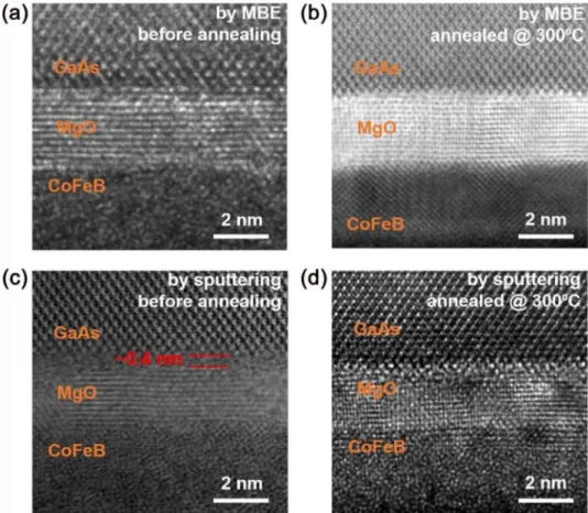
In order for us to have a clear understanding of the annealing on the interfacial structure, we performed the studies of interfacial morphological and crystallographic information by HR-TEM and HR-STEM, as shown in Fig. 6. Firstly, we compared the TEM images for MBE samples before annealing [Fig. 6(a)] and after annealing at 300 °C [Fig. 6(b)]. It is found that in both cases, the MgO|GaAs interface is sharp. Secondly, the presence of a thin amorphous layer (~0.4 nm) is detected at the MgO|GaAs interface (bottom interface) for the sputtering sample before annealing [Fig. 6(c)]This amorphous layer may play a role to induce interfacial states as discussed below. Finally, for the sputtering samples after 300°C annealing [Fig. 6(d)], full crystallization of CoFeB layer is also confirmed, same as the MBE sample. It is also noted that the amorphous layer at MgO|GaAs interface is much reduced after annealing. This study reveals that control of the MgO|GaAs interface is essential for an optimal effective injection. The MgO|GaAs can induce interfacial states which plays a role in modulating band-structure (Schottky barrier height) and VTH.
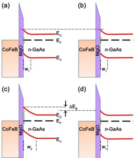
The difference of annealing effect on the band schematic diagram between sputtering sample and MBE sample is demonstrated as shown in Fig. 7. Due to the MgO|GaAs interface being sharp for MBE samples at both grown and annealed states, the interfacial states is thus similar for MBE samples by both grown and after annealing states, as shown in Fig. 7(a-b). However, as studied by TEM, a thin (~0.4nm) amorphous layer at the MgO|GaAs interface of sputtering sample with grown state, this interfacial amorphous layer will induce more defects which increases the interfacial trapping states, hence it can heighten( EB) and widen Schottky barrier(w2-w1). The amorphous layer in the grown sputtering samples can be improved and crystallized after annealing, therefore the Schottky barrier can be improved to be the same as that of MBE samples, as shown in Fig. 7 (c-d).
In summary, the interfacial morphological and crystallographic information of CoFeB|MgO|GaAs-InGaAs quantum wells hetero-structure with textured MgO tunnel barrier fabricated by two different techniques of sputtering and MBE has been studied. The MgO|GaAs interface is sharp in both cases of grown sates and annealing states for MBE sample. A thin amorphous layer (~0.4 nm) is observed at the MgO|GaAs interface for the sputtering sample before annealing, and it can be much reduced and improved after annealing. The amorphous layer in sputtering sample can play a role as interfacial trapping to heighten and widen Schottky barrier to influence electrical injection. Accordingly, for forward and reverse current voltage characteristics, it is found the threshold voltage decreases as the annealing temperature changes from room temperature to 300°C for sputtering sample. There is not much difference in threshold voltage with the annealing temperature for MBE sample. Our study suggests that the control of MgO|GaAs interface is essential for an optimal which play a role in modulating band-structure (Schottky barrier height) and VTH.
Our work has demonstrated that the CoFeB|MgO|GaAs interfaces are important and can be engineered thanks to the use of two types of growth for the textured MgO tunnel barriers, which ensures the efficient electrical injection.
Acknowledgments
This work is supported by the National Natural Science Foundation of China (No. 11674085), French National Research Agency (ANR) FEOrgSpin project, the joint ANR-National Natural Science Foundation of China (NSFC) ENSEMBLE project (Grant Nos. ANR-14-0028-01 and NNSFC 61411136001), and Technology Innovation Project of Guizhou Provincial Commission of Economy and Information Technology (No. 2017021).
References
[1] I. Zutic, J. Fabian, S. D. Sarma, Spintronics: Fundamentals and applications, Rev. Mod. Phys. 76 (2004) 323-410.
[2] A. Fert, Nobel Lecture: Origin, development, and future of spintronics, Rev. Mod. Phys. 80 (2008) 1517-1530.
[3] P. A. Grünberg, Nobel Lecture: From spin waves to giant magnetoresistance and beyond. Rev. Mod. Phys. 80 (2008) 1531-1540.
[4] S. Datta, B. Das, Electronic analog of the electro-optic modulator, Appl. Phys. Lett. 56 (1990) 665-667.
[5] M. Johnson, Spin injection in metals: The bipolar spin transistor, J. Magn. Magn. Mater. 156 (1996) 321-324.
[6] H. C. Koo, J. H. Kwon, J. Eom, J. Chang, S. H. Han, M. Johnson, Control of spin precession in a spin-injected field effect transistor, Science 325 (2009) 1515-1518. [7] S. Liang, H. Yang, P. Renucci, B. Tao, P. Laczkowski, S. Mc-Murtry, G. Wang, X.
Marie, J. George, S. Petit-Watelot, A. Djeffal, S. Mangin, H. Jaffrès, Y. Lu, Electrical spin injection and detection in molybdenum, Nat. Commun. 8 (2017) 14947.
[8] R. Fiederling, M. Keim, G. Reuscher, W. Ossau, G. Schmidt, A. Waag, L. W. Molenkamp, Injection and detection of a spin-polarized current in a light-emitting diode, Nature 402 (1999) 787-790.
[9] Y. Ohno, D. K. Young, B. Beschoten, F. Matsukura, H. Ohno, D. Awschalom, Electrical spin injection in a ferromagnetic semiconductor heterostructure, Nature 402 (1999) 790-792.
[10] M. Holub, P. Bhattacharya, Spin-polarized light-emitting diodes and lasers, J. Phys. D: Appl. Phys. 40 (2007) R179 R203.
[11] S. Liang, T. Zhang, P. Barate, J. Frougier, M. Vidal, P. Renucci, B. Xu, H. Jaffres,J. M. George, X. Devaux, M. Hehn, X. Marie, S. Mangin, H. Yang, A. Hallal, M. Chshiev, T. Amand, H. Liu, D. Liu, X. F. Han, Z. Wang, Y. Lu, Large and robust electrical spin injection into GaAs at zero magnetic field using an ultrathin CoFeB/MgO injector, Phys. Rev. B 90 (2014) 085310.
[12] F. Cadiz, A. Djeffal, L. Delphine, A. Balocchi, B. Tao, B. Xu, S. Liang, M. Stoffel, X. Devaux, H. Jaffres, J. M. George, M. Hehn, S. Mangin, H. Carrere, X. Marie, A. T. Thierry, X. F. Han, Z. Wang, B. Urbaszek, Y. Lu,P. Renucci, Electrical Initialization of Electron and Nuclear Spins in a Single Quantum Dot at Zero Magnetic Field, Nano Lett. 18 (2018) 2381-2386.
[13] B. Tao, P. Barate, X. Devaux, P. Renucci, J. Frougier, A. Djeffal, S. Liang, B. Xu, M. Hehn, H. Jaffrès, J. M. George, X. Marie, S. Mangin, X. Han, Z. Wang, Y. Lu, Atomic-scale understanding of high thermal stability of the Mo/CoFeB/MgO spin injector for spin-injection in remanence, Nanoscale 10 (2018) 10213-10220.
[14] T. Taniyama, E. Wada, M. Itoh,M. Yamaguchi, Electrical and optical spin injection in ferromagnet/semiconductor heterostructures, NPG Asia Mater. 3 (2011) 65 73.
[15] P. Barate,
with Different MgO Growth Processes, Phys. Rev. Appl. 8 (2017) 054027.
[16] P. Barate, S. Liang, T. T. Zhang, J. Frougier, M. Vidal, P. Renucci, X. Devaux, B. Xu, H. Jaffrès, J. M. George, X. Marie, M. Hehn, S. Mangin, Y. Zheng, T. Amand, B. Tao, X. F. Han, Z. Wang, Y. Lu, Electrical spin injection into InGaAs/GaAs quantum wells: A comparison between MgO tunnel barriers grown by sputtering and molecular beam epitaxy methods, Appl. Phys. Lett. 105 (2014) 012404.
[17] A. Fert, H. Jaffres, Conditions for efficient spin injection from a ferromagnetic metal into a semiconductor, Phys. Rev. B 64 (2001) 184420.
[18] X. Jiang, R. Wang, R. M. Shelby, R. M. Macfarlane, S. R. Bank, J. S. Harris, S. S. P. Parkin, Highly Spin-Polarized Room-Temperature Tunnel Injector for Semiconductor Spintronics using MgO(100), Phys. Rev. Lett. 94 (2005) 056601.
[19] G. L. Snider, I.-H. Tan, E. L. Hu, Electron states in mesa-etched one-dimensional quantum well wires, J. Appl. Phys. 68 (1990) 2849-2853.
[20] I-H. Tan, G. L. Snider, L. D. Chang, E. L. Hu, A self-consistent solution of Schrödinger Poisson equations using a nonuniform mesh, J. Appl. Phys. 68 (1990) 4071-4076.
[21] C. V. Prasad, M. S. P. Reddy, V. R. Reddy, C. Park, Effect of annealing on chemical, structural and electrical properties of Au/Gd2O3/n-GaN heterostructure with a high-k rare-earth oxide interlayer, Appl. Surf. Sci. 427 (2018) 670 677.
[22] M.
Gryglas-Balcerzak, M. Sawicki, D. Wasik, Magnetotransport investigations of (Ga,Mn)As/GaAs Esaki diodes under hydrostatic pressure, Appl. Surf. Sci. 396 (2017) 1875 1879.
Fig. 1. (a) Schematic device structure of spin-LED device. (b) Structure of the recombination active region consists of a single InGaAs/GaAs QW by MBE. CoFeB/MgO/GaAs spin injector layers are decomposed in terms of a top interface CoFeB/MgO and a bottom interface MgO/GaAs, in which CoFeB/Ta is prepared by sputtering and MgO is deposited by MBE or sputtering.
Fig. 3. Semi-logarithmic forward and reverse current voltage characteristics measured from 20K to room temperature, for InGaAs/GaAs QW spin-LED with sputtering grown MgO annealed at different temperatures (a-c), and MBE grown MgO annealed at different temperatures (d-f). VT indicates threshold voltage, for example as marked in (b).
Fig. 4. (a) Semi-logarithmic forward and reverse current voltage characteristics measured at 20K sputtering grown MgO annealed, VT is threshold voltage. (b) Schottky barrier height extracted from simulated energy band diagram. (c) Extracted tunneling barrier height.
Fig. 5. Temperature dependent threshold voltage, VT, for the samples with sputtering and MBE grown MgO annealed at different temperatures.
Fig. 6. (a) HR-TEM images of sample with MBE grown MgO before annealing. (b) HR-TEM image of the sample with MBE grown MgO after annealing at 300 °C. (c) HR-TEM images of sample with sputtered MgO before annealing, there is one amorphous MgO layer at MgO/GaAs interface with thickness of 0.4nm as indicated. (d) HRTEM image of the sample with sputtered MgO after annealing at 300 °C.
Fig. 7. (a-b)Schematic of band diagram for MBE grown MgO sample before annealing and after annealing, respectively. (c-d) Schematic of band diagram for sputtering grown MgO sample before annealing and after annealing, respectively.