10-nm Fin-width InGaSb p-channel self-aligned
FinFETs using antimonide-compatible digital etch
The MIT Faculty has made this article openly available. Please share
how this access benefits you. Your story matters.
Citation
Lu, W. et al. "10-nm Fin-width InGaSb p-channel self-aligned
FinFETs using antimonide-compatible digital etch." IEEE
International Electron Devices Meeting (IEDM), December 2017, San
Francisco, CA, USA, Institute of Electrical and Electronics Engineers
(IEEE), January 2018 © 2017 IEEE
As Published
http://dx.doi.org/10.1109/iedm.2017.8268412
Publisher
Institute of Electrical and Electronics Engineers (IEEE)
Version
Author's final manuscript
Citable link
https://hdl.handle.net/1721.1/126200
Terms of Use
Creative Commons Attribution-Noncommercial-Share Alike
10-nm Fin-Width InGaSb p-Channel Self-Aligned FinFETs
Using Antimonide-Compatible Digital Etch
W. Lu
1, I. P. Roh
2, D.-M. Geum
2, S.-H. Kim
2, J. D. Song
2, L. Kong
1, and J. A. del Alamo
11Microsystems Technology Laboratories, MIT, Cambridge, MA, USA, email: [email protected]
2Center for Opto-Electronic Materials and Devices, Korea Institute of Science and Technology, Seoul, South Korea
Abstract—We have fabricated self-aligned InGaSb p-channel
FinFETs using a novel antimonide-compatible digital etch. This is the first demonstration of digital etch on InGaSb-based transistors of any kind. It has enabled the first fabricated InGaSb FinFETs featuring fin widths down to 10 nm and gate lengths of 20 nm. Single fin transistors with Wf = 10 nm and
channel height of 23 nm (fin aspect ratio of 2.3) have achieved a record transconductance of 160 μS/μm at VDS = 0.5 V. When
normalized to device footprint, it reaches a record high gm =
704 μS/μm. Digital etch has been shown to effectively improve the turn-off characteristics of the devices.
I. INTRODUCTION
Among III-V compound semiconductors, antimonide-based compounds such as InGaSb are promising material candidates for logic and high frequency devices, optoelectronics, and ultra-low-power transistors such as TFETs [1-4]. For electronics, antimonides feature a high hole mobility that improves with the application of compressive stress [5]. This makes this family of materials of interest for p-channel MOSFETs for future CMOS applications. A few demonstrations of p-type planar, fin, and nanowire MOSFETs have been published [6-12]. Nevertheless, progress in antimonide-based electronics has been slow. This can be partly explained by the challenging materials aspects of epitaxial growth and device fabrication due to the reactive nature of antimony-containing compounds.
In this work, we greatly advance the state-of-the-art of antimonide-based electronics by demonstrating deeply-scaled InGaSb p-channel FinFETs through a fully CMOS-compatible fabrication process. To achieve this, we have developed a new Sb-compatible digital etch which is controllable and benign, and we have perfected Ni ohmic contacts and fin RIE. We demonstrate the first InGaSb p-channel FinFETs with fin widths down to 10 nm and gate lengths down to 20 nm. These devices display record electrical characteristics.
II. ANTIMONIDE-COMPATIBLE DIGITAL ETCH
One of the most critical challenges of InGaSb 3D device fabrication is the difficulty of performing digital etch (DE), a key process step in Si and InGaAs deeply scaled devices. DE is a process technique that separates the oxidation and oxide removal elements of conventional chemical etching enabling self-limiting nm-scale control. DE is essential to achieve devices with critical dimensions in the sub-10 nm range and also to remove RIE damage and passivate the fin/nanowire surface. Conventional DE using acids dissolved in water fails with antimonides due to their high reactivity. In a recent work [13], we demonstrated the first digital etch of InGaSb using oxygen plasma combined with HCl dissolved in alcohol. However, when attempting to make devices, we identified one
important deficiency in this technique and that is material selectivity. Typical InGaSb-based devices include layers of arsenides and often contain aluminum compounds. It is very problematic if the DE etch rate shows a strong dependence on the different materials encountered in a device. This is unfortunately the case for the DE technique of antimonides.
Fig. 1 illustrates an InAs/InGaSb/AlGaSb nanowire.
Alcohol-based DE produces an initial radial etch rate on the III-Sb of 1.0 nm/cycle, while the etch rate on the InAs portion of the nanowire is about 2.0 nm/cycle. To complicate matters, after 10 cycles, the average etch rate of the III-Sb portion of the structure is drastically reduced to about 0.21 nm/cycle, while all the InAs has already been etched away. Other authors have reported a similar much reduced etch rate of GaSb in water-based digital etch [3].
The issue lies in the oxidation properties of antimonides. For GaSb, strong oxidizing agents, like hydrogen peroxide, produce Sb2O5 in addition to Ga2O3, Sb2O3 and elemental Sb.
Sb2O5 is insoluble in most acids or alkali [14]. Therefore, when
enough Sb2O5 has been formed on the surface, digital etch
stops. To address this issue, we have investigated digital etch by multiple combinations of oxidation and etch methods (Fig.
2). In the end, our study reveals that 3 min exposure in pure O2
chamber at RT combined with 10% HCl:IPA etch for 30 s gives satisfactory results. Fig. 3 shows the new DE process in action in the same heterostructure as in Fig. 1. A consistent radial etching rate of 2.0 nm/cycle for both InAs, InGaSb and AlGaSb is demonstrated. An issue worth noting is that AlGaSb is attacked and roughened after multiple cycles of DE, as shown in Fig. 3(d). Addressing this will require further studies.
III. INGASB FINFETFABRICATION
Fig. 4 shows the heterostructure utilized in this work. It is
grown by MBE on (100) S.I. GaAs substrate. It features an In0.25Ga0.75Sb channel with a thickness (Hc) of 23 nm. The
buffer is Al0.97Ga0.03Sb for high resistivity, with 50 nm
liner-graded to Al0.8Ga0.2Sb for reduced rate of oxidation when
exposed, and also to yield a smooth channel interface. The p+
cap features a composite InAs/InAsSb design [15] with a doping level of 3·1019 cm-3. There is a Be delta-doping layer
with 5·1011 cm-2 located 5 nm below the channel. Fig. 5 shows
the AFM and TEM cross-section measurements of the grown wafer. The surface mean roughness of the entire heterostructure and the Al0.8Ga0.2Sb buffer surface is 1.29 nm
and 0.65 nm, respectively. The interfaces are atomically smooth. Fig. 6 summarizes key parameters of the grown wafer. The hole mobility is 1175 cm2/V·s. The buffer layer has high
resistivity of 4.3·106 Ω·cm. From XRD, the InGaSb channel is
Fig. 7 outlines the process flow for FinFET fabrication, and Fig. 8 sketches final device cross-sections along and across the
fin direction. First, the ohmic contact pattern is defined by e-beam lithography, and then Ni is e-e-beam evaporated and lifted off. The Ni contacts are then covered by a CVD SiO2 spacer.
The gate foot is next defined by EBL, followed by mesa photolithography and mesa SiO2 RIE. The gate recess consists
of two steps. The first 30 nm of the 35 nm p+ cap are removed
by timed Cl2/N2 dry etch. The rest is selectively etched in 10:1
citric acid:H2O2. This yields an undercut of the p+cap that is
less than 20 nm, while maintaining a smooth top surface. Fins are then patterned and RIE-etched using HSQ as the mask. Right after RIE, 1 cycle of the antimonide-compatible DE process described above is performed, followed by 3.5 nm ALD Al2O3 gate dielectric at 175°C. 60 nm of Al is sputtered
as gate metal, and the gate head is defined by Ti/Au patterning and Al RIE. Finally, 30 nm of SiO2 spacer is deposited and
pads are formed following via photolithography and etching. The process results in a gate that is self-aligned to the p+ cap.
The HSQ fin mask remains till the end of the process, resulting in a double-gate FinFET structure. The Ni ohmic contact is unintentionally alloyed during the backend CVD step at 300°C.
Devices with Lg ranging between 20 nm and 1 µm and Wf
between 10 nm and 100 nm were fabricated. The chip contained single-fin transistors as well as arrays with 25, 50, or 100 fins in parallel.
Fig. 9 illustrates the fin etch technology developed in this
process which represents an improvement over what was demonstrated before [7]. The test structure comprises of 50 nm InAs on GaSb. RIE was performed by ICP BCl3/Ar/SiCl4
plasma at 250°C, 280 W RF platen power and 20 W ICP power. Smooth and vertical sidewalls are obtained with a fin width down to 15 nm, a marked improvement over [7] where the InAs layer was roughened during dry etch. Here, simultaneous etching of antimonides and arsenides is achieved without roughening any of the surfaces.
Fig. 10 shows ohmic contact resistance, measured by
circular TLM test structures on the heterostructure in Fig. 4. The inset shows Rc obtained by Mo, W, and Ni contacts as a
function of annealing temperature. Ni ohmic contacts annealed at 350°C for 3 min yield a record contact resistance of 22.3 Ω·μm, which corresponds to an ultra-low contact resistivity of 4.6·10-9 Ω·cm2. This Rc is a factor of 4X better
than our earlier demonstration [15] and it arises from the use of a composite p+ cap design and a higher doping level (3·1019
vs. 1·1019 cm-3 in [15]).
Fig. 11 shows an SEM image of a finished device. Fig. 12
shows TEM cross sections of the fin structure of a completed device demonstrating a fin width of 10 nm, fin height of 115 nm and a channel aspect ratio (AR = Hc/Wf) of 2.3. The fin
sidewall angle is 84° and the fin pitch is 100 nm.
IV. RESULTS
Fig. 13 shows the electrical characteristics of the most
aggressively scaled InGaSb single-fin MOSFET with Wf = 10 nm and Lg = 20 nm. A peak gm = 160 μS/μm and a
lowest Slin = 260 mV/dec are obtained. Characteristics of a 100
fin array device with Wf = 10 nm and Lg = 1 μm are displayed
in Fig. 14, showing good saturation behavior. Unless indicated otherwise, all the FOMs are normalized by the total conducting periphery of the gate (2Hc·Nf).
Scaling behavior of our devices is shown in Fig. 15 and 16. Maximum transconductance extracted at VDS = -0.5 V shows
well-behaved dependence on Lg and Wf. VT extracted at
VDS = -50 mV shows mitigated VT rolloff with fin-width
scaling. Figs. 17-18 shows the measurement of Ron (at
VGS = -1 V), and extraction of fin resistance Rf and access
resistance RSD. The expected scaling behavior of Rf and RSD as
~1/Wf is observed.
The demonstrated devices, even at long channel, show insufficient turn-off characteristics. Nevertheless, the results here represent a significant improvement over earlier InGaSb FinFETs [6] due to the new DE technique. To illustrate its role,
Fig. 19(a) shows the impact of DE on the subthreshold
characteristics of otherwise identical transistors. Without DE, turn-off is very poor. A single DE cycle yields a drastic improvement with the residual current dropping more than two decades. This illustrates the ability of DE to reduce sidewall RIE damage. Additional cycles of DE worsen the off-state behavior. This could be attributed to the fact that AlGaSb buffer is easily oxidized and damaged, especially during the oxidation process of DE, consistent with what we observed in Fig. 3(d). The residual off-state current that is left after 1 DE cycle in Fig. 19(a) is due to buffer leakage. This is shown in Fig. 19(b) that shows the subthreshold characteristics of long-channel devices with fin width ranging from 100 nm to 14 nm. All devices were treated with 1 DE cycle. Below a fin width of 22 nm, the turn-off behavior remains unchanged. Test devices with no InGaSb channel but gated AlGaSb fins show that there is a residual leakage path underneath the channel which is responsible for the improper off-state behavior. This is likely due to the etched and exposed AlGaSb buffer which is easier to be oxidized than InGaSb forming a surface conduction leakage path. Alleviating this will require structural device innovations, such as lateral suspended or vertical device structures.
Fig. 20 benchmarks gm vs. Wf among published InGaSb
p-MOSFETs, normalized in two ways. When normalized by the conducting gate periphery, as in Fig. 20(a), a record gm of
268 μS/μm is exhibited at Wf = 46 nm and VDS = 0.5 V. The
maximum gm drops as Wf decreases, as in InGaAs FinFETs
[16]. When gm is normalized by the footprint of the fin, as is
relevant for high-density FinFETs, the 10 nm fin width devices demonstrate a high gm/Wf = 704 μS/μm (Fig. 20(b)).
V. CONCLUSIONS
Highly scaled InGaSb p-channel FinFETs with smallest fin width of 10 nm, fin AR > 2 and Lg=20 nm are demonstrated for
the first time. These results are enabled by a new antimonide-compatible digital etch technique. Record results are demonstrated across a broad range of Wf and Lg. This work not
only highlights the potential of InGaSb p-channel multigate MOSFETs, but also pushes significantly the state-of-the-art of antimonide fabrication technology for general applications in which the antimonide-based compounds can shine.
Fig. 1. (a) InAs/InGaSb/AlGaSb vertical nanowire after RIE with initial
diameter of 25 nm, and after (b) 3 cycles and (c) 10 cycles of digital etch in O2 plasma and HCl:IPA. Noted are the average radial etch rates of the
InGaSb/AlGaSb portion of the nanowires.
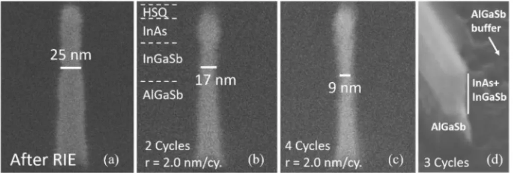
Fig. 3. (a) InAs/InGaSb/AlGaSb vertical nanowire after RIE with initial diameter of 25 nm,
and after (b) 2 cycles, and (c) 4 cycles of digital etch in O2 atmosphere and HCl:IPA showing
stable and uniform etching rate. (d) Fin structure after 3 cycles of DE showing non-uniform sidewall and surface etching of the AlGaSb portion of the structure.
Fig. 2. A survey of digital etch techniques tested, by combining
various oxidation methods and oxide etch solutions. Those marked in blue gave the best results.
Fig. 4. Starting heterostructure for InGaSb
p-channel FinFET fabrication. • HCl clean, Ni ohmic contact • CVD SiO2 contact spacer
• Gate EBL, SiO2 dry etch
• Mesa photo, SiO2 dry etch
• Gate recess I: p+ cap timed RIE • Gate recess II: p+ cap selective wet etch • Fin EBL, BCl3/Ar/SiCl4 dry etch
• Antimonide-compatible digital etch • ALD Al2O3 gate dielectric, 175 °C
• Al gate sputtering
• Gate head photo and patterning • CVD SiO2, via photo and RIE
• Pad formation
Fig. 5. AFM image of (a) as-grown MBE
heterostructure and (b) of the surface of the graded buffer structure. (c) TEM lattice image of the channel and spacer region of the heterostructure.
Fig. 6. Summary of electrical
properties of the InGaSb
heterostructure. Fig. 7. Process flow for InGaSb FinFETs.
Fig. 8. Schematic of FinFET cross-sections (a) along the fin and (b) across the fin. Fig. 9. SEM micrographs of RIE-etched InAs/GaSb fins following the recipe of (a) [7], and (b), (c) this work.
Acknowledgement: This work is sponsored in part by SRC (#2016-LM-2655), DTRA (#HDTRA1-14-1-0057), KIST, and Lam Research. Devices
fabrication was performed at the Microsystems Technology Laboratories and SEBL at MIT. The KIST authors acknowledge partial support from the KIST institutional program.
References: [1] B. R. Bennett et al., Solid State Electron, v. 49, 2005. [2] P. S. Dutta, and H. L. Bhat, J. Appl. Phys, v. 81, p. 5821, 1997. [3] E. Memisevic
et al., IEDM, pp. 19.1.1, 2016. [4] D. Cutaia et al., VLSI, 2016. [5] L. Guo et al., EDL, v. 35, no. 11, p.1088, 2014. [6] A. S. Babadi et al., Appl. Phys. Lett., v. 110, no. 5, 2017. [7] W. Lu et al., IEDM, p.31.6.1, 2015. [8] K. Nishi et al., VLSI, 2015. [9] K.-H. Goh et al., IEDM, p.15.4.1, 2015. [10] R. L. Chu et al., APL, 2014. [11] A. Dey et al., Nano Lett., vol. 12, p.5593, 2012. [12] A. Nainani et al., IEDM, p.6.4.1, 2010. [13] W. Lu et al., EDL, vol. 38, no. 5, p. 548, 2017. [14] Z. Liu et al., JVST B., vol. 21, no. 1, p. 2587, 2003. [15] L. Guo et al., EDL, vol. 36, no. 6, p.546, 2015 [16] A. Vardi and J. A. del Alamo, EDL, v. 37, no. 9, p. 1104, 2016.
Fig. 10. Ni ohmic contact resistance on this
heterostructure. Inset: Rc benchmark of Mo, W
and Ni ohmic contacts and earlier results [15].
Fig. 11. SEM image of a
finished InGaSb FinFET.
Fig. 12. HR-TEM images of finished InGaSb FinFET with fin
width of 10 nm, fin aspect ratio of 2.3, and 3.5 nm Al2O3 gate
dielectric.
Fig. 13. (a) Output characteristics of InGaSb single-fin device with Wf =
10 nm, Lg = 20 nm; (b) subthreshold characteristics of the device. Inset:
transconductance characteristics of the device, with peak gm = 160 μS/μm.
Fig. 14 (a) Output characteristics of InGaSb long channel array FinFET
with Wf = 10 nm, Lg = 1 μm, Nf = 100; (b) subthreshold characteristics of
the device. Inset: transconductance characteristics of the device.
Fig. 15. Impact of Wf and Lg scaling
on maximum gm at VDS = -0.5 V.
Fig. 16. Impact of Wf and Lg scaling
on VT at VDS = -50 mV.
Fig. 17. ON resistance of devices with
various Wf at VGS = -1 V.
Fig. 18. Extracted (a) fin sheet resistance vs.
fin width, and (b) access resistance vs. fin width.
Fig. 19. (a) Subthreshold characteristics of FinFETs with the same final
Wf = 20 nm, after 0, 1, and 4 digital etch cycles. (b) Subthreshold
characteristics of FETs with various Wf and Lg = 1 μm, and test device
with identical geometry but no InGaSb channel (1DE cycle in all).
Fig. 20. Benchmark of maximum gm vs. Wf for InGaSb FinFETs
and planar MOSFETs. (a) gm is normalized to the total
conducting periphery. (b) gm is normalized by fin footprint. The