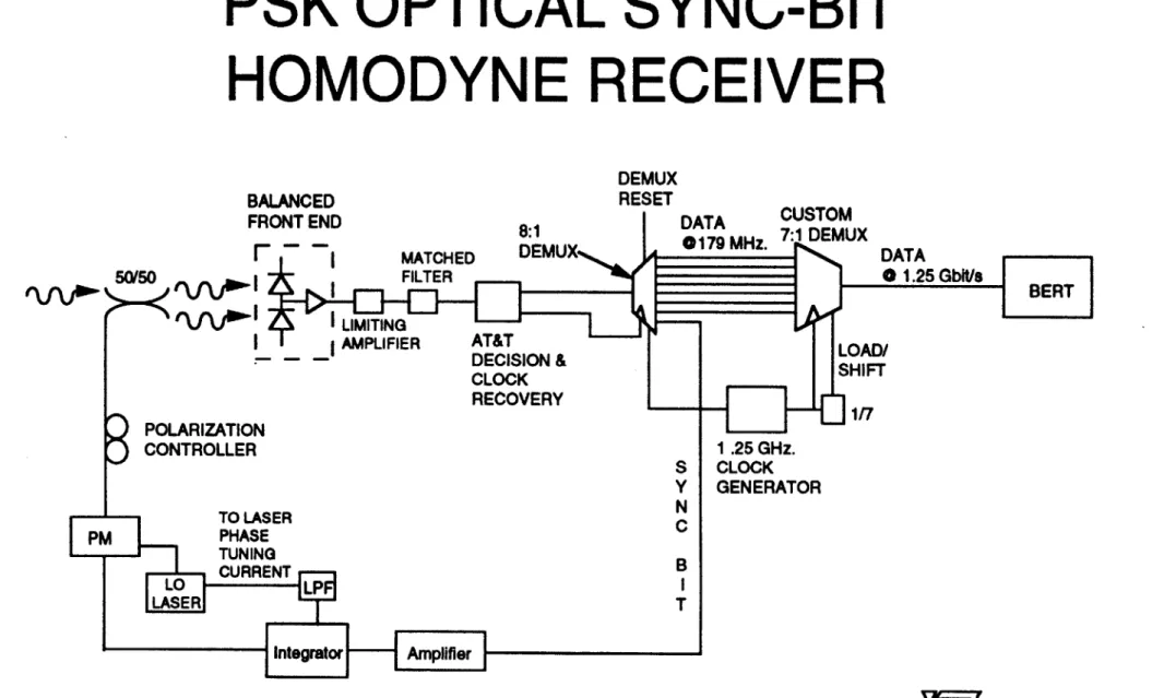
A 1.25 gigabit per second binary-phase-shift-keyed optical homodyne receiver
Texte intégral
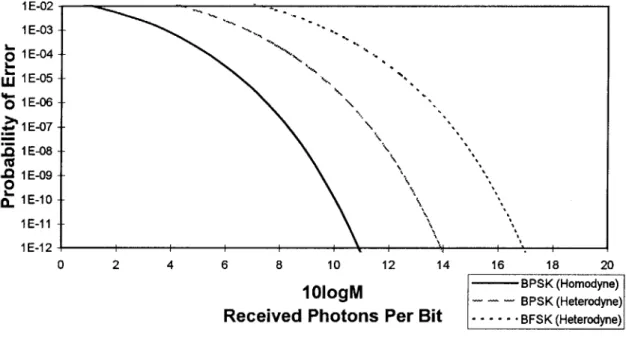
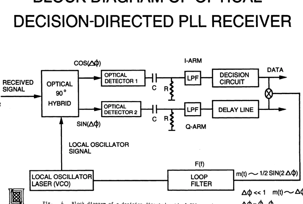
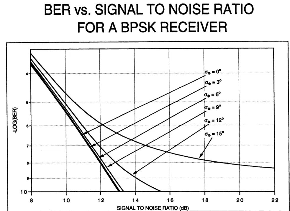
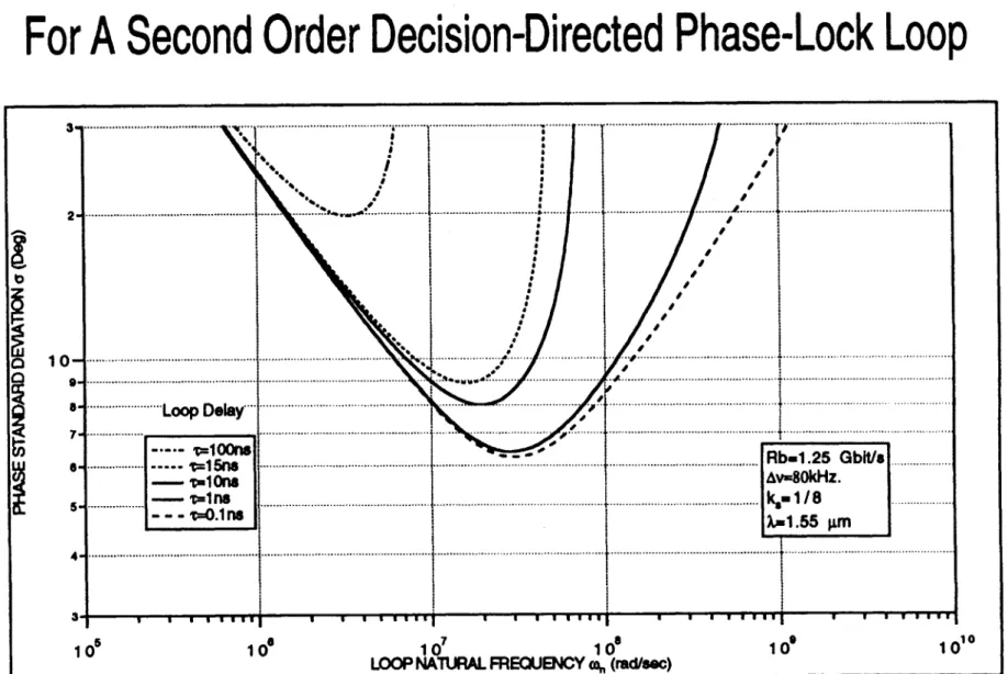
Figure


Documents relatifs
Based on the above-mentioned studies, one could have expected no positive effect on strength from such a short duration program; yet, in the current study, the total work (sum of reps
The Canadian Task Force on Preventive Health Care recommends screening adults 60 to 74 years of age for colorectal cancer (strong recommendation), but given the severe
• Shared decision making is most relevant when there is a close trade-off between the harms and the benefits of a screening decision that could be altered by individual
Previous research work has developed tools that provide users with more effective notice and choice [9, 18, 19, 31]. With increasing concerns about privacy because of AI, some
The social intuitionist model of reasoning, which has greatly influenced the emotional approach states that moral and political rea- soning is effectively a process of
The assessment of the interactions of radionuclides with stable pollutant was carried out using ANOVA to test for significant differences between reference and stable
In fact, the absence of state variables and the hypothesis of independence between the risk over wage rates and risks existing in the training process, and also the assumption
Apart from discrete groups and duals of compact groups, the first test examples for a quantum Property RD should be the free quantum groups introduced by Wang [6], which are
