HAL Id: cea-01369277
https://hal-cea.archives-ouvertes.fr/cea-01369277
Submitted on 20 Sep 2016
HAL is a multi-disciplinary open access
archive for the deposit and dissemination of
sci-entific research documents, whether they are
pub-lished or not. The documents may come from
teaching and research institutions in France or
abroad, or from public or private research centers.
L’archive ouverte pluridisciplinaire HAL, est
destinée au dépôt et à la diffusion de documents
scientifiques de niveau recherche, publiés ou non,
émanant des établissements d’enseignement et de
recherche français ou étrangers, des laboratoires
publics ou privés.
Spin electronic magnetic sensor based on functional
oxides for medical imaging
Aurélie Solignac, Georg Kurij, Ruben Guerrero, Guillaume Agnus, Thomas
Maroutian, Claude Fermon, Myriam Pannetier-Lecoeur, Philippe Lecoeur
To cite this version:
Aurélie Solignac, Georg Kurij, Ruben Guerrero, Guillaume Agnus, Thomas Maroutian, et al.. Spin
electronic magnetic sensor based on functional oxides for medical imaging . SPIE Proceedings Series,
2015, 9551, pp.95512F. �10.1117/12.2188251�. �cea-01369277�
Spin electronic magnetic sensor based on functional oxides for medical
imaging
A. Solignac
*a, G. Kurij
b, R. Guerrero
a, G. Agnus
b, T. Maroutian
b, C. Fermon
a, M.
Pannetier-Lecoeur
a, Ph. Lecoeur
ba
DSM/IRAMIS/SPEC, CNRS UMR 3680, CEA Saclay, 91191 Gif sur Yvette, France
b
Université Paris Sud, CNRS UMR 8622, Inst. Elect. Fondamentale, 91405 Orsay, France
ABSTRACT
To detect magnetic signals coming from the body, in particular those produced by the electrical activity of the heart or of the brain, the development of ultrasensitive sensors is required. In this regard, magnetoresistive sensors, stemming from spin electronics, are very promising devices. For example, tunnel magnetoresistance (TMR) junctions based on MgO tunnel barrier have a high sensitivity. Nevertheless, TMR also often have high level of noise. Full spin polarized materials like manganite La0.67Sr0.33MnO3 (LSMO) are attractive alternative candidates to develop such sensors because LSMO exhibits a very low 1/f noise when grown on single crystals, and a TMR response has been observed with values up to 2000%. This kind of tunnel junctions, when combined with a high Tc superconductor loop, opens up possibilities to develop full oxide structures working at liquid nitrogen temperature and suitable for medical imaging. In this work, we investigated on LSMO-based tunnel junctions the parameters controlling the overall system performances, including not only the TMR ratio, but also the pinning of the reference layer and the noise floor. We especially focused on studying the effects of the quality of the barrier, the interface and the electrode, by playing with materials and growth conditions.
Keywords: Spin electronic, magnetic sensors, magnetic tunnel junction, functional oxides, interface engineering
1. INTRODUCTION
Magnetic tunnel junctions (MTJ), consisting of two ferromagnetic electrodes separated by an insulating barrier, are one of the most promising devices for magnetic sensing purposes. However their high sensitivity is counterbalanced by a high level of noise, thus leaving the noise floor of the magnetic field sensors at the same level than other magnetoresistive devices [1]. Several routes have been proposed to enhance the signal to noise ratio in such a case, most of them reducing the low frequency noise in MTJs [2,3]. However another way to improve the performances is to increase the tunneling magnetoresistance (TMR) ratio by using other kinds of materials.
A good example of such an approach is the use of manganites as ferromagnetic electrodes instead of metallic ferromagnets. These materials exhibit a half metallic character, i.e. only one spin direction is present at the Fermi level, thus they exhibit a high TMR up to 2000% at low bias and at low temperatures [4-7]. Moreover, manganites are part of the family of perovskite oxides possessing a large range of physical properties, which can be combined in epitaxial heterostructures to develop high performance devices. One example is mixed sensors which are ultrasensitive magnetic sensors targeted at the detection of biomagnetic signals such as neuronal signals [8]. The use of oxides is expected to improve the performances of these sensors at 77K. Indeed they will combine the gain induced by an YBaCuO superconductor flux-to-field transformer and the high magnetoresistance of a La0.7Sr0.3MnO3 (LSMO) half metal-based MTJ’s.
Nevertheless, we, as other authors in literature, do not reproduce the highest TMR ratios in LSMO-based tunnel junctions. The electrode/barrier interface has been shown to be primordial in MTJ and especially several effects could appear at the LSMO/barrier side, for example the presence of dead layer (magnetic and in transport), different terminations or oxygen vacancies [9-11] which disturb the ideal interface. We present, in this paper, a systematic investigation of these effects and their impact on the TMR ratio by playing with the quality of the barrier, the interface and the electrode, thanks to a change of materials and growth conditions of the different MTJ layers.
2. SAMPLE PREPARATION
The MTJ stacks are deposited on a SrTiO3(100) substrate, with a nominal miscut lower than 0.1°, and a chemically and thermally treated surface at 900°C under pure oxygen in order to ensure a single TiO2 termination [12]. The stacking sequence and thicknesses are identical for all the junctions grown and studied in this paper. They are comprised of a SrTiO3 (STO) insulating barrier and have the following structure: La0.7Sr0.3Mn0.995Ru0.005O3 (LSMRO) (20nm) /LSMO (10nm) /STO (3nm) /LSMO (30nm) // STO. The Ru doping in the LSMRO layer increases its coercivity so that it plays the role of a hard layer in the MTJ [13]. A 10 nm thick LSMO layer is maintained between LSMRO and STO to have a better interface. In order to determine the key parameters for the junction properties, we have grown junctions under different conditions and with different materials. The samples and their growth conditions are listed in Table 1. For each sample, one parameter is changed compared to the reference sample grown with “standard” conditions. This reference sample has been fully characterized and possesses properties similar to the ones presented in Ref. [14].
Table 1: Summary of the growth conditions for all the samples: name, stack, growth temperature, O2 pressure during and after the
growth. The parameters in red and italic are modified compared to the standard growth conditions used for the PLD1350 highlighted in bold. The thicknesses of the junctions are identical: LSMRO (20nm) /LSMO (10nm) /Barrier (3nm) /LSMO (30nm) // substrate. The type of target used for STO is indicated into brackets: monocrystalline “STO(mono)” or sintered “STO(sintered)”.
N° Junction composition Growth temperature
O2 pressure during the growth
O2 pressure after the growth PLD1350 LSMRO/LSMO/STO(mono)/LSMO
STO(100) substrate 585°C 120 mTorr 300 Torr PLD1348 LSMRO/LSMO/STO(mono)/LSMO STO(100) substrate 585°C 1.5.10-2 mTorr (STO) 120 mTorr (other) 1h at 500° under 300 Torr PLD1349 LSMRO/LSMO/LAO/LSMO
STO(100) substrate 585°C 2.2.10-4 mTorr (STO) 120 mTorr (other) 1h at 500° under 300 Torr PLD1351 LSMRO/LSMO/STO(mono)/LSMO STO(100) substrate 585°C 250mTorr (LSMO)
120 mTorr (other) 300 Torr PLD1353 LSMRO/LSMO/STO(mono)/LSMO
STO(100) substrate 550°C 120 mTorr 300 Torr PLD1354 LSMRO/LSMO/STO(mono)/LSMO
STO(110) substrate 585°C 120 mTorr 300 Torr
PLD1355 LSMRO/LSMO/STO(sintered)/LSMO
STO(100) substrate 550°C 120 mTorr 300 Torr
With this serie of junctions, we wanted to test the effects of:
- The interface with the barrier, by replacing the STO with LaAlO3 (LAO) and by using an STO(110) oriented substrate. The corresponding junctions should possess a reduced dead layer at the interface between the barrier and the electrode [15].
- The barrier quality by doing a growth of the STO barrier under lower O2 pressure followed by an annealing under oxygen. These growth conditions are the optimal conditions for the STO in our PLD system. The second possibility is to use a crystalline STO target instead of the sintered STO target, so as to have a better STO layer [16]. The monocrystalline STO target is a STO substrate of 30mm diameter (Crystec).
- The quality of the LSMO electrodes by growing them under higher O2 pressure and at lower temperature. All the different stacks are grown by pulsed laser deposition with a KrF laser (248 nm wavelength) operated at 2 Hz repetition rate with a fluence of 3J/cm2. Deposition rates of 0.13ML/s for the LSMO and the LSMRO, and 0.39ML/s for the STO layer are obtained by tuning an attenuator on the beam path. A homogenizer ensures a top hat profile of the laser beam on the target. The full stack is grown under 120mTorr of oxygen at 585°C. At the end of the deposition process, the chamber is filled with oxygen up to 300mTorr for 10 minutes before the cooling down step. In order to control the deposition rate a thickness calibration is performed with single layers measured by X-Ray reflectivity. During the deposition of the stack all the conditions are kept as in the mentioned calibration step in order to deposit the desired thicknesses.
After preliminary characterizations using Atomic Force Microscope (AFM), and Superconducting Quantum Interference Device (SQUID) magnetometry, the samples are patterned with a standard optical lithography process into 10x10 µm2 square junctions for magneto-transport measurements. Following top electrode fabrication, the bottom electrode is etched by Ar ion milling. To control the etching, a secondary ion mass spectrometer (SIMS) is used and allows stopping the etching especially before the STO barrier during the first step. An additional STO barrier etching is necessary to access to the bottom electrode contact. The contact pads are defined by a 100nm thick palladium layer deposited by sputtering. After microfabrication, two junctions of 10 x 10 µm2 are measured on each sample to verify the reproducibility and uniformity of the sample. The resistance area product (RA) was in the range of 0.1-10MΩµm2 for all junctions.
Figure 1. Picture of a processed 10x10µm² junction. The light green part is the bottom electrode, the red crosshatched square is the top electrode and the light blue shapes are the Pd contacts.
3. PRELIMINARY CHARACTERIZATIONS
Preliminary characterizations are preformed to verify the magnetic and structural properties.
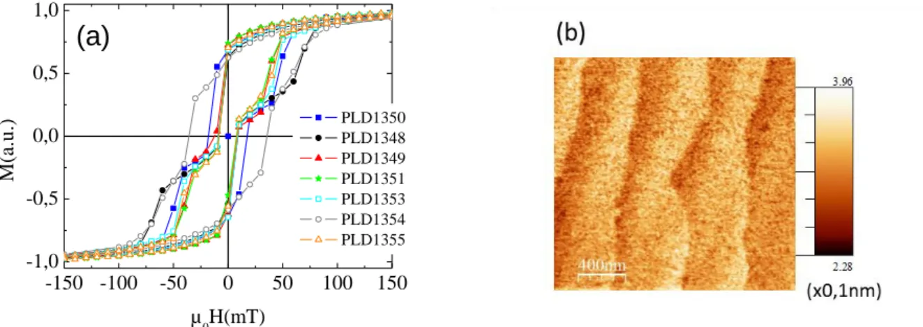
The hysteresis cycles, measured at low temperature on the stacks described in Table 1 and presented in Fig. 2 (a), are characteristic of the presence of two magnetic layers with two different coercive fields. The LSMRO/LSMO bilayer possesses a higher coercive field than the LSMO bottom electrode and thus switches at higher field. The coercive fields are similar for all the junctions with some fluctuations, around 50 mT (LSMRO/LSMO) and 10 mT (LSMO), except for the junction grown on top of STO(110) (PLD1354).
AFM images are taken on the top LSMRO surface of all the junctions after growth and are similar to the one presented in Fig. 2 (b). The atomic steps coming from the slight vicinality of the STO substrates (mean terrace widths 250-400 nm) are visible on top of all the junctions and the roughness on the terraces is lower than 0.2nm, i.e. half a LSMO unit cell. The only exception is the junction PLD1354 grown on STO(110), which has a surface roughness of 1.3nm.
-150 -100 -50 0 50 100 150 -1,0 -0,5 0,0 0,5 1,0 M (a.u .) µ 0H(mT) PLD1350 PLD1348 PLD1349 PLD1351 PLD1353 PLD1354 PLD1355
(a)
Figure 2. (a) Hysteresis cycles measured by SQUID magnetometry at 10K on the as grown stack described in Table 1. Two magnetization switches are observed and correspond to the coercive fields of the two electrodes of the junctions. (b) Typical AFM image 2x2µm² observed on top of the junctions after growth. The steps coming from the vicinal substrate are reproduced on top of the junction, which is characteristic of a layer-by-layer smooth growth mode. The rms (root mean square) roughness is lower than 0.2nm.
4. TUNNELING MAGNETORESISTANCE
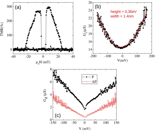
The transport measurements are performed after microfabrication in four point configuration (Fig. 1). The junctions are biased using a commercial current source and the voltage is sent to a set of homemade low noise amplifiers, the output being sent to a voltage acquisition card. The studied samples are cooled down in a He4 cryostat that contains also a superconducting coil in order to record the magnetoresistance curves and the current voltage curves at different magnetic fields. -40 -20 0 20 40 0 100 200 300 TM R(%) µ0H (mT)
(a)
-200 -100 0 100 200 14 16 18 20 22 24 26 height = 0,36eV width = 1.4nm(b)
Gd (µS ) V(mV) -1500 -100 -50 0 50 100 150 2 4 6 8 G d (µS) V (mV) P AP(c)
Figure 3. Measurements performed on a 10x10 µm2 junction of the PLD 1355 sample. (a) TMR versus magnetic field measured at 5K with 0.1nA bias current. (b) Dynamical conductance Gd=dI/dV measured at 300K. The red line is the simulation based on the Brinkman model [17]. The fitting parameters are the height and the width of the junctions. (c) Dynamical conductance Gd=dI/dV measured at 5K in the parallel (black squares) and antiparallel (red circles) states; the parallel and antiparallel states are different because a TMR effect is present at 5K contrary than at 300K.
First, the TMR ratio of the junction is measured, because it is a primordial parameter in MTJ. As example, Fig. 3 shows typical magnetoresistance measurements obtained at low temperature. We define the TMR ratio by
P P
AP R R
R
TMR(%)100( )/ , where RAP and RP are the antiparallel and parallel resistance respectively. In order to extract information on the quality of the barrier we performed other characterizations, especially I(V) characteristics at 300K and at 5K. At 300K (Fig. 3b), a simulation using a Brinkman [17] fit is realized, to extract the height and the width of the barrier. The estimated barrier height varies from 0.2 to 0.8eV between the different junctions (Table 1), which is much smaller than the value of the band gap in STO [18] but also slightly higher than values published for this type of junctions [5]. The width is also smaller than the real STO layer thickness. These two parameters are strongly dependent on the quality of the barrier and a possible explanation of their observed reduction is the decrease of the STO quality inside the barrier compared to bulk material. Impurities could be present in the barrier, such as oxygen vacancies. The
conductance at 5K (Fig. 3c) is no more parabolic as a function of the voltage and a strong drop of the conductance also called “zero bias anomaly” (ZBA) is observed at zero bias and is estimated at 5K byZBA(G100mV G0mV)/G0mV .
This ZBA has been attributed to the presence of metallic impurities in the barrier or at the interface with the electrodes which induce additional conduction channels [19] or a Coulomb gap [20]. A magnetic and transport dead layer in the LSMO at the interface with the STO creating an extra barrier may also be responsible for the ZBA. The effect of this double barrier disappears when the voltage increases. Thus a reduced ZBA will be characteristic of a better quality of the interface or of the barrier.
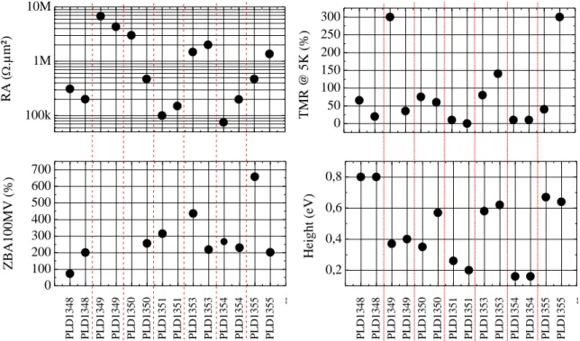
All the measurement curves are not shown in this paper but the key results are summarized in Fig. 4 for all the junctions (Table 1). 100k 1M 10M 0 50 100 150 200 250 300 P L D 1 3 4 8 P L D 1 3 4 8 P L D 1 3 4 9 P L D 1 3 4 9 P L D 1 3 5 0 P L D 1 3 5 0 P L D 1 3 5 1 P L D 1 3 5 1 P L D 1 3 5 3 P L D 1 3 5 3 P L D 1 3 5 4 P L D 1 3 5 4 P L D 1 3 5 5 P L D 1 3 5 5 --0 100 200 300 400 500 600 700 P L D 1 3 4 8 P L D 1 3 4 8 P L D 1 3 4 9 P L D 1 3 4 9 P L D 1 3 5 0 P L D 1 3 5 0 P L D 1 3 5 1 P L D 1 3 5 1 P L D 1 3 5 3 P L D 1 3 5 3 P L D 1 3 5 4 P L D 1 3 5 4 P L D 1 3 5 5 P L D 1 3 5 5 --0,2 0,4 0,6 0,8 R A ( .µ m ²) T M R @ 5K ( % ) Z B A 100M V ( % ) H ei ght ( eV )
Figure 4. Summary of the measurements performed on the junctions: product resistance x area (RA) at 300K, TMR at 5K and at zero bias, zero bias conductance anomaly (ZBA) at 5K in the parallel stateZBA(G100mV G0mV)/G0mV. The heights of the tunnel barrier are the ones obtained thanks to the Brinkman fit realized at 300K on the I(V) characteristics.
First, the ZBA has been measured only on one junction for the PLD1350 and PLD1351 and explain the missing values in Fig. 4.
The comparison of the samples PLD1353 and PLD1355 shows that replacing the crystalline STO target by a sintered one induces no visible change on the junction properties.
The optimal growth conditions of the STO in the chamber are those used during the deposition of the PLD1348. The full stack is annealed during one hour under oxygen just after the growth in order to recover the oxygen stoechiometry. The quality of the barrier is improved with barrier heights of the PLD1348 junctions higher than for the sample PLD1350 grown with the standard conditions. The conductance anomaly around zero bias (ZBA) is also reduced, so that this anomaly seems indeed linked to the barrier quality. Nevertheless, the measured TMR is small, hinting at a limitation due to the LSMO electrodes and the interfaces with the STO more than to the barrier quality.
The junctions with a LAO barrier present a very large resistance which makes them difficult to measure. Indeed, this large resistance induces an important capacitive effect and a very large response time of the junction. The I(V) curves could not be measured at 5K (no ZBA in Fig. 4). The LAO barrier is thus probably thicker than 3nm. Junctions with a smaller LAO barrier have to be grown in order to be able to compare the results with the reference junction.
The junctions grown on the STO(110) substrate (PLD1354) exhibit an important roughness as well as enhanced coercive fields as presented in the previous part. A zero TMR ratio has been measured and the RA product is weak. A leakage through the barrier induced by the roughness could explain the decrease of resistance and the loss of TMR. The growth conditions of the junction on top of STO(110) have to be optimized to avoid these pinholes.
The growth temperature was found to have little impact on the junction characteristics. Indeed, the measurements performed on the junctions PLD1350 and PLD1353, for which only the growth temperature changes from 585° to 550°, are very similar with a slightly increased TMR and barrier height upon lowering the growth temperature. This is at variance with an increase of the O2 pressure during the LSMO growth which degrades all the junction properties, with very small TMR and barrier height on the junctions PLD1351. The weak RA product could be the signature of pinholes in the barrier. Another possible explanation is a columnar rather than layer-by-layer growth mode of the LSMO grown at high O2 pressure. The STO of the barrier would then be comprised of small grains following the LSMO columnar structure and leakage due to oxygen vacancies could appear at the grain boundaries. Nevertheless we expect in this case a change in the LSMO coercive field, which is not what is observed (Fig. 2 (a)).
Thus this study seems to show that the interface between the barrier and the electrode, as the roughness or the LSMO properties is the key parameter for the junction properties and especially the TMR ratios. The quality of the barrier as soon as the barrier is insulating and without pinholes, has less impact on the TMR ratios.
5. CONCLUSION
We have studied LSMO based tunnel junctions with various growth conditions, barrier structure and substrate. By playing with materials and growth conditions, the importance of the quality of the electrode on the junction properties has been highlight. The quality of the barrier as soon as the barrier is insulating and without pinholes, has less impact on the TMR ratios. Moreover, we observed big impacts on the properties due to little modifications of the growth conditions and materials. Besides, this fact could explain the variety of TMR results observed in literature due to a variety of growth conditions and techniques. A more complete study of the best junctions could be performed through transport noise study, to go a step further toward uses and medical applications.
REFERENCES
[1] Stutzke, N. A., Russek, S. E., Pappas, D. P. and Tondra, M., “Low-frequency noise measurements on commercial magnetoresistive magnetic field sensors,” J. Appl. Phys. 97, 10Q107 (2005).
[2] Edelstein, A.S., Burnette, J.E., Fischer, G.A., Olver, K., Egelhoff, Wm., Nowak, E. and Cheng, S.F., “Validation of the microelectromechanical system flux concentrator concept for minimizing the effect of 1/f noise,” J. Appl. Phys. 105, 07E720 (2009).
[3] Guerrero, R., Pannetier-Lecoeur, M., Fermon, C., Cardoso, S., Ferreira, R. and Freitas, P. P., “Low frequency noise in arrays of magnetic tunnel junctions connected in series and parallel,” J. Appl. Phys. 105, 113922 (2009).
[4] Lu, Y., Li, XW., Gong, GQ., Xiao, G., Gupta, A., Lecoeur, P., Sun, J.Z., Wang, Y.Y. and Dravid, V.P., “Large magnetotunneling effect at low magnetic fields in micrometer-scale epitaxial La0.67Sr0.33MnO3 tunnel junctions,” Phys. Rev. B 54, R8357 (1996).
[5] Viret, M., Drouet, M., Nassar, J., Contour, JP., Fermon, C. and Fert, A., “Low-field colossal magnetoresistance in manganite tunnel spin valves,” Europhysics Letters 39, 545, (1997).
[6] Bowen, M., Maurice, J-L, Barthelemy, A., Bibes, M., Imhoff, D., Bellini, V., Bertacco, R., Wortmann, D., Seneor, P., Jacquet, E., Vaures, A., Humbert, J., Contour, J-P, Colliex, C., Blügel, S. and Dederichs, P.H., “Using half-metallic manganite interfaces to reveal insights into spintronics,” J. Phys.: Condens. Matter. 19, 315208 (2007). [7] Werner, R., Petrov, A. Yu., Alvarez Miño, L., Kleiner, R., Koelle, D. and Davidson, B. A., “Improved tunneling
magnetoresistance at low temperature in manganite junctions grown by molecular beam epitaxy,” App. Phys. Lett. 98, 162505 (2011).
[8] Pannetier, M., Fermon, C., Le Goff, G., Simola, J. and Kerr, E., “Femtotesla magnetic field measurement with magnetoresistive sensors,” Science 304, 1648-1650 (2004).
[9] Sun, J. Z., Abraham, D. W., Rao, R. A. and Eom, C. B., “Thickness-dependent magnetotransport in ultrathin manganite films,” Appl. Phys. Lett. 74, 3017 (1999).
[10] Ott, F., Viret, M., Borges, R., Lyonnet, R., Jacquet, E., Fermon, C. and Contour, J.-P., “Interface magnetism of La0.7Sr0.3MnO3 thin films studied by neutron reflectometry,” J. of Magn. and Magn. Materials 211, 200-205 (2000).
[11] Pailloux, F., Imhoff, D., Sikora, T., Barthelemy, A., Maurice, J.-L., Contour, J.-P., Colliex, C. and Fert, A., “Nanoscale analysis of a SrTiO3 / La2/3Sr1/3MnO3 interface,” Phys. Rev. B 66, 014417 (2002).
[12] Kawasaki, M., Ohtomo, A., Arakane, T., Takahashi, K., Yoshimoto, M. and Koinuma, H., “Atomic control of SrTiO3 surface for perfect epitaxy of perovskite oxides,” App. Surf. Science 107, 102 (1996).
[13] Ishii, Y., Yamada, H., Sato, H., Akoh, H., Kawasaki, M. and Tokura, Y., “Perovskite manganite magnetic tunnel junctions with enhanced coercivity contrast,” App. Phys. Lett. 87, 022509 (2005).
[14] Guerrero, R., Solignac, A., Fermon, C., Pannetier-Lecoeur, M., Lecoeur, Ph. and Fernández-Pacheco, R., “Low frequency noise in La0.7Sr0.3MnO3 based magnetic tunnel junctions, ” App. Phys. Lett. 100, 142402 (2012).
[15] Valencia, S., Konstantinovic, Z., Schmitz, D., Gaupp, A., Balcells, Ll. and Martinez, B., “Interfacial effects in manganite thin films with different capping layers of interest for spintronic applications,” Phys. Rev. B 84, 024413 (2011).
[16] Oh, D.-W., Ravichandran, J., Liang,C.-W., Siemons,W., Jalan, B. et al., “Thermal conductivity as a metric for the crystalline quality of SrTiO3epitaxial layers,” Appl. Phys. Lett. 98, 221904 (2011).
[17] Brinkman, W. F., Dynes, R. C. and Rowell, J. M., “Tunneling Conductance of Asymmetrical Barriers,” J. Appl. Phys. 41, 1915 (1970).
[18] van Benthem, K., Elsässer, C. and French, R. H., “Bulk electronic structure of SrTiO3: Experiment and theory,” J. Appl. Phys. 90, 6156 (2001).
[19] O’Donnell, J., Andrus, A. E., Oh, S., Colla, E. V. and Eckstein, J. N., “Colossal magnetoresistance magnetic tunnel junctions grown by molecular-beam epitaxy,” Appl. Phys. Lett. 76, 1914 (2000).
[20] Sun, J. Z., Abraham, D. W., Roche, K. and Parkin, S. S. P., “Temperature and bias dependence of magnetoresistance in doped manganite thin film trilayer junctions,” Appl. Phys. Lett. 73, 1008 (1998).