HAL Id: hal-02336473
https://hal.archives-ouvertes.fr/hal-02336473
Submitted on 28 Oct 2019HAL is a multi-disciplinary open access
archive for the deposit and dissemination of sci-entific research documents, whether they are pub-lished or not. The documents may come from teaching and research institutions in France or abroad, or from public or private research centers.
L’archive ouverte pluridisciplinaire HAL, est destinée au dépôt et à la diffusion de documents scientifiques de niveau recherche, publiés ou non, émanant des établissements d’enseignement et de recherche français ou étrangers, des laboratoires publics ou privés.
Graphene-Contacted Single Molecular Junctions with
Conjugated Molecular Wires
Shuhui Tao, Qian Zhang, Chunhui He, Xiangfei Lin, Ruochen Xie, Cezhou
Zhao, Chun Zhao, Alexander Smogunov, Yannick Dappe, Richard Nichols, et
al.
To cite this version:
Shuhui Tao, Qian Zhang, Chunhui He, Xiangfei Lin, Ruochen Xie, et al.. Graphene-Contacted Single Molecular Junctions with Conjugated Molecular Wires. ACS Applied Nano Materials, American Chemical Society, 2019, 2 (1), pp.12-18. �10.1021/acsanm.8b01379�. �hal-02336473�
Graphene-Contacted Single Molecular Junctions with Conjugated
Molecular Wires
Shuhui Tao,
†,‡Qian Zhang,
†,‡Chunhui He,
†,‡Xiangfei Lin,
†,‡Ruochen Xie,
§Cezhou Zhao,
∥Chun Zhao,
∥Alexander Smogunov,
⊥Yannick J. Dappe,
⊥Richard J. Nichols,
‡and Li Yang
*
,†,‡†Department of Chemistry and∥Department of Electrical and Electronic Engineering, Xi’an-Jiaotong Liverpool University, Suzhou
215123, China
‡Department of Chemistry, University of Liverpool, Liverpool L69 7ZD, U.K.
§Department of Chemistry, Oxford University, South Parks Road, Oxford OX1 3QZ, U.K. ⊥SPEC, CEA, CNRS, Université Paris-Saclay, CEA Saclay, 91191 Gif-sur-Yvette Cedex, France
ABSTRACT: In this study, we have determined the electrical properties of amine- and thiol-terminated poly(p-phenylene) molecular wires bound either between two gold electrode contacts (Au/Au) or between a gold contact and a graphene electrode (Au/ graphene). These different junctions were studied using a scanning tunneling microscopy (STM) and a noncontact method for forming the molecular bridges (the I(s) technique, where I = current and s = distance). We show that for these molecular targets, junctions formed with Au/Au electrodes have higher conductance than those formed with Au/graphene electrodes. The measured conductance decays exponentially with an increase in the number of phenyl rings, giving a decay constant that is similar for amine- and thiol-terminated molecular junctions with the Au/graphene system. This work reveals that poly(p-phenylene) chains present similar
electronic properties when coupled to either gold or graphene electrodes, independently of whether the anchoring group is amine or thiol(ate), and that the transport properties are essentially dominated by the intrinsic molecular properties. KEYWORDS: single molecular electronics, graphene molecular junctions, poly(p-phenylene), charge transport,
density functional theory, tunneling decay
■
INTRODUCTIONModern molecular electronics has relied on robust methods to electrically characterize molecular monolayers in either planar assemblies sandwiched between a pair of electrode contacts, in single molecular junctions typically formed using probe microscopies or break junctions, or in nanofabricated electrode gaps. Such studies have enabled detailed investigations of the role of the electrodes, chemical contacting, and molecular and electronic structure on the electrical properties of molecular junctions. A seminal discovery in molecular electronics metrology was the demonstration of electrical measurements in a readily fabricated break junction assembly with gold contacts by the groups of Mark Reed and James Tour in 1997.1 This development and the subsequent introduction of several other techniques for studying small groups of molecules and even single molecules have provided significant motivation toward the recent development of molecular electronics. For example, effective approaches have been developed to construct and characterize single molecular junctions such as the scanning tunneling microscopy-break junction (STM-BJ),2 mechanically controlled break junctions (MCBJ),1conductive probe atomic force microscopy (C-AFM),3and the STM I(s)
techniques (where I is the currentflow with s representing the vertical distance when retracting the STM tip).4 So far, well-studied molecular junction systems mainly use metal electro-des to build metal−molecule−metal (MMM) junctions.5Gold is the most widely used electrode material for the assembly of molecular junctions because of its good chemical stability, good electrical conductivity, its ease of fabrication, and absence of a surface oxide under most ambient measurement conditions. Moreover, gold can form strong metal−molecule covalent bonding such as in Au−S, Au−N(H)x, and Au−
(OOC−).6−8However, future drawbacks of gold electrodes in practical devices are also apparent including their non-compatibility with complementary metal-oxide-semiconductor (CMOS) technologies as well as their surface mobility and high price.
To tackle these issues, there is an increasing trend in the community to establish the use of nonmetallic electrodes. To date, the measurements of individual molecular junctions using
Received: August 8, 2018 Accepted: December 17, 2018 Published: December 17, 2018
Article
www.acsanm.org
Cite This:ACS Appl. Nano Mater. 2019, 2, 12−18
Read License, which permits copying and redistribution of the article for non-commercial scholarly purposes.
Downloaded via CEA SACLAY on January 25, 2019 at 13:17:53 (UTC).
nonmetallic electrodes, such as indium−tin oxide (ITO),9 carbon-based materials,10−14 and semiconductors such as gallium arsenide15,16 and silicon17 have been demonstrated. In particular, graphene as the archetypical two-dimensional (2D) carbon-based material exhibits remarkable electronic, mechanical, thermal, and optical properties and has been examined as a contact material for single molecule electronics.18,19In our previous studies,11−13we have system-atically explored the deployment of graphene electrodes for the formation of hybrid Au/“alkane”/graphene junctions with various anchoring groups being employed, namely thiol, amine, and carboxylic acid. It was found that the decay constant of hybrid Au/“alkane”/graphene junctions is much lower than that of the symmetric Au/“alkane”/Au junctions. Conse-quently, we showed that using graphene as one of the electrodes may lead to more-conductive molecular junctions at longer lengths for saturated molecules with polymethylene backbones. Having developed the methodology for single molecule electrical measurements with graphene, we now move our focus from polymethylene (“alkane”) to poly(p-phenylene) (PPP)-based compounds, since molecular junc-tions with polymethylene backbones are fairly benign, as they act as rather resistive and passive molecular bridges. Such use of a more-conductive PPP bridge can be seen as a step toward developing more highly conducting molecular electronic junctions down to the single molecular level with graphene/ molecule junctions, which might inspire future functional hybrid molecular/solid-state technologies.
Many previous studies have shown that conjugated molecular wires with delocalized π electrons, such as oligophenyls20 and oligothiophenes,21 are better candidates for long-distance charge transport studies because of the lower attenuation factor compared to saturated molecular bridges in MMM junctions.22−24 Moreover, for MMM junctions, molecular conductance measurements using both saturated and conjugated compounds have clearly shown that the electrical properties of the individual molecular junctions are not only strongly determined by the chemical and electronic properties of the target molecules but also critically dependent on the terminal group and the electrode materials.25,26 Therefore, research into how the graphene electrode affects the conductance and the attenuation factor of the conjugated molecular junction is of fundamental importance in thefield of molecular electronics. In this study, systematic measurements and comparison of the conductances of four different series of conjugated molecular junctions has been undertaken. This includes Au/(amine-terminated PPP)/Au, Au/(amine-termi-nated PPP)/graphene, Au/(thiol-termiAu/(amine-termi-nated PPP)/Au, and Au/(thiol-terminated PPP)/graphene systems. Note that the graphene electrode has been chosen for its weaker interaction with the molecule, through van der Waals interactions between the thiol (−SH) terminal group and graphene, contrary to the strong chemisorption interaction through Au-thiolate (−S, the hydrogen atom being removed during the chemisorption process) bonding at the gold electrode contact. We show that the molecular junction conductance falls exponentially with the length of the molecular backbone for these four series of molecular junctions. More importantly, similar decay constant values have been obtained for Au/(thiol-terminated PPP)/ graphene and Au/(amine-terminated PPP)/graphene junc-tions. Density functional theory (DFT) calculations reveal that the symmetry characteristics of the molecular wave function are similar whether using gold−gold or gold−graphene
electrode pairs. As a result, the electronic transport properties of the PPP are dominated by the intrinsic molecular properties with little impact of the coupling to the electrode or the anchoring group.
■
EXPERIMENTAL METHODSAll the studied compounds are commercially available and were used as received. The molecular structures of 1,4-benzenedithiol (1a), biphenyl-4,4′-dithiol (2a), p-terphenyl-4,4″-dithiol (3a), 1,4-diamino-benzene (1b), biphenyl-4,4′-diamine (2b), and p-terphenyl-4,4″-diamine (3b) are shown inFigure 1a,b. Mesitylene (99%) was used as
the solvent to provide a stable liquid environment, which was purchased from Aladdin. In each case, mesitylene was degassed by repeatedly sparging with nitrogen gas followed by an ultrasonic treatment to assist the degassing process. Then, a 1 mM solution of the compound in mesitylene was prepared. The 1 × 1 cm size graphene substrates were purchased from Graphene Supermarket (US). The gold STM tips were fabricated by an electrochemical etching method reported in 2004 by Ren et al.27For this process, a gold wire with a 0.25 mm diameter was electrochemically etched using a mixture of hydrochloric acid and ethanol (volume ratio = 1:1) as etching solution, while an etching voltage of 5 V was applied.
In this study, the STM noncontact I(s) technique was used to form single molecular junctions as depicted in Figure 1c as well as to determine the conductance of single molecular junctions.4,11−13The most striking difference between the STM-BJ technique and STM I(s) technique is that the latter is a noncontacting method, which avoids tip−substrate contact, while the former technique requires the metallic tip to crash some nanometers into the substrate. Hence, the STM I(s) technique better protects the graphene (substrate) surface from tip-included indentation and damage. A liquid cellfilled with mesitylene was used to provide a stable environment for the substrate and molecular adsorbates. All the conductance measure-ments were performed under ambient air conditions. In the process of measurement, the gold tip was brought into close proximity with the graphene substrate surface with an STM set point current of 1 nA. Then, the tip was approached and retracted to a given distance (4 nm) from the substrate surface. The tip bias in each experiment was set at +0.3 V. Over 10 000 I(s) traces were collected during each measurement of the molecular junction. To select molecular junction forming retraction curves, a manual group sieving method was employed here. At first, noisy and pure decay I(s) traces were removed. The Y-axis (current) of remaining plateaus containing I(s) traces were divided into a few equal bins. The number of bins is normally set to 5 to 10 depending on the current measurement range (a large measurement range corresponds to a greater number of bins). The bins with the greatest number of I(s) traces indicated the most Figure 1. (a) Molecular structures of thiol-terminated PPP compounds: (1a) 1,4-benzenedithiol; (2a) biphenyl-4,4′-dithiol; (3a) p-terphenyl-4,4″-dithiol. (b) Molecular structures of amine-terminated PPP: (1b) 1,4-diaminobenzene; (2b) biphenyl-4,4′-diamine; (3b) p-terphenyl-4,4″-diamine. (c) Schematic illustration of the formation of an Au/anchoring-group-terminated PPP/ graphene junction.
ACS Applied Nano Materials Article
DOI:10.1021/acsanm.8b01379
ACS Appl. Nano Mater. 2019, 2, 12−18 13
probable position of plateaus. After the I(s) traces were sieved, over 500 I(s) curves (which came from the bins with the most I(s) traces) were combined to make one-dimensional (1D) and 2D conductance histograms.
To complete the study and aid in the interpretation of the experimental data, we have also modeled the system using DFT calculations. Following a now well-established procedure,11,12 the geometry of hybrid Au/PPP/graphene junctions has been optimized for different phenyl-chain lengths, using thiol or amine anchoring groups. The electronic transport has then been determined using a Keldysh−Green formalism, yielding the theoretical electronic trans-missions of the different junctions, to be compared with the experimental data.
■
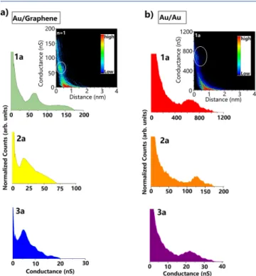
RESULTS AND DISCUSSIONThe conductances of four different series of molecular junctions were measured. For all these molecular junctions studied, 1D and 2D conductance histograms have been plotted. For each 1D conductance histogram, a clear peak dominates. InFigure 2a, we show 1D conductance histograms
of Au/(thiol-terminated PPP)/graphene junctions. Each histo-gram reveals a broad and nonperfect Gaussian distribution peak indicating the most probable conductance values of 68.0 (Au/1a/graphene), 18.5 (Au/2a/graphene), and 5.00 nS (Au/ 3a/graphene). The conductance is clearly highly dependent on the number of phenyl rings in the target compound. In addition, there is a broad peak in the 1D histogram of the Au/ 1a/graphene junction with a full width at half-maximum (FWHM) value of 18.2 nS after Gaussian peak fitting. The corresponding 2D histogram (shown in inset ofFigure 2a) also
reveals a broad distribution of conductance values, as indicated by the white ring.
In order to get a rigorous comparison with standard metallic junctions, we have also measured the thiol-terminated PPP molecules bound to a pair of Au electrodes. The 1D conductance histograms of Au/(thiol-terminated PPP)/Au are shown inFigure 2b, and the inset shows the corresponding 2D histogram of Au/1a/Au junctions. Each of the 1D conductance histograms shows a very broad peak with nonperfect Gaussian distribution. This kind of broad peak is likely to arise from a combination of several individual peaks resulting from the flexible configuration of Au/(thiol-terminated PPP)/Au systems, which agrees well with a previously reported statement of Ulrich et al.28 They found that the Au/(thiol-terminated PPP)/Au system has a high degree of static disorder (each manifestation of the junction is different from the previous one) and dynamic disorder (the junctions can switch spontaneously between different config-urations). We have listed here the most probable conductance values of Au/(thiol-terminated PPP)/Au inTable 1, which are
645 nS for Au/1a/Au, 126 nS for Au/2a/Au, and 23.2 nS for Au/3a/Au. These conductance values correspond to the most likely molecular junction configuration being formed under our experimental conditions. The conductance value of 1a bound between gold electrode pairs has also been widely discussed in previous studies.1,28−31However, on the basis of the diversity in the reported conductance values for 1a, it is clear that there is no a universal consensus. The reported conductance of 1,4-benzenedithiol (BDT) linked with Au electrodes ranges from 31 nS1(4× 10⁻⁴G0, G0= 2e2/h, which is the quantum contact
conductance) to 7740 nS31(0.1G0), and most of these studies
displayed a broad peak in the 1D conductance histogram. Bürkle et al. have reported the conductance of Au/2a/Au junctions.32They found the torsion angle between each phenyl ring could affect the conductance value of the molecular junction. Clearly, it is not straightforward to compare the conductance values for thiol-terminated PPP molecules in Au/ Au configurations reported from different research groups.
We further explored the dependence of the conductance of single molecular junctions on the anchoring group and electrode material by considering also amine-terminated PPP molecules in both Au/Au and Au/graphene configurations. The measured 1D conductance histograms are shown inFigure
Figure 2. (a) Normalized 1D conductance histograms of Au/1a/ graphene, Au/2a/graphene, and Au/3a/graphene (the inset shows the 2D conductance histogram of Au/1a/graphene, where the white ring indicates the distribution of conductance of the molecular junctions). (b) The normalized 1D conductance histograms of Au/1a/Au, Au/ 2a/Au, and Au/3a/Au (the inset shows the 2D conductance histogram of Au/1a/Au, where the white ring indicates the distribution of conductance of the molecular junctions).
Table 1. Conductance Value and Tunneling Decay Value (β) for Four Types of Molecular Junctionsa
conductance (nS) decay constantβ molecular junctions experiment theory experiment theory
Au/1a/graphene 68.0 57.8 Au/2a/graphene 18.5 22.7 1.31 1.10 Au/3a/graphene 5.00 6.40 Au/1b/graphene 58.2 69.2 Au/2b/graphene 13.5 12.0 1.40 1.17 Au/3b/graphene 3.50 6.60 Au/1a/Au 645 Au/2a/Au 126 1.64 Au/3a/Au 23.2 Au/1b/Au 478 Au/2b/Au 82.0 1.38 Au/3b/Au 30.0
aThe decay constant is per phenyl group.
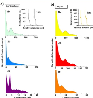
3a (Au/(amine-terminated PPP)/graphene) and Figure 3b (Au/(amine-terminated PPP)/Au). The inset pictures in
Figure 3a,b represent the individual I(s) traces of Au/1b/ graphene (gray) and Au/1b/Au (dark yellow) junctions. These curves highlight the similarities and key differences between the Au electrode and graphene electrode. A clear plateau is seen around 58 nS for the formation of stable Au/1b/graphene junctions. In the case of using gold electrodes, we see a plateau appearing at a much higher conductance close to 500 nS, which is attributed to the formation of Au/1b/Au junctions.
Each 1D conductance histogram reveals the predominant peak corresponding to the most likely junction configuration, and it is clear that the conductance decreases exponentially with the number of phenyl rings in both systems. The measured details are listed in Table 1, and the following conductance values have been recorded: 478 (Au/1b/Au), 82.0 (Au/2b/Au), and 30.0 nS (Au/3b/Au) as well as 58.2 (Au/1b/graphene), 13.5 (Au/2b/graphene), and 3.50 nS (Au/ 3b/graphene), respectively. The corresponding conductance values are obviously much higher for Au/Au systems when compared to Au/graphene systems, which we attribute to contact resistance. In addition, when comparing the Au/(thiol-terminated PPP)/graphene system with the Au/(amine-terminated PPP)/graphene system, it can be seen that the conductance values of the latter are slightly lower.
Similarly, Venkataraman et al. have studied the length dependence of the conductance using the STM-BJ method for a range of amine-terminated molecules, including alkanes33 and oligophenyls.14,24 In Figure 4a, we compare the natural logarithmic conductance plots of our experimental measure-ments with the ones reported by the Venkataraman group. The attenuation trend satisfies the equation G = A exp(−βL),
where β is the decay constant, L is the number of phenyl groups, and A is a constant related to the interaction between the molecular target and the electrode, which reflects the contact resistance. Theβ value is readily calculated from the slope of the plot of ln(G) versus L. For Au/(amine-terminated PPP)/Au junctions, our experimental results (red) are in good agreement with the results presented by the Venkataraman group (green), which indicates that both the STM-BJ and STM I(s) methods are effective for forming these gold-contacted molecular junctions. More importantly, the measure-ments on Au/amine-terminated PPP/graphene junctions yield β = 1.40 per phenyl group, which is essentially the same as Au/ amine-terminated PPP/Au junctions (β = 1.38 per phenyl group). These experimental results show that the decay constant is essentially the same for amine-terminated PPP measured between Au/graphite (Figure 4a, blue, Venkataramn result) and Au/Au (Figure 4a, green) electrodes, which is in good agreement with the results reported in the literature.14,24 Hence, we find that the decay constant β of PPP-based molecular junctions is independent of the electrode material, contrary to alkane-based molecular junctions, where, impor-tantly, the use of a graphene electrode reduces this decay.11,12 Summarizing the experimental results detailed above, the following general observations can be made:
(1) Both amine- and thiol-terminated PPP systems can form junctions with a graphene contact on one side and with gold as the other contact.
(2) Conductance values for the Au/Au systems are much higher than the corresponding Au/graphene systems. (3) Au/(thiol-terminated PPP)/graphene junctions have
slightly higher conductances than the corresponding Au/(amine-terminated PPP)/graphene systems. (4) The conductance attenuation with molecular length (β
value) is broadly similar for Au/Au and Au/graphene systems, irrespective of whether amine or thiol-terminated analogues are used.
Figure 3.(a) Normalized 1D conductance histograms for Au/1b/ graphene, Au/2b/graphene, and Au/3b/graphene molecular junctions (the inset shows two individual I(s) traces for Au/1b/graphene junctions). (b) Normalized 1D conductance histograms for Au/1b/ Au, Au/2b/Au, and Au/3b/Au molecular junctions (the inset shows two individual I(s) traces for Au/1b/Au junctions).
Figure 4. (a) Natural logarithmic plots of the conductance as a function of the number of phenyl rings for amine-terminated PPP, experimentally measured for the Au/Au system (red) and in the Au/ graphene system (yellow). The green line shows literature data for the Au/Au system,24 and the blue line shows literature data for Au/ graphite system.14(b) Natural logarithmic plot of the conductance as a function of the number of phenyl rings. The amine and thiol terminal groups have been compared in the Au/graphene system. The yellow (blue) lines represent the experimental (theoretical) decay values of Au/(amine-terminated PPP)/graphene junctions. The red (green) lines represent the experimental (theoretical) decay values of Au/(thiol-terminated PPP)/graphene junctions.
ACS Applied Nano Materials Article
DOI:10.1021/acsanm.8b01379
ACS Appl. Nano Mater. 2019, 2, 12−18 15
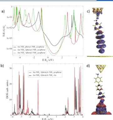
To provide further insight into the experimental results, we have performed DFT calculations to model these molecular junction systems. In Figure4b, we compare the experimental and theoretical attenuation trends of amine-terminated PPP molecular junctions (experimental = yellow, theoretical = blue) and thiol-terminated PPP molecular junctions (experimental = red, theoretical = green) for the Au/graphene system. The present experimental and theoretical results are consistent with each other. Moreover, both experimental and theoretical results produce similar attenuation factors for thiol- and amine-terminated molecular junctions in the Au/graphene case. For example, we note that the experimental measured conductance decay constant β is almost the same for Au/ amine-terminated PPP/graphene (1.40 per phenyl ring, or 0.33 Å−1) and Au/thiol-terminated PPP/graphene (1.31 per phenyl ring, or 0.31 Å−1). This phenomenon is similar to our previous studies where we have obtained a similar decay constant for Au/alkanedithiol/graphene and Au/alkanediamine/graphene junctions.11,12 Table 1 compares the details of experimental and theoretical electrical properties of these four series of molecular junctions. The corresponding calculated trans-missions for Au/(thiol-terminated PPP)/graphene and Au/ (amine-terminated PPP)/graphene are presented inFigures 5a and6a, respectively.
In order to understand the similarities in the attenuation factors between gold−gold and gold−graphene junctions for the PPP-based junctions, we have calculated the density of states (DOS) for the three-phenyl chains in both gold−gold and gold−graphene junction configurations. The results are presented inFigure 5b for the dithiol case and Figure 6b for the diamine case. As is shown, the DOS is very similar for gold−gold or gold−graphene junctions for both types of
anchoring groups, in particular around the energy gap. In the case of amine groups, very small differences in the positions of the molecular levels can be observed, with however very little impact on the electronic transport properties of the junction, in agreement with the experimental data. This peculiar behavior explains why the attenuation factors β remain the same for both types of electrodes, since β mainly depends on the molecular electronic structure. Note that this result is very different from what has been obtained previously with alkane chains,11,12where the introduction of the graphene electrode resulted in a symmetry breaking in the junctions and a drastic reduction of the attenuation factors. Here the introduction of the graphene electrode does not bring the same symmetry breaking despite a weak coupling at the corresponding interface. This feature is further illustrated through calculations and corresponding visualizations of the HOMO isoelectronic DOS for both junctions. These are presented inFigures 5c,d for the dithiol and 6c,d for the diamine. For the different electrode types, namely gold and graphene, and both thiol and amine anchoring groups, the HOMO orbital presents the same out of plane π symmetry, which propagates well along the molecular backbone. Despite the weak coupling at the graphene contact, for both the thiol- and amine-terminated PPP backbones, these anchoring groups couple well and rather similarly with the molecular backbone orbital as seen from the DOS comparison in Figures 5c and 6c. This ensures the electronic propagation along the PPP backbone giving similar attenuation factors for Au/amine-terminated PPP/graphene and Au/thiol-terminated PPP/graphene junctions. This situation is rather different from the more complex situation observed in alkane chains, where the coupling to the molecular chain of thiol or amine was notably different.11
Summarizing the theoretical results detailed above, the following general conclusions can be succinctly made:
Figure 5.(a) Calculated transmissions for the Au/(thiol-terminated PPP)/graphene junctions (n = 1, 2, and 3). (b) DOS comparison for Au/3a/Au and Au/3a/graphene junctions. (c,d) Representations of the Au/3a/graphene and Au/3a/Au junctions, showing the respective HOMO wave functions.
Figure 6.(a) Calculated transmissions for the Au/(amine-terminated PPP)/graphene junctions (n = 1, 2, and 3). (b) DOS comparison for Au/3b/Au and Au/3b/graphene junctions. (c,d) Representation of the Au/3b/graphene and Au/3b/Au junctions, showing the respective HOMO wave functions.
(1) The much higher conductance values for the Au/Au systems than the corresponding Au/graphene systems for both amine- and thiol-terminated PPP wires are a result of the weak coupling at the molecule/graphene interface.
(2) The similarβ values for all junctions studied here are a result of the similar DOS electronic propagation along the PPP backbone; in other words, these values are primarily a function of the PPP molecular backbone and not the anchoring groups or electrode contacts.
■
CONCLUSIONUsing the STM I(s) method, we have determined the electronic conductance and attenuation factor of the current in phenyl-chain-based molecular junctions, with both thiol or amine anchoring groups, using gold−gold or gold−graphene electrodes. In all these cases, we obtain very similar attenuation factors. This contrasts with previous studies with saturated molecular chains (“alkane”), where the introduction of a graphene electrode drastically reduced the attenuation factor. These results are confirmed by DFT calculations, which show very little modification of the electronic DOS using gold−gold or gold−graphene electrodes. This result is explained by the π symmetry of the HOMO orbital, which couples well with all the anchoring groups and electrodes ensuring a propagation along the molecular backbone with consistently the same attenuation factor for amine- or thiol-terminated PPP-based compounds. As a consequence, the decay constantβ for the phenyl chains is dominated by the intrinsic molecular properties and remains almost unaffected by the coupling to the electrode or the anchoring group. On the other hand, the conductance of Au/graphene molecular junctions is much lower than equivalent Au/Au junctions because of the weak coupling at the molecule/graphene interface for both amine and thiol anchors.
■
AUTHOR INFORMATION Corresponding Author *E-mail:[email protected]. ORCID Richard J. Nichols:0000-0002-1446-8275 Li Yang:0000-0002-1040-4223 Author ContributionsShuhui Tao carried out the main experiments and wrote the first draft of the manuscript; Li Yang, Yannick J. Dappe, and Richard J. Nichols wrote the manuscript and designed experiments; Qian Zhang, Chunhui He, and Ruochen Xie conducted other complementary experiments; Cezhou Zhao, Chun Zhao, and Xiangfei Lin analyzed experimental results. Alexander Smogunov and Yannick J. Dappe developed the simulation work and analyzed sequencing simulation data. All authors have given approval to the final version of the manuscript.
Funding
This work was supported by the National Natural Science Foundation of China (NSFC Grants 21750110441, 21503169), the Suzhou Industrial Park Initiative Platform Development for Suzhou Municipal Key Lab for New Energy Technology (RR0140), the Key Program Special Fund in XJTLU (KSF-A-04 and KSF-A-07), and the XJTLU Research Development Fund (PGRS-13-01-03, RDF-14-02-42, and RDF-16-01-33).
Notes
The authors declare no competingfinancial interest.
■
REFERENCES(1) Reed, M. A.; Zhou, C.; Muller, C. J.; Burgin, T. P.; Tour, J. M. Conductance of a molecular junction. Science 1997, 278, 252−254.
(2) Xu, B.; Tao, N. J. Measurement of Single-Molecule Resistance by Repeated Formation of Molecular Junctions. Science 2003, 301, 1221−1223.
(3) Cui, X. D.; Primak, A.; Zarate, X.; Tomfohr, J.; Sankey, O. F.; Moore, A. L.; Moore, T. A.; Gust, D.; Harris, G.; Lindsay, S. M. Reproducible Measurement of Single-Molecule Conductivity. Science 2001, 294, 571−574.
(4) Haiss, W.; van Zalinge, H.; Higgins, S. J.; Bethell, D.; Höbenreich, H.; Schiffrin, D. J.; Nichols, R. J. Redox state dependence of single molecule conductivity. J. Am. Chem. Soc. 2003, 125, 15294− 15295.
(5) Kergueris, C.; Bourgoin, J. P.; Palacin, S.; Esteve, D.; Urbina, C.; Magoga, M.; Joachim, C. Electron transport through a metal-molecule-metal junction. Phys. Rev. B: Condens. Matter Mater. Phys. 1999, 59, 12505−12513.
(6) Kiguchi, M.; Miura, S.; Takahashi, T.; Hara, K.; Sawamura, M.; Murakoshi, K. Conductance of Single 1,4-Benzenediamine Molecule Bridging between Au and Pt Electrodes. J. Phys. Chem. C 2008, 112, 13349−13352.
(7) Yokota, K.; Taniguchi, M.; Kawai, T. Metal−Molecule Interfaces Formed by Noble-Metal−Chalcogen Bonds for Nanoscale Molecular Devices. J. Phys. Chem. C 2010, 114, 4044−4050.
(8) Ahn, S.; Aradhya, S. V.; Klausen, R. S.; Capozzi, B.; Roy, X.; Steigerwald, M. L.; Nuckolls, C.; Venkataraman, L. Electronic transport and mechanical stability of carboxyl linked single-molecule junctions. Phys. Chem. Chem. Phys. 2012, 14, 13841−13845.
(9) Peng, Z. L.; Chen, Z. B.; Zhou, X. Y.; Sun, Y. Y.; Liang, J.-H.; Niu, Z. J.; Zhou, X. S.; Mao, B. W. Single Molecule Conductance of Carboxylic Acids Contacting Ag and Cu Electrodes. J. Phys. Chem. C 2012, 116, 21699−21705.
(10) Guo, X. F.; Small, J. P.; Klare, J. E.; Wang, Y. L.; Purewal, M. S.; Tam, I. W.; Hong, B. H.; Caldwell, R.; Huang, L. M.; O’Brien, S.; et al. Covalently bridging gaps in single-walled carbon nanotubes with conducting molecules. Science 2006, 311, 356−359.
(11) Zhang, Q.; Tao, S.; Yi, R.; He, C.; Zhao, C.; Su, W.; Smogunov, A.; Dappe, Y. J.; Nichols, R. J.; Yang, L. Symmetry Effects on Attenuation Factors in Graphene-Based Molecular Junctions. J. Phys. Chem. Lett. 2017, 8, 5987−5992.
(12) Zhang, Q.; Liu, L.; Tao, S.; Wang, C.; Zhao, C.; Gonzalez, C.; Dappe, Y. J.; Nichols, R. J.; Yang, L. Charge transport through dicarboxylic-acid-terminated alkanes bound to graphene-gold nanogap electrodes. Nano Lett. 2016, 16, 6534−6540.
(13) Liu, L.; Zhang, Q.; Tao, S.; Zhao, C.; Almutib, E.; Al-Galiby, Q.; Bailey, S. W. D.; Grace, L.; Lambert, C. J.; Du, J.; Yang, L. Charge transport through dicarboxylic-acid-terminated alkanes bound to graphene-gold nanogap electrodes. Nanoscale 2016, 8, 14507−14513. (14) Kim, T.; Liu, Z.; Lee, C.; Neaton, J. B.; Venkataraman, L. Charge transport and rectification in molecular junctions formed with carbon-based electrodes. Proc. Natl. Acad. Sci. U. S. A. 2014, 111, 10928−10932.
(15) Vezzoli, A.; Brooke, R. J.; Ferri, N.; Higgins, S. J.; Schwarzacher, W.; Nichols, R. J. Single-Molecule Transport at a Rectifying GaAs Contact. Nano Lett. 2017, 17, 1109−1115.
(16) Vezzoli, A.; Brooke, R. J.; Higgins, S. J.; Schwarzacher, W.; Nichols, R. J. Single-Molecule Photocurrent at a Metal-Molecule-Semiconductor Junction. Nano Lett. 2017, 17, 6702−6707.
(17) Aragones, A. C.; Darwish, N.; Ciampi, S.; Sanz, F.; Gooding, J. J.; Diez-Perez, I. Single-molecule electrical contacts on silicon electrodes under ambient conditions. Nat. Commun. 2017, 8, 15056. (18) Bolotin, K. I.; Sikes, K. J.; Jiang, Z.; Klima, M.; Fudenberg, G.; Hone, J.; Kim, P.; Stormer, H. L. Ultrahigh electron mobility in suspended graphene. Solid State Commun. 2008, 146, 351−355.
ACS Applied Nano Materials Article
DOI:10.1021/acsanm.8b01379
ACS Appl. Nano Mater. 2019, 2, 12−18 17
(19) Lee, C.; Wei, X.; Kysar, J. W.; Hone, J. Measurement of the elastic properties and intrinsic strength of monolayer graphene. Science 2008, 321, 385−388.
(20) Chen, W.; Widawsky, J. R.; Vázquez, H.; Schneebeli, S. T.; Hybertsen, M. S.; Breslow, R.; Venkataraman, L. Highly conducting π-conjugated molecular junctions covalently bonded to gold electro-des. J. Am. Chem. Soc. 2011, 133, 17160−17163.
(21) Xu, B. Q.; Li, X. L.; Xiao, X. Y.; Sakaguchi, H.; Tao, N. J. Electromechanical and Conductance Switching Properties of Single Oligothiophene Molecules. Nano Lett. 2005, 5, 1491−1495.
(22) Tao, N. J. Electron transport in molecular junctions. Nat. Nanotechnol. 2006, 1, 173−181.
(23) Nakazumi, T.; Kaneko, S.; Matsushita, R.; Kiguchi, M. Electric conductance of single ethylene and acetylene molecules bridging between pt electrodes. J. Phys. Chem. C 2012, 116, 18250−18255.
(24) Kim, T.; Vázquez, H.; Hybertsen, M. S.; Venkataraman, L. Conductance of Molecular Junctions Formed with Silver Electrodes. Nano Lett. 2013, 13, 3358−2264.
(25) Hong, W.; Manrique, D. Z.; Moreno-García, P.; Gulcur, M.; Mishchenko, A.; Lambert, C. J.; Bryce, M. R.; Wandlowski, T. Single Molecular Conductance of Tolanes: Experimental and Theoretical Study on the Junction Evolution Dependent on the Anchoring Group. J. Am. Chem. Soc. 2012, 134, 2292−2304.
(26) Mishchenko, A.; Zotti, L. A.; Vonlanthen, D.; Burkle, M.; Pauly, F.; Cuevas, J. C.; Mayor, M.; Wandlowski, T. Single-Molecule Junctions Based on Nitrile-Terminated Biphenyls: A Promising New Anchoring Group. J. Am. Chem. Soc. 2011, 133, 184−187.
(27) Ren, B.; Picardi, G.; Pettinger, B. Preparation of gold tips suisection for tip-enhanced Raman spectroscopy and light emission by electrochemical etching. Rev. Sci. Instrum. 2004, 75, 837−841.
(28) Ulrich, J.; Esrail, D.; Pontius, D.; Venkataraman, L.; Millar, D.; Doerrer, L. H. Variability of Conductance in Molecular Junctions. J. Phys. Chem. B 2006, 110, 2462−2466.
(29) Xiao, X. Y.; Xu, B. Q.; Tao, N. J. Measurement of single molecule conductance: benzenedithiol and benzenedimethanethiol. Nano Lett. 2004, 4, 267−271.
(30) Emberly, E. G.; Kirczenow, G. Theoretical Study of Electrical Conduction Through a Molecule Connected to Metallic Nano-contacts. Phys. Rev. B: Condens. Matter Mater. Phys. 1998, 58, 10911− 10920.
(31) Tsutsui, M.; Teramae, Y.; Kurokawa, S.; Sakai, A. High-conductance states of single benzenedithiol molecules. Appl. Phys. Lett. 2006, 89, 163111−163113.
(32) Bürkle, M.; Viljas, J. K.; Mishchenko, A.; Vonlanthen, D.; Schön, G.; Mayor, M.; Wandlowski, T.; Pauly, F. Conduction mechanisms in biphenyl-dithiol single-molecule junctions. Phys. Rev. B: Condens. Matter Mater. Phys. 2012, 85, 075417.
(33) Venkataraman, L.; Klare, J.; Tam, I.; Nuckolls, C.; Hybertsen, M.; Steigerwald, M. Single-Molecule Circuits with Well-Defined Molecular Conductance. Nano Lett. 2006, 6, 458−462.