HAL Id: hal-00762136
https://hal.archives-ouvertes.fr/hal-00762136
Submitted on 24 Jan 2019HAL is a multi-disciplinary open access archive for the deposit and dissemination of sci-entific research documents, whether they are pub-lished or not. The documents may come from teaching and research institutions in France or abroad, or from public or private research centers.
L’archive ouverte pluridisciplinaire HAL, est destinée au dépôt et à la diffusion de documents scientifiques de niveau recherche, publiés ou non, émanant des établissements d’enseignement et de recherche français ou étrangers, des laboratoires publics ou privés.
Effect of HCl on the doping and shape control of silicon
nanowires
P. Gentile, A. Solanki, N. Pauc, F. Oehler, B. Salem, G. Rosaz, T. Baron, M.
den Hertog, V. Calvo.
To cite this version:
P. Gentile, A. Solanki, N. Pauc, F. Oehler, B. Salem, et al.. Effect of HCl on the doping and shape control of silicon nanowires. Nanotechnology, Institute of Physics, 2012, 23 (21), pp.215702. �hal-00762136�
Effect of HCl on the doping and shape control of Silicon
nanowires.
P. Gentile1, A. Solanki1, N. Pauc1, F. Oehler1*, B. Salem2, G. Rosaz1,2, T. Baron2, M. Den Hertog3V. Calvo1
1
SiNaPS Lab.- SP2M, UMR-E CEA/UJF-Grenoble 1, INAC, Grenoble, F-38054, France
2
LTM/CNRS-CEA-LETI, 17, rue des martyrs, 38054 Grenoble, France
3
CNRS, Institut Néel - Université Joseph Fourier, BP 166, F-38042 Grenoble, France
E-mail:[email protected]
Abstract. The introduction of Hydrogen Chloride during the in-situ doping of Silicon
Nanowires (SiNWs) grown using the Vapour Liquid Solid (VLS) mechanism was investigated. Compared with non-chlorinated atmospheres, the use of HCl with dopant gases considerably improves the surface morphology of the SiNWs, leading to extremely smooth surfaces and a greatly reduced tapering. The variations in the wire diameter are massively reduced for boron doping, and can not be measured at 600°C for phosphorous over several tens of micrometers. This remarkable feature is accompanied by a frozen gold migration from the catalyst, with no noticeable levels of gold clusters observed using scanning electron microscopy. A detailed study of the NWs apparent resistivity reveals that the dopant incorporation is effective for both types of doping. A graph linking the apparent resistivity to the dopant to silane dilution ratio is built for both types of doping and discussed in the frame of the previous results.
1
Introduction
Semiconductor nanowires (NWs) are the topic of intense research in many fields of solid state physics due to their potential use in high performance electronics[1-6], chemical sensors[7,8], solar cells[9-13], and energy storage[14-16]. In the case of silicon nanowires (SiNWs), mass-production is possible using bottom-up methods based on the Vapor-Liquid-Solid process [16, 17] (VLS). Controlled doping of SiNWs obtained by these methods is a prerequisite to any industrial application. Using Chemical Vapor Deposition (CVD), p- and n-type doping of the wires can be performed in-situ, during growth, by introducing the appropriate dopant precursor, B2H6, (p type) or PH3(n type), in addition to the SiH4 gas.
*Now at University of Cambridge, Dpt of Materials Science and Metallurgy, United Kingdom. Pembroke Street,
Cambridge, CB2 3QZ, UK
In-situ doping of NWs is not a recent topic since reports were made as soon as the early 2000s [18] using a gas mixture composed of silane and dopant precursor—see for instance in [19, 20, 23]. However, compared with n type, there is a lack of data regarding the p doping of Si NWs. Different precursors can be used, such as diborane (B2H6) [20, 23] or TriMethylBoron
(TMB) [18, 22]. Resistivity measurements show dispersed values for B2H6 and a rather low
concentration of active impurities for TMB. In addition, as the B2H6 gases are introduced in the
vapour phase, multiple problems can occur, such as morphological changes [24], amorphous shell overgrowth [25, 26]. Some of theses shortcomings can be avoided if the partial pressure of the dopant gases is kept low relative to the Si precursor. A ratio of pB2H6/pSiH4<10
-3
or pPH3/pSiH4<10
-3
permits nanowire growth using Au catalysts in most standard experimental conditions without significant morphological changes. However the problem of shell overgrowth is not solved by these simple pressure adjustments.
Shell overgrowth is concurrent with the main axial growth and originates from a radical change in the radial growth rate induced by the dopant gases. The latter can i) directly change the surface composition by simple vapour-solid reactions and/or ii) increase the gold cluster migration from the main catalyst, also changing the radial growth rate by gold-catalyzed surface growth [27]. P type wires (grown using B2H6) are considerably more affected than n-type wires
(grown using PH3) and p type segments typically show a larger sidewall roughness than their
n-type or undoped counterparts [18, 26].
In our previous works, the role of Hydrogen Chloride (HCl) in the Au-catalyzed SiNWs growth was investigated using a HCl/SiH4gas mixture. The presence of Cl was shown to inhibit
the gold diffusion on Si surfaces [27]—see figure S1—thus stopping colloid diffusion and coalescence at the early stages of the growth sequence and hindering the catalyst loss during the wire axial growth. Together with a decrease of the 2D growth in Cl chemistries, HCl is particularly suitable to fabricate highly straight structures. The chemistry of the surface of undoped SiNWs (gold covered, gold free and/or Cl-passivated) was also proved to be
determinant in the development of the facets or the shell of the wires [28], making use of HCl extremely efficient to keep very smooth surfaces.
In this paper, we examine the effect of the HCl introduction in the growth recipes used for making doped Si NWs. In particular, we show that p and n type doped SiNWs can respectively be obtained using HCl/SiH4/B2H6 and HCl/SiH4/PH3 gas mixtures while retaining the same
surface state—tapering, roughness and presence of gold clusters—as the undoped SiNWs grown using the HCl/SiH4 gas mixture. It is particularly shown that efficient p type doping of Si NWs
can be achieved with the same ease as for the n type one and without an amorphous shell growth.
2
Experimental details
SiNWs are grown in a low-pressure CVD reactor (EasyTube3000 First Nano, a Division of CVD Equipment Corporation) operating at 600 or 650°C and 3 Torr total pressure. We use this temperature range for a good epitaxial growth with high growth rate (500 to 650 nm/mn) compared with lower growth temperature [23]. Si <111> wafers are used as growth substrates and cleaned by dipping in acetone, isopropyl alcohol and deoxidation in HF 10%. If needed, size calibrated SiNWs are grown from gold colloids (BritishBioCell), with a 50 to 200 nm diameter. Alternatively, an evaporated thin gold film ( 3nm) can be used as catalyst. Hydrogen (H2) is used as the carrier gas (1.9 standard liters per minute) while Silane (SiH4) is used as the
Si precursor (20-50 sccm, standard cubic centimetres, or 30 to 80 mTorr for SiH4 partial
pressure). P type and n type doping are respectively achieved by introducing B2H6 and PH3 in
the reactor, with pB2H6/pSiH4 and pPH3/pSiH4 ratios in the 10 -6
to 10-2 range. Depending on the experiment, an additional HCl flux can be introduced in the reactor (0-100 sccm, or 0 to 160 mTorr HCl partial pressure). Scanning electron microscopy (SEM) images were made using a ZEISS ultrascan scanning electron microscope (SEM) equipped with an in lens secondary electron detector. High resolution transmission electron microscopy (HRTEM) images were obtained on a CM300 TEM working at 300 kV.
3
Results and discussion:
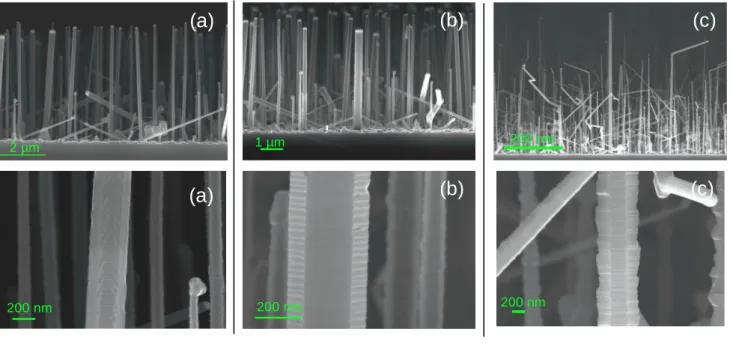
Figure 1 presents p-type SiNWs grown with SiH4 and B2H6(without HCl) on a dewetted gold
thin film at 650°C for different dopant to silane ratios. We observe an increase of the tapering (diameter variation from 5nm/µ m to 15nm/µ m) and the surface roughness with the increase of pB2H6/pSiH4 ratio. Large and rough epitaxial facets are also clearly visible at the largest
pB2H6/pSiH4ratio, as expected from the literature [26].
The rough and irregular wire surface obtained with the standard B2H6/SiH4 gas mixtures is in
stark contrast with the smooth wires previously obtained with the HCl/SiH4 gas mixture [27,
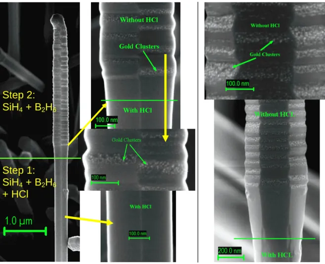
28]. As a reminder, Figure S1 (supplementary information) presents the surface of a wire which was grown alternatively with and without HCl (all other experimental parameters remaining constant). The first segment, grown using HCl, presents a gold free surface with smooth facets and a constant diameter. The second segment, grown without HCl, shows a gold-clustered and irregular surface with large facets and a varying diameter. In light of these results, the use of HCl seems a logical response to the morphological problems encountered in the figure 1 on doped SiNWs. Adding diborane to this reactive gas mixture leads to similar results, as illustrated in figure 2. The conditions of this growth are a temperature of 650°C, a total pressure of 3 Torr, a H2flow of 1L/mn, a SiH4flow of 50 sccm and pB2H6/pSiH4 =1x10
-3
. The first stage is performed with HCl (100 sccm), then the HCl mass flow is closed in the second half of the growth. The SEM images clearly show two distinct regions corresponding to the two growth conditions. The enlarged view of the transition region shows a diameter enlargement and roughness increase as Cl is removed from the reactive mixture, attributed to the increase of the 2D growth, and a white-spotted surface for free HCl conditions. These spots were attributed to gold clusters using a comparative study on undoped Si NWs with SEM imaging and localized EDX analysis in a TEM microscope [29]. On the contrary, the enlarged view of the region grown under an HCl atmosphere shows a smooth surface, with a constant diameter, and no noticeable amounts of gold clusters are observable using SEM imaging. So HCl acts to reduce dramatically the gold migration onto the surface of the wires during the growth of doped Si
NWs, which is in line with our previous work [27, 28]. This limitation of gold migration is due to the chlorination of the NWs surface [28].
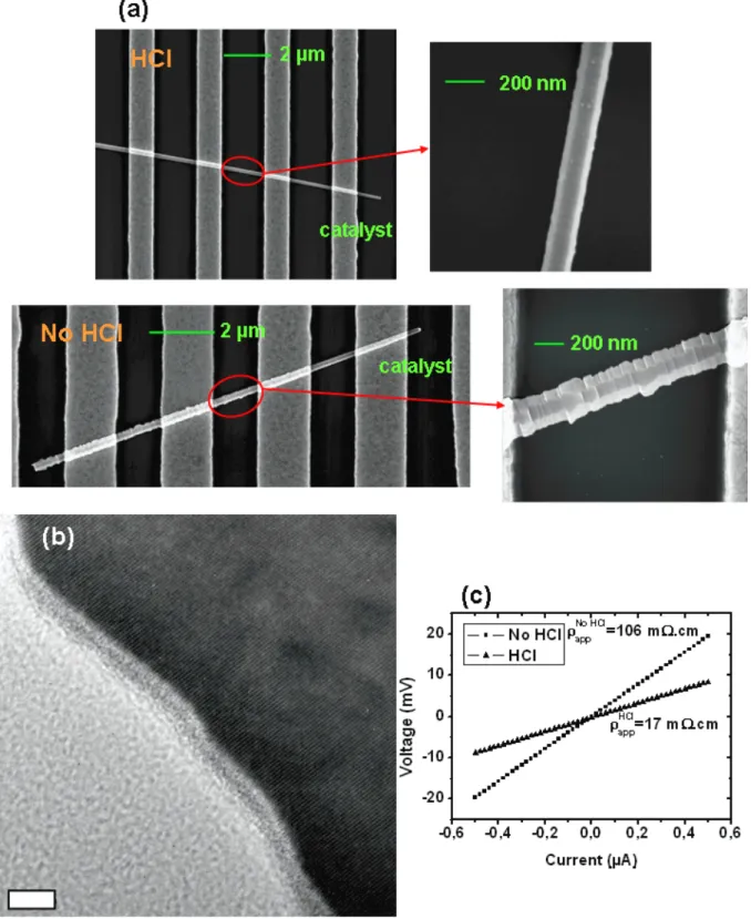
In figure 3, we compare the growth of p-type and n-type SiNWs with and without HCl. The wires were grown at: i) 650°C, 3 Torr and pB2H6/pSiH4 =1x10
-3
(figure 3a and 3b), ii) 600°C and pPH3/pSiH4 =1x10
-3
(figure 3c and 3d), using 100 nm diameter gold colloids. HCl-free recipes lead to very different growth regimes compared with the chlorinated counterparts. Without HCl, the strong catalyst migration (see inset in figure 3c) during growth can induce a total depletion of the catalytic head long before the end of the deposition step. The corresponding wires are much shorter in height and not terminated by a catalyst. The minimum wire diameter for stable growth [27] is here much larger (> 3 x Diam.) than the gold colloids used (100nm) and normal growth only marginally occurs in gold-rich zones (colloid aggregates). In addition, significant tapering (10-30 nm/µ m) and rough surface are clearly observed, a trend which was already observed in the undoped structures grown without HCl and which is attributed to gold-cluster enhanced radial growth and to the reduction of the catalyst size during the growth. The addition of HCl in the B2H6/SiH4 mixture leads to a considerable
increase of the growth yield per colloid—the proportion of colloids which start and gives rise to a complete growth, without growth stop due to catalyst loss—with a great reduction of the wire tapering, nearly not measurable (6nm/µ m at 650°C and 0.25 nm/µ m at 600°C), despite the quite long—20 µ m—length of NWs. These features are in line with the results obtained on undoped wires grown using HCl/SiH4 gas mixtures [26].
Resistivity measurements in a four probes configuration were then performed to assess the electrical properties of the n and p type wires grown with and without HCl. The SiNWs were first sonicated in isopropyl alcohol and drop casted onto oxidized Si samples. Metal contacts were fabricated by optical lithography, metal deposition (Ni-Au for p type wires and Ti-Au for n type wires), and lift off [30]. In a first experiment, SiNWs grown from 200 nm colloids (650°C, 3 Torr, 50 sccm SiH4, pB2H6/pSiH4=10
-3
), with or without HCl were characterized. Due to the strong tapering usually found in the free HCl atmospheres, which considerably widens the
base diameter, it was impossible to connect these regions owing to the limited thickness of the photoresist. Thus, regions close to the foot of these NWs could not be connected using a lift off process, which further restricted the I(V) analyses to the regions close to the top of the NWs.
To achieve a meaningful comparison between the two samples, great care was given to the choice of region probed. Indeed, axial dependant resistivity measurements performed on the same NW revealed an increasing resistivity for decreasing catalyst to probed section distance. This trend was already observed in phosphorous doped Si NWs grown without HCl and attributed to very efficient dopant diffusion from the surface to the core of the NW for temperatures as small as 460°C [31] thus contributing to the so-called surface doping. Here axial dependant changes in the resistivity were observed both for n and p type dopings, with, for instance, a resistivity drop from 10 to 6 m .cm all across a 20 µ m length boron doped wire grown at 650°C under HCl and pB2H6:pSiH4=10
-3
. The figure 4 (a) shows two connected wires (p type, with and without HCl) and the corresponding probed regions, both approximately situated 4 microns from the catalyst. This ensures that the electrical measurements originate from wire segments which share a comparable surface exposure to the doping gases during the growth. This latter point is justified by experimental verification of equal growth rates in both chemistries.
As expected, tapering is more pronounced for HCl free growth conditions, with an experimental diameter enlargement of 11.0 nm/µ m compared to 6.3 nm/µ m with HCl. In the figure 4 (a), the enlarged views of the electrically probed sections confirm the stark morphological contrast between the two chemistries. The experimental apparent resistivities are
app= 106 mΩ.cm without HCl (mean diameter of 223 nm) and app= 17 mΩ.cm with HCl (mean
diameter of 155 nm). Assuming that the hole mobility in the wires does not deviate too much from the bulk material—i. e. in the range of 100 cm2/V.s for the impurity concentrations under study—we can extract the density of ionized impurities in the wires and obtain NA(223 nm, no
HCl) = 2x1017 cm-3 and NA (155 nm, HCl) = 4x10 18
cm-3 respectively. Such a discrepancy between the two samples is not well understood but could be explained by several factors, like a
bad estimate of the effective cross section for the carrier transport in the rough nanowire due to the strong faceting. High gold concentrations and surface roughness in the HCl free nanowire could lower the hole mobility, or a very high density of surface states might contribute to trap the free carriers and increase the apparent resistivity of the HCl free wires.
A HRTEM image obtained on an as grown wire coming from the same sample than the one presented in 4 (a) is shown in figure 4 (b) —growth conditions with a HCl atmosphere, a temperature of 650°C and pB2H6/pSiH4=10
-3
. One can clearly see that an amorphous layer of around 2 nm is present on the sidewalls, which is routinely observed on undoped Si NWs and attributed to amorphous native oxide [29]. This feature largely differs from previous TEM analyses carried out on boron doped Si NWs grown at 500°C and using diborane as a precursor, where a thick and amorphous shell was observed under high pB2H6/pSiH4 ratio [26]. This
overgrowth was ascribed to radial growth and exhibits a high density of gold precipitates. In the case of HCl enhanced growth of doped Si wires, uncatalyzed 2D growth and gold diffusion from the catalyst are massively reduced, which in turn stops the formation of any Si shell and preserves the wire crystallinity, while allowing doping in both (n and p) configurations.
In the figure 5 we present the apparent resistivity as a function of the dopant gas to silane ratio for the n and p doped SiNWs. These results are obtained on wires typically 20-30 µ m in length, 100-200 nm in diameter, and display the mean value for the apparent resistivity, when measured at several places across the wire. The values show a decrease of the resistivity as the dopant gas to silane ratio increases, as observed in the literature for wires grown without HCl [21, 26]. The smallest mean apparent resistivity measured from HCl wires was found to be 6 mΩ.cm for p type wires, corresponding to NA 10
19
cm-3—based on use of the bulk mobility— with pB2H6/pSiH4 =10
-3
at 650°C— with low-high values of 1.1 and 12 mΩ.cm for this particular point. The corresponding value for n type wires was measured at 0.6 mΩ.cm (ND 10
20
cm-3) and obtained at 600°C with pPH3/pSiH4= 8x10 -3
. This latter value is in line with the data obtained in ref [21], which reported a resistivity saturation of phosphorous doped SiNWs in a HCl-free configuration around 0.6 mΩ.cm using a similar dopant to silane ratio
(pB2H6/pSiH4= 1.5 10 -2
). Regarding p type doping, the resistivity saturates at 10 m .cm for diborane partial pressures above pB2H6/pSiH4 = 10
-3
in line with the extrapolated value in ref [20] and much lower than the value obtained with TMB [22]. This suggests that a similar saturation mechanism exist for boron impurities at dopant densities close to 1 1019cm-3.
4
Conclusion
In this article, we demonstrate the effect of the combined use of silane and hydrogen chloride in the growth of p and n doped SiNWs. Using this particular reactive mixture, a significant improvement in the wire morphology is obtained compared with the HCl-free approach, with smoother wires surfaces, reduced tapering and permits to keep a good crystallinity without amorphous shell. Limitation of gold diffusion from the catalyst, already observed on undoped SiNWs grown with HCl, is maintained with both PH3 and B2H6 doping gases, thereby making
this process a valuable solution for limiting the gold contamination in doped SiNWs. Resistivity measurements confirm that dopant impurities effectively incorporate in the structure with typical values spanning the m .cm to .cm range for both types of doping. This range fulfils most of the technological requirements in terms of doping level.
Acknowledgments
This work was done with the help of the Nanoscience foundation trough the NEP-IV project.
Keywords:
Chemical vapour deposition • nanowires • Silicon • doping
References
[1] Quitoriano, N. J.; Kamins, T. I. Nano Lett. 2008, 8, 4410–4414.
[2] Cui, Y.; Zhong, Z.; Wang, D.; Wang, W.; Lieber, C. Nano Lett. 2003, 3, 149–152.
[3] Zhong, Z.; Wang, D.; Cui, Y.; Bockrath, M. W.; Lieber, C. M. Science 2003, 302, 1377– 1379.
[4] Goldberger, J.; Hochbaum, A.; Fan, R.; Yang, P. Nano Lett. 2006, 6, 973–977.
[5] V. Schmidt, H. Riel, S. Senz, S. Karg, W. Riess, and U. Gösele, Small 2006, 2(1) 85–88,. 11
[6] G. Rosaz, B. Salem, N. Pauc, P. Gentile, A. Potié, and T. Baron, Microelec. Eng. 2011,
88, 3312-3315
[7] Li, Z.; Chen, Y.; Li, X.; Kamins, T. I.; Nauka, K.; Williams, R. S., Nano Lett. 2004, 4, 245–247.
[8] Cui, Y.; Wei, Q.; Park, H.; Lieber C., Science 2001, 293, 1289–1292
[9] Tian, B.; Zheng, X.; Kempa, T.; Fang, Y.; Yu, N.; Yu, G.; Huang J., Lieber C., Nature 2007, 449, 885–889.
[10] Tsakalakos, L.; Balch, J.; Fronheiser, J.; Korevaar, B.; Sulima, O., Rand J., Appl. Phys. Lett. 2007, 91, 233117.
[11] Erik C. Garnett and Peidong Yang. Silicon, Journal of the American Chemical Society 2008, 130(29), 9224–9225
[12] B.M. Kayes, H.A. Atwater, and N.S. Lewis, Journal of Applied Physics 2005, 97, 114302 [13] B.M. Kayes, M.A. Filler, M.C. Putnam, M.D. Kelzenberg, N.S. Lewis, and H.A. Atwater,
Applied Physics Letters 2007, 91, 103110
[14] C.K. Chan, H. Peng, G. Liu, K. McIlwrath, X.F. Zhang, R.A. Huggins, and Y. Cui, Nature 2008, 3, 31–35
[15] Taeseup Song, Jianliang Xia, Jin-Hyon Lee, Dong Hyun Lee, Moon-Seok Kwon, Jae-Man Choi, Jian Wu, Seok Kwang Doo, Hyuk Chang, Won Il Park, Dong Sik Zang, Hansu Kim, Yonggang Huang, Keh-Chih Hwang, John A. Rogers, and Ungyu Paik, Nano Letters 2010,
10, 1710–1716,
[16] R.S. Wagner and W.C. Ellis, Physics Letters 1964, 4, 89
[17] RS Wagner, WC Ellis, KA Jackson, and SM Arnold, Journal of Applied Physics 1964,
35(10), 2993
[18] Y. Cui, X. Duan, J. Hu, C. M. Lieber, J. Phys. Chem. B 2000, 104, 5213.
[19] V. Schmidt, J. V. Wittemann, S. Senz, and U. Gösele, Adv. Mater. 2009, 21, 2681–2702 [20] M. T. Björk,_ J. Knoch, H. Schmid, H. Riel, and W. Riess, Appl. Phys. Lett 2008, 92,
193504
[21] Heinz Schmid, Mikael T. Björk, J. Knoch, S. Karg, H. Riel, and W. Riess, Nano Lett. 2009, 9, 173-177
[22] Yanfeng Wang, Kok-Keong Lew, Tsung-Ta Ho, Ling Pan, Steven W. Novak, Elizabeth C. Dickey, Joan M. Redwing and Theresa S. Mayer, Nano Lett. 2005, 5, 2139
[23] Lincoln J. Lauhon, Mark S. Gudiksen, Deli Wang and Charles M. Lieber Nature 2002,
420, 57
[24] F. Li, Peter D. Nellist and David J. H. Cockayne, Appl. Phys. Lett. 2009, 94, 263111 [25] Kok-Keong Lew, Ling Pan, Timothy E. Bogart, Sarah M. Dilts, Elizabeth C. Dickey, Joan M.
Redwing, Yanfeng Wang, Marco Cabassi, Theresa S. Mayer, and Steven W. Novak Appl. Phys.
Lett. 2004, 85, 3101
[26] Ling Pan, Kok-Keong Lew, Joan M. Redwing, Elizabeth C. Dickey, J. Cryst. Growth 2005, 277, 428
[27] F Oehler, P Gentile, T Baron and P Ferret, Nanotechnology 2009, 20, 475307
[28] F. Oehler, P. Gentile, T. Baron, P. Ferret, M. Den Hertog, and J. Rouvière, Nano Lett. 2010, 10, 2335–2341
[29] M. I. den Hertog, C. Cayron, P. Gentile, F. Dhalluin, F. Oehler, T.Baron and J.L. Rouviere, Nanotechnology 23 (2012) 025701
[30] G. Rosaz, B. Salem, N. Pauc, P. Gentile, A. Potié, T. Baron, Semicond. Sci. Technol. 2011, 26 085020
Figure 1 SEM images of p-doped SiNWs growth with different pB2H6/pSiH4ratio, at 650°C, 1.5 Torr
total pressure and H2flow of 1.9 L.mn-1, without HCl. The faceting increases with the B/Si ratio due to
2D growth. The tapering increases with pB2H6/pSiH4 ratio: diameter enlargement from 5nm/µm
(pB2H6/pSiH4=2.4x10-5) to 15nm/µm (pB2H6/pSiH4=1x10-3)
B
2H
6/ SiH
4= 2.4x 10
-5B
2H
6/ SiH
4= 1.6x 10
-4B
2H
6/ SiH
4= 1x 10
-3 2 µm(a)
1 µm(b)
200 nm(c)
200 nm(a)
200 nm(b)
200 nm(c)
Figure 2: SEM images of boron doped SiNWs grown in two steps condition: step 1 with HCl and step
2 without HCl. We clearly observe two regions on the NWs corresponding to the two growth conditions. In the zooms showing the region grown without HCl we can clearly observe gold clusters at the surface with an increase of the diameter and the roughness.
Step 1:
SiH
4+ B
2H
6+ HCl
Step 2:
Figure 3: SEM images of p doped (a,b) and n doped (c,d) SiNWs, grown from gold colloids (100 nm
diameter) with dopant to silane ratio equal to 10-3 in both cases, at 650°C for the boron doping and 600°C for the phosphorous doping, without HCl (a, c) and with HCl (b, d). Diameter variations are: i) boron 8-15nm/µm without HCl and 6nm/µm with HCl at 650°C, ii) phosphorous 13nm/µm without HCl and <0.25nm/µm with HCl.
(a)
(b)
Without HCl
With HCl
Boron
Phosphorous
(c)
(d)
Figure 4: (a) Typical SEM views of boron doped Si NWs (pB2H6/pSiH4 =10 -3
) grown with and without HCl (b) TEM enlarged view of a “HCl” wire coming from the same sample than in (a), scale bar is 5 nm, and (c) corresponding current-voltage curves obtained in similar regions.
Figure 5: Mean apparent resistivity of Si NWs grown with HCl for phosphorous doping at 600°C and boron doping at 650°C. 10-5 10-4 10-3 10-2 10-1 100 101 102 103 104 105 R e s is ti v it y (m Ω .c m ) pPH3 B2H6/pSiH4 B 2H6+ HCl, 650°C PH3+ HCl, 600°C