HAL Id: tel-00515370
https://tel.archives-ouvertes.fr/tel-00515370
Submitted on 6 Sep 2010
HAL is a multi-disciplinary open access
archive for the deposit and dissemination of sci-entific research documents, whether they are pub-lished or not. The documents may come from teaching and research institutions in France or abroad, or from public or private research centers.
L’archive ouverte pluridisciplinaire HAL, est destinée au dépôt et à la diffusion de documents scientifiques de niveau recherche, publiés ou non, émanant des établissements d’enseignement et de recherche français ou étrangers, des laboratoires publics ou privés.
microelectronics
Khaled Kaja
To cite this version:
Khaled Kaja. Development of nano-probe techniques for work function assessment and application to materials for microelectronics. Physics [physics]. Université Joseph-Fourier - Grenoble I, 2010. English. �tel-00515370�
D´
eveloppement de techniques nano-sondes
pour la mesure du travail de sortie et
application aux mat´
eriaux en
micro´
electronique
T H E S E
Prepar´
ee au CEA - LETI - MINATEC
Pr´
esent´
ee `
a l’Universit´
e de Grenoble
pour obtenir le grade de
Docteur de l’Universit´
e de Grenoble
sp´
ecialit´
e: nano-physique
par
Khaled KAJA
soutenue le 18 Juin 2010 devant le jury compos´e par :
Pr´esident : Ren´e-Louis Inglebert - Polytech (Grenoble) Rapporteurs : Thierry Melin - CNRS - IEMN (Lille)
Nick Barrett - CEA - IRAMIS (Saclay) Directeur de th`ese : Guy Feuillet - CEA - LETI (Grenoble) Examinateurs: Brice Gautier - INL - INSA (Lyon)
Development of nano-probe techniques
for work function assessment and
application to materials for
microelectronics
PhD T H E S I S
Prepared at CEA - LETI - MINATEC
Defended at the University of Grenoble
to obtain the grade of
Doctor of the University of Grenoble
speciality: nano-physique
by
Khaled KAJA
on 18 June 2010 in front of the jury:
President : Ren´e-Louis Inglebert - Polytech (Grenoble) Reviewers : Thierry Melin - CNRS - IEMN (Lille)
Nick Barrett - CEA - IRAMIS (Saclay) Thesis adviser : Guy Feuillet - CEA - LETI (Grenoble) Examiners: Brice Gautier - INL - INSA (Lyon)
Acknowledgments
First, I want to thank my thesis advisor, Guy Feuillet for the freedom he gave me to explore my ideas. I thank him for his interest in my work and his availability when I needed his help.
I am also very grateful to my two supervisors, Nicolas Chevalier and Olivier Renault, for the interest they had in my work and for their investment. I thank them especially for the time they spent with me in the last part of my doctoral writing. It was a pleasure working with them. I learned a lot thanks to our very interesting discussions. I sincerely hope that we could have the opportunity to work together in the future.
I also thank Fran¸cois Bertin and Amal Chabli for their sincere support and guidance during difficult times I had to go through. I owe them a lot.
I would also like to thank Denis Mariolle for teaching me how to use the KFM. Thanks for all the discussions we had together. I hope we could cooperate in the future.
Many thanks to Aude Bailly and Maylis Lavayssi`ere who were very patient with me while teaching me how to use the NanoESCA. I am deeply grateful to Maylis for the time she had spent to help me getting my XPEEM results and processing all data.
I would also like to express my appreciation and thanks to Philippe Brincard and Fr´ed´eric Laugier for welcoming me aboard when I started my PhD. I also thank Fr´ed´eric and Jean-Claude Royer for their help and support during the last period of my work.
I want to thank all my laboratory colleagues for the pleasant atmosphere they provided each day, especially during coffee (and cake) breaks. Thanks for Cl´ement Gaumer (PBSDM) with whom I shared the office during the entire PhD period. Thanks to Louis Gorintin and all my wishes for the best in his work. Thanks to Christophe Licitra for all the guitar tricks. Thanks to N´evine Rochat for being there to give me good advice when I needed it. Thanks to all my friends in Grenoble for all restaurants, games and activities that we had together. I also thank all my friends AITAP for all the good times spent together.
I deeply thank Pauline for being by my side at the end of my thesis. Without her support and presence, things would have been very difficult.
I want to thank Wiss, Houss, Bach, Abboud and Ssamir just for being the best part of my life. And Taha and Nada, the brother and the sister with whom
I grew up and I found my self a part of their new small family (with Douano!).
Finally, I want to thank my family, my brother and my sister for their support and true love. And last but not least, I present my gratefulness and my admiration for my mother and my father who supported me throughout my life. The words could not express how much I owe them. I am what I am now because they believed in me and gave me all their love and care.
Abstract
The reliable and spatially resolved work function measurement of materials and nanostructures is one of the most important problems in surface characteri-zation for advanced technological applications. Among different methods for work function measurement, AFM-based Kelvin Force Microscopy (KFM) and X-ray Photo-Emission Electron spectro-Microscopy (XPEEM) are two of the most promising techniques.
In this thesis, we were interested in the investigation of local work func-tion measurements using KFM under ambient condifunc-tions, and in the study of complementarities between measurements obtained by KFM and XPEEM. We first present an analysis of KFM measurement variations with the tip-sample distance on various metal samples. These variations can be explained by a simple model based on surface charge transfers associated with the non-homogeneity in local work function. The influence of the tip, environmental and experimental parameters on KFM measurements was also investigated.
We then show an increase in spatial resolution of KFM imaging in air through the implementation on the commercial microscope of an AFM-KFM combined mode, based on the simultaneous acquisition of KFM measurement with that of the surface topography.
Finally, we focus on the characterization of epitaxial graphene layers on SiC(0001) substrate, using both KFM and XPEEM techniques. KFM work function images in air reveal, qualitatively, the heterogeneity of these layers on the sample surface with high spatial resolution. Complementary measurements by XPEEM at the photoemission threshold show that this heterogeneity is related to the increase in work function due to a local variation of graphene layer thickness between 1 and 4-5 monolayers, as reported in literature. This is qualitatively correlated with local intensities from the corresponding Si2p and C1s XPEEM core-level images. Ways for understanding this atypical variation in work function of graphene layers are outlined according to the literature and to micro-spectroscopy results, in terms of electronic coupling with the SiC substrate.
R´
esum´
e
La mesure fiable et spatialement r´esolue du travail de sortie de mat´eriaux et nanostructures est l’un des probl`emes les plus importants en caract´erisation de surface avanc´ee pour les applications technologiques. Parmi les m´ethodes de mesure du travail de sortie disponibles, la microscopie `a sonde de Kelvin (KFM), bas´e sur l’AFM, et la spectromicroscopie de photo´emission d’´electrons par rayons X (XPEEM) apparaissent comme les m´ethodes les plus prometteuses.
Nous nous sommes int´eress´es dans cette th`ese `a l’investigation de la mesure lo-cale du travail de sortie par KFM sous air ainsi qu’`a l’´etude de la compl´ementarit´e entre les mesures obtenues par KFM et XPEEM. Nous pr´esentons tout d’abord une analyse des variations des mesures KFM avec la distance pointe-´echantillon sur diff´erents ´echantillons m´etalliques. Ces variations peuvent ˆetre expliqu´ees par un mod`ele simple bas´e sur des transferts de charges de surfaces associ´es `
a l’inhomog´en´eit´e locale du travail de sortie. L’influence de la pointe, de l’environnement et des param`etres exp´erimentaux a ´et´e aussi ´etudi´e.
Nous avons ensuite mis en ´evidence une augmentation de la r´esolution spatiale de l’imagerie KFM sous air grˆace `a la mise en oeuvre, sur le microscope commercial, d’un mode combin´e AFM-KFM bas´e sur l’acquisition simultan´ee des mesures KFM et de la topographie de surface.
Enfin, nous nous sommes focalis´es sur la caract´erisation crois´ee par KFM et XPEEM de couches de graph`ene ´epitaxi´ees sur un substrat SiC(0001). Les images du travail de sortie obtenues par KFM sous air permettent de r´ev´eler qualitativement, avec une grande r´esolution spatiale, l’h´et´erog´eneit´e de ces couches en surface. La mesure compl´ementaire par XPEEM spectroscopique au seuil de photo´emission montre que cette h´et´erog´eneit´e est li´ee `a l’augmentation du travail de sortie local dˆu `a une ´epaisseur de graph`ene variant entre 1 et 4-5 monocouches d’apr`es la litt´erature. Ceci est corr´el´e qualitativement avec les intensit´es locales Si2p et C1s extraites des images XPEEM correspondantes. Des voies pour la compr´ehension de cette ´evolution atypique du travail de sortie d’un mat´eriau, sont esquiss´ees d’apr`es la litt´erature disponible et les r´esultats micro-spectroscopiques, en terme de couplage ´electronique avec le substrat SiC.
1 Introduction 1
2 Local work function: concepts and experimental methods 5
2.1 What is the ”work function”? . . . 5
2.1.1 Energetic contributions to the work function . . . 7
2.2 The local work function . . . 10
2.2.1 Variations of the surface dipole layer . . . 10
2.2.2 The local vacuum level . . . 12
2.2.3 Changes of local work function induced by adsorbates . . 12
2.2.4 Work function anisotropy . . . 12
2.3 Work function of semiconductors . . . 14
2.4 Work function measurement: principles and experimental techniques 15 2.4.1 Experimental techniques . . . 16
2.5 Fundamental characterization requirements . . . 21
2.5.1 KFM and XPEEM techniques for ultimate work function characterization . . . 21
3 Spatially resolved work function mapping: principles and meth-ods 27 3.1 Kelvin Force Microscopy (KFM) . . . 27
3.1.1 Atomic Force Microscopy: a brief introduction . . . 28
3.1.2 The double scan KFM technique: lift mode . . . 37
3.2 X-ray photo electron emission spectromicroscopy (XPEEM) . . . 48
3.2.1 Introduction . . . 48
3.2.2 XPEEM spectromicroscopy: N anoESCA . . . 54
3.2.3 N anoESCA: description of the instrument . . . 63
3.2.4 Practical aspects of XPEEM experiments: sample handling 66 3.3 Lift mode KFM and XPEEM (N anoESCA): assessment and comparison . . . 69
3.3.1 Advantages and constraints . . . 69
3.3.2 Conclusion: further improvements . . . 69
4 Analysis of experimental effects in KFM measurements 71 4.1 Effects of experimental parameters on the CPD measurements in lift mode . . . 72
4.1.1 Experimental protocol . . . 72
4.1.2 Effect of the tip-sample separation: the lift Height . . . . 73
4.1.3 Effect of the tip shape damages . . . 79
4.1.4 Effect of the environment: relative humidity . . . 80
4.2 Improving the spatial resolution: a single scan method with
multi-frequency excitation at higher eigenmodes . . . 85
4.2.1 Introduction . . . 85
4.2.2 Presentation of our method . . . 88
4.2.3 Application: comparing single scan MF-EFM and KFM lift mode . . . 91
4.2.4 Stability of the method: effects of of the external electrical excitation signal . . . 99
4.2.5 Conclusion and further improvements . . . 103
4.3 Calibration of KFM tips: defining reference sample using KFM and XPEEM . . . 103
4.3.1 The goal of this study . . . 104
4.3.2 Using XPEEM to measure a standard work function value 104 4.3.3 Evolution of the CPD measurements with KFM: Ru as a standard sample . . . 105
4.3.4 Defining a daily KFM calibration routine . . . 109
4.4 General conclusion . . . 109
5 Characterization of epitaxial graphene on SiC (0001) using XPEEM and KFM experiments 111 5.1 Introduction . . . 111
5.1.1 What is graphene? . . . 111
5.1.2 Graphene layers: thickness measurements . . . 114
5.1.3 The sample: epitaxial FLG on SiC(0001) . . . 116
5.2 Methodology of experiments . . . 120
5.3 Experimental Results . . . 120
5.3.1 Raman spectroscopy and µ-Raman imaging . . . 120
5.3.2 µ-XPS: chemical analysis over the entire FoV . . . 122
5.3.3 Work function from threshold XPEEM measurements . . 132
5.3.4 Evidence of topographic changes from KFM measurements 147 5.3.5 Measuring the layer thickness with local spectromicroscopy experiments . . . 158
5.4 General conclusion . . . 174
6 Conclusions 177 A The general expression of the electrostatic energy in EFM 185 A.1 Electrostatic energy of an arbitrary system . . . 185
A.2 Application to KFM experiments . . . 187
B Corrections of instrumentally induced artifacts 189 B.1 The correction of the Schottky effect . . . 189
B.2 The narrowing of the field of view . . . 190
C An overview of existing methods for the characterization of FLG
thickness 195
C.1 Auger Electron Spectroscopy (AES) . . . 195
C.2 Surface X-ray Diffraction (SXRD) . . . 195
C.3 X-ray Photo Emission Spectroscopy (XPS) . . . 196
C.4 Ellipsometry . . . 196
C.5 Low Energy Electron Microscopy (LEEM) . . . 196
C.6 Micro-Raman spectroscopy . . . 197
C.7 Angle Resolved Ultra-violet Spectroscopy (ARUPS) . . . 197
C.8 Low Energy Electron Diffraction (LEED) . . . 198
C.9 Scanning Tunneling Microscopy (STM) . . . 199
C.10 Atomic Force Microscopy (AFM) . . . 199
C.11 Kelvin Force Microscopy (KFM) . . . 200
C.12 X-ray Photo Electron Emission Microscopy (XPEEM) . . . 200
D Practical aspects for XPEEM and KFM coupled experiments 203 D.1 Sample orientation and referential elements . . . 203
D.2 Protocol steps . . . 203
Introduction
T
he work function, which is the minimum energy required to extract an electron from a crystal, is one of the most fundamental properties of materials’ surfaces. It is extremely sensitive to very subtle changes in structure, composition and contamination or any alteration of surface properties of a physical or chemical nature. Therefore, the work function is an important property in many scientific disciplines. It governs the band alignment in semiconductors and forms a fundamental property in the quality of metal-semiconductor contacts, in the determination of residual contamination and the development of new carbon-based devices such as carbon-nanotubes gas nano-sensors or graphene-based transistors.Nowadays developments in nanoscience and nanotechnology create a growing demand for characterization tools to determine the work function on a nanometer scale. The complexity of the systems studied often requires the use of several spectroscopic or structural surface analysis methods. The extreme sensitivity of the work function to the surface quality imposes the need to control the environmental conditions in which measurements are performed. This also requires a good understanding of the environmental effects on the quality of work function measurements. Furthermore, the smaller size of modern technology devices requires measurements with a high spatial resolution to characterize complex heterogeneities in new materials used in micro- and nano- electronics.
Therefore two principal requirements challenge the quality of the intended work function measurements: reliability and high spatial resolution. These nano-characterization requirements call for suitable tools and appropriate experimental protocols whose study and development form the basic core of this thesis.
Among the numerous characterization methods and techniques for determining the materials work functions, Kelvin Force Microscopy (KFM) and X-ray Photo Electron Emission Microscopy (XPEEM) emerge as two of the most powerful and promising tools for reliable and highly resolved work function measurements.
The main goal of our study is to investigate the characterization of the local work function using these two techniques. The objective of this investigation is threefold:
The evaluation of the work function measurement with both techniques in terms of understandings, limitations, differences and quality.
The improvement of KFM measurement capabilities in air for better relia-bility and spatial resolution.
The complementarity between both methods in terms of coupled measure-ments and experimental protocols.
Therefore, this manuscript will be organized as follows:
In chapter 2, we define the work function of metals and semiconductors. We emphasize the property of the local work function and work function anisotropy. Finally we briefly review the experimental methods employed for work function measurements with a particular focus on the spatially resolved techniques used in our study.
In chapter 3, we describe in details the physical and working principles of KFM and XPEEM techniques. We discuss the nature of related image contrasts. We also provide a complete description of each equipment employed as well as the practical aspects of related experiments. We finally draw a first comparative panel between both techniques and point out their complementarity.
In chapter 4, we address the subject of analysis and improvement of KFM measurements in air. We first present a thorough study of the effects of experimental conditions and parameters on conventional KFM measurements. We then present a development of a new operational mode for the improvement of the spatial resolution of measurements.
In chapter 5, we present a complete study coupling both KFM and XPEEM techniques for the investigation of epitaxial few layer graphene grown on SiC(0001) substrate. Our main goal of this study is to characterize the thickness of graphene layers using two-dimensional work function maps obtained with KFM and XPEEM experiments.
L
e travail sortie, d´extraire un electron du volume d’un mat´efini comme ´etant l’´energie minimale n´eriau, est l’une des propriet´ecessaire poures les plus fondamentales des surfaces de mat´eriaux. Grace `a son extreme sensibilit´e `a toute modification subtile des propri´et´es physiques ou chimiques de la surface, le travail de sortie intervient d’une mani`ere fondamentale dans de nombreuses applications physiques.Dans le cas des transistors MOS par exemple, les travaux de sortie du m´etal de grille ainsi que celui du semiconducteur utilis´e dans ces composnants controlent la tension seuil de d´eclenchement et affectent d’une fa¸con directe le fonctionnement des transistors. Dans les cellules photovoltaiques, le travail de sortie de l’´electrode de contacte sup´erieur est directement li´ee `a l’optimisation de la tension du circuit ouvert qui d´etermine l’efficacit´e de conversion en ´energie de ces cellules. Le travail de sortie intervient aussi dans l’alignement des bandes dans les semiconducteurs et les contactes m´etal-semiconducteur. Il constitue une propri´et´e importante pour le d´eveloppement des nouveaux composants micro´electroniques `a base de carbone comme les nano-d´etecteurs de gaz `a base de nanotube de carbone ou les transistors `a base de graph`ene.
Avec les d´eveloppements actuelles des nanosciences et nanotechnologies, la mesure du travail de sortie `a l’´echelle nanom´etrique est devenue l’un des probl`emes les plus importants en caract´erisation de surface avanc´ee pour les applications technologiques. La compl´exit´e des syst`emes ´etudi´es n´ecessite assez souvent l’utilisation de diff´erentes m´ethodes spectroscopiques ou structurales pour la caract´erisation et l’analyse des surfaces.
En plus, la sensibilit´e du travail de sortie `a l’extreme surface ainsi que la r´eduction des dimensions composants utilis´es dans les technologies modernes exigent d’une part le controle des conditions environmentales de la mesure et d’une autre part une r´esolution spatiale ´elev´ee pour la caract´erisation des h´eterogeneit´es complexes dans les nouveaux mat´eriaux utilis´es en micro- et nano-technologies.
Ceci d´efinit les besoins fondamentaux de la nano-caract´erisation du travail de sortie : la fiabilit´e de la mesure et la haute r´esolution spatiale. Ces besoins font appels `a des techniques de caract´erisations adapt´ees et des protocoles de mesures appropri´es dont l’´etude et le d´eveloppement consistuent le coeur de cette th`ese.
Parmi les diff´erentes m´ethodes disponibles pour la d´etermination du travail de sortie, la microscopie `a sonde de Kelvin (ou Kelvin Force Microscopy (KFM)) et la spectromicroscopie de photo´emission d’´electrons par rayons X (XPEEM) apparaissent comme les m´ethodes les plus prometteuses pour une mesure fiable et spatialement r´esolue. L’objectif de cette th`ese concerne l’investigation de la caract´erisation du travail de sortie local en utilisant ces deux m´ethodes. Trois aspects sont ainsi d´evelopp´es :
L’´evaluation des limites et des diff´erences de la mesure du travail de sortie par la technique KFM et la technique XPEEM.
L’am´elioration de la mesure sous air du travail de sortie par KFM pour l’augmentation de la r´esolution spatiale.
L’´etude la compl´ementarit´e entre les deux m´ethodes de mesure KFM et XPEEM.
Local work function: concepts
and experimental methods
D
ans ce chapitre, nous adressons le sujet de la mesure du travailde sortie local. Nous introduisons, dans un premier temps, le con-cept du travail de sortie. Nous consid´erons ensuite les d´efinitions du travail de sortie local et de l’anisotropie du travail de sortie. Finale-ment, nous passons en revue les diff´erentes m´ethodes disponibles pour la d´etermination du travail de sortie en introduisant particuli`erement les deux techniques utilis´ees dans cette th`ese : la microscopie `a force de Kelvin (KFM) et la spectromicroscopie de photo´emission d’´electrons par rayons X (XPEEM).I
N this chapter1 we shall address the leading theme of this thesis: the local work function measurements. We introduce the concept of the work function. We consider properties such as the local work function and the work function anisotropy. An overview of the commonly used methods to measure the work function is presented. In particular, we introduce two techniques used in our studies for the local work function measurements: Kelvin Force Microscopy (KFM) and X-ray Photo Electron Emission Microscopy (XPEEM).2.1
What is the ”work function”?
The work function corresponds to the minimum energy required to extract one electron from a metal. More precisely, the work function is the energy difference between two states of the whole crystal. In the initial state, the neutral crystal containing N electron is assumed to be in its ground state with energy EN. In the final state, one electron is removed outside the crystal, where it is assumed to be at rest and without interaction with its image.
1Historical photos were taken from different web sources, most notably from the Nobel prize
Accordingly, it has only electrostatic potential en-ergy described by the vacuum level, EV. The crys-tal with the remaining N − 1 electrons is assumed to be in its ground state with energy EN −1. This defini-tion calls for zero temperature and a perfect vacuum since the crystal is in its ground state, both before and after electron removal. The work function was first defined in this way by Wigner and Bardeen in 1935 [1].
Therefore, for zero temperature, the work function is given by:
φ = (EN −1+ EV) − EN· (2.1)
For temperatures greater than zero, the removal of an electron from the metal is to be considered as a thermodynamic change of state. The difference EN − EN −1 has to be replaced by the derivative of the Helmholtz free energy F with respect to the electron number N , whereby the temperature T and the volume V are kept constant. This derivative is the chemical potential, µ, of the electrons:
(EN − EN −1) → (∂F/∂N )T ,V = µ, (2.2)
Then, the general expression of the work function2 for non-zero temperature can be written as:
φ = EV − µ· (2.3)
For metals, the chemical potential (µ) remains equal to the Fermi level (EF) to a high degree of precision. In fact the deviation of µ from EF is of the order of T2, which is typically only about 0.01 percent even at room temperature [2]. Therefore, the work function for metals can be written as:
φ = EV − µ = EV − EF· (2.4)
In the definition of the work function, EV represents the electrostatic potential energy of the removed electron at rest, in a region outside the crystal where it is has no interaction with its image. For an infinitely-extended homogeneous crystal, EV is considered at an infinite distance from the crystal surface.
However for a finite non-homogeneous crystal, EV is not considered at infinity because, in general, the work function is different for different crystallographic faces of the crystal. In this case, the distance between the removed electron and a crystal face should be sufficiently large such that the image force can be neglected (typically 10−4 cm) [3]. But, at the same time, this distance should be small compared to that between the electron and any other crystal face with
2
a different work function. Otherwise it is not possible to discriminate between work functions of different crystal faces [4].
2.1.1 Energetic contributions to the work function
In the expression of the work function (equation 2.3) the absolute values of EV and µ depend on the reference energy. If we consider the total average of the bulk electrostatic potential, Ein, as a reference energy level (Ein =0), the work function can be subdivided into two parts (see figure 2.1) [4]:
a surface-dependent part: Ws = EV - Ein
the chemical potential referred to Ein: ¯µ = µ - Ein, which depends on bulk properties only.
The work function3 is therefore given by:
φ = Ws− ¯µ. (2.5)
Equation 2.5 shows the energetic contributions to the work function for a clean surface. However in the presence of surface adsorbate (adatoms or molecules that could be induced by physisorption or chemisorption), another surface contribution, ± |ψ|, is added in equation 2.5 which induces changes in the work function (see section 2.1.1.2). Therefore we can generalize the expression of the work function by showing all energetic contributions:
φ = Ws− ¯µ ± |ψ| · (2.6)
Figure 2.1 (b) shows an energy diagram explaining the different contributions to the work function of metals. It also shows the electrostatic potential energy V near the metal surface. Note that the in presence of adsorbates, their contribution (here considered as + |ψ| in figure 2.1) displaces the position of the vacuum level (see section 2.1.1.2) and changes the electrostatic potential, V , near the surface (dashed line in figure 2.1 (b)).
In the following text we will make use of the terms: ideal surfaces and real surfaces. We consider an ideal surface as infinitely-extended, homogeneous (single crystal) and rigorously flat. A real surface is considered as of finite-size, non-homogeneous (polycrystal) and mostly containing structural or chemical defects.
3It is important to note that the expression in eq.2.5 properly includes all many-body effects,
2.1.1.1 The surface dipole layer
For an clean ideal surface, the surface-dependent contribution Ws (equation 2.5) arises from the presence of a surface dipole layer. This dipole layer is due to the fact that a surface does not present an infinite potential barrier to the electrons within a solid. Although the electrons are bound in the solid, the electronic wave-functions themselves may have a non-zero amplitude ’just outside’ (for prac-tical purposes within 10 ˚A) of the surface [6], which gives rise to ’electron overspill’.
Figure 2.1: (a) the charge density n±(z) distribution perpendicular to a ’Jellium’ surface and
creation of the surface double layer. (b) the potential energy diagram explaining the components of the work function φ of metals. Ws is the surface dipole barrier. ¯µ the chemical potential
referred to Ein, the total average of the bulk electrostatic potential. |ψ| the barrier induced by
surface adsorbates. V the electrostatic potential near the metal surface ad Vimthe potential of
the image interaction [7].
As shown in figure 2.1 (a) for the Jellium-model4, the distribution of positive charges n+(z) (z, normal to the surface) abruptly falls to zero at the surface. However, the negative charge distribution n−(z) leaks beyond the geometrical surface plane (z = 0) thereby creating an excess of negative charge in front of the surface [7] [1].
To preserve overall electrical neutrality, the excess negative charge in front of the surface is balanced by a corresponding excess positive charge at the solid surface. Hence the surface dipole layer is formed.
Therefore this dipole layer induces an energy step Ws that the electron must overcome to leave the metal [7]. The moment of dipoles in this layer tends to confine electrons in the conduction band of the crystal and therefore increases the work function. A higher density of surface dipoles leads thus to a higher work function [8]. The value of Ws is determined by the manner 4In the Jellium model, the positive ions in the metal are replaced by a uniform positive
background which exert an attractive electrostatic interaction on all the electrons of the system. The mathematical analysis of this model allows for the determination of the electronic density inside the metal and at the surface as well [5].
in which the charge distribution in the surface cells differs from that of the bulk [2].
The effect of Ws on the work function value has been pointed out by Smoluchowski in 1941 [8]. Smoluchowski determined the electron density for different crystallographic planes of the same crystal. He showed that the work function of a loosely packed crystal face is smaller than that of a closely packed face for face-centered cubic structure (fcc) metals. The density of surface dipoles is related to the atomic packing in the surface plane. Therefore, Ws increases with the packing density of a crystal plane, which explains the variation of the work function. This has been experimentally observed by XPEEM and KFM experiments for the different faces of Cu [9] [10].
This phenomenon introduces the concept of work function anisotropy for real surfaces, which will be discussed in section 2.2.4.
2.1.1.2 Work function changes induced by adsorbates
In ambient environment, samples are exposed to gaseous atoms and molecules which may adsorb on the surface. Adsorbates can either be induced by chemisorption or physisorption (see figure 2.2).
Figure 2.2: Surface dipole induced by the chemisorption of (a) electropositive adsorbates and (b) electronegative adsorbate on the metal surface. The transfer of charge between the adsorbate and the substrate, or vice versa, results in the formation of surface dipoles. (c) simple model of physisorbed atom consisting of a positive ion and a valence electron. The attractive interaction with the solid is due to screening (image charges) [3] [6].
In the case of chemisorption, a charge transfer occurs between the adsorbate and surface. Electropositive adsorbates (figure 2.2 (a)) tend to transfer electron charge from their outer valence shell to the substrate. As a result of this transfer, a net positive charge now resides on the adsorbate inducing an equal but opposite
image charge at an equivalent distance below the surface plane [6]. This results in the formation of a dipole moment, where the distance between the positive and negative charges is d, as illustrated on figure 2.2 (a). Electronegative adsorbates usually possess an unfilled affinity level and the charge transfer occurs in the opposite sense, i.e. from substrate to adsorbate (figure 2.2 (b)).
In physisorption of an atom for example, the valence electron and the nucleus of the adsorbed atom interact with their images below the surface plane (see figure 2.2 (c)). A resulting dipole moment is formed which depends on the distance z between atom and surface. For more details see [3].
The dipole moment induced by adsorbates gives rise to an additional electric field that acts on the electron leaving the surface. The direction of this field depends on the nature of the adsorbate as described above. This creates an energy barrier, ± |ψ|, that is added to the one resulting from the surface dipole layer. The position of the vacuum level is therefore shifted (see figure 2.1(b)).
The presence of adsorbates on the surface induces changes in the work function as described in equation 2.5. The sign of this change depends on the nature of adsorbates (− |ψ| for electropositive adsorbates and + |ψ| for electronegative ones). Work function changes by adsorbates are used in monitoring the atomic coverage of species on metal surfaces (for example, alkali atoms on the surface of a single crystal Ni) [11].
2.2
The local work function
The local work function is an important property of real surfaces. It depends on the local quality of the surface which may vary due to the presence of local defects (structural or chemical), atomic steps or edges [7]. It may also vary with the local properties of the surface such as the presence of different crystallographic orientations [9] [10], locally embedded charges [12] or local changes in the doping level [13] in case of a semi-conducting surface (see section 2.3).
Here we discuss the local work function and we identify effects resulting from its variation over the surface, i.e. the work function anisotropy (see below).
2.2.1 Variations of the surface dipole layer
As previously discussed in section 2.1.1 the work function has two basic components: the electrochemical potential (¯µ) and the barrier from the surface dipole layer (Ws) (see equation 2.5). While ¯µ depends on bulk properties only [4], Ws is sensitively dependent on the surface conditions.
The value of Ws depends on the density of surface dipoles resulting from the electron ”overspill” outside the surface. The density of dipoles itself is dependent on the atomistic structure at the surface. For a real (non-homogeneous) surface, lateral changes in the atomistic structure (caused by one of the reasons mentioned above) are therefore equivalent to a lateral modulation of the surface dipole density. Accordingly, Ws will vary paral-lel to the surface and its value will depend on its specific location ,i.e. Ws(i)(xi, yi).
Figure 2.3: An example of a real surface of metal showing three facets with different crys-tallographic orientations (represented as hatched zones for illustration). The energy diagrams showing the components ¯µ and Ws for each facet.
Perhaps the case of a clean polycrystalline surface is the best example to illustrate this fact. We consider in figure 2.3 a clean (with no adsorbates) metal surface with three facets of different crystallographic orientations. We represent energy diagrams showing the energetic components of the work function for each facet.
At thermodynamic equilibrium the chemical potential, ¯µ, and the total average electrostatic potential, Ein, inside the bulk are constant. Then, the change of the atomic structure (here related to the crystallographic orientation) is reflected in the variation of Ws(i) for each facet. Therefore the local work function of a specific facet (located at (xi, yi) on the surface) is given by:
φlocal= φ(i)(xi, yi) = Ws(i)(xi, yi) − ¯µ· (2.7) For a clean polycrystalline surface of Cu, KFM and XPEEM experiments have determined the local work function of grains with different orientations [9] [10]. Results showed that φ111 > φ100> φ110, in agreement with theoretical predictions by Smoluchowski [8] for fcc metals.
Note that the example used for illustration can be generalized, i.e. a real metal surface could present inequivalent facets due to any of the reasons mentioned in the introduction of this section (structural defects, chemical defects or changes in the local geometry of the surface for example).
2.2.2 The local vacuum level
Local variations of Ws(i) at the surface of the same metal are equivalent to local variations of the vacuum energy level, EV(i) (see figure 2.3). Hence EV(i) acquires the character of local vacuum level [14].
Therefore, the variation in the local work function at different locations (xi, yi) and (xj, yj) on the surface with different local properties corresponds to:
φ(i)− φ(j)= EV(i)− EV(j)· (2.8)
The local vacuum level, EV(i), describes the energy in the final state of the electron removed from a specific location on the metal surface. Therefore, EV(i) is defined in a region ”just outside” the surface, i.e. a region where the electron in the final state is no longer in interaction with its image charge.
Accordingly, the local work function (φlocal) corresponds to the minimum energy required to extract an electron from the highest occupied state in the metal (EF = µ) to the local vacuum level (EV(i)) outside the surface.
2.2.3 Changes of local work function induced by adsorbates
The effect induced by adsorbates on an ideal surface’s work function has been detailed in section 2.1.1.2. Here, for the case of a real (non-homogeneous) surface, the effect is the same. Therefore, if we consider adsorbates homogeneously distributed on the surface of the metal, the local work function could be written as:
φ(i)= Ws(i)− ¯µ ± |ψ| (2.9)
where the ± depends on the nature of the adsorbate (see section 2.1.1.2) .
2.2.4 Work function anisotropy
The work function anisotropy is the variation of the local work function at different regions on the surface of a crystal. Inequivalent regions on the surface with different work functions are called ”patches” [15] [16]. ”Patches” may be due to surface preparation, to the uneven distribution of
adsorbates, to crystallographic orientations or to variations in surface local geometry [16]. Surfaces used in all technological applications may present
many of these aspects. Therefore it is interesting to address the work func-tion anisotropy and show its effect on the measurement of the local work funcfunc-tion.
In presence of inequivalent patches on the surface, macroscopic surface charges may develop on patches (in addition to the surface dipole layer), provided that the total charge of the whole crystal surface remains zero [2] [16] [17]. These macroscopic charges are called ”patch charges”.
Figure 2.4: Zero total work is done in taking an electron from an inte-rior level at the Fermi energy over the path shown, returning it at the end to an interior level at the Fermi energy. That work, however, is the sum of three contributions: φA/e (in
going from 1 to 2), 1/e(φA− φB)
(in going from 2 to 3, where φA/e
and φB/e are the electrostatic
po-tentials just outside faces A and B), and −φB/e (in going from 3 back to
1) [2].
Consider a crystal with two inequivalent faces (patches) A and B, as illus-trated in figure 2.4. The work function of the two faces are different, i.e. φA6= φB.
If one takes an electron (initially at EF) out of the crystal through face A, the energy spent to do so is the work function φA= WsA− ¯µ. Now bringing it back in again to EF through face B, the energy spent is: −φB = ¯µ − WsB.
The total work done in such a cycle mush vanish, if energy is to be conserved. However, this is not actually the case here. The total energy spent in extracting the electron from A and reintroducing it back through B is:
Etotal = WsA− WsB= φA− φB, (2.10)
which is not conserved since φA6= φB.
There must therefore be an electric field outside the metal against which a compensating amount of work is done as the electron is carried from face A to face B. In other words, the two faces must be at two different electrostatic potentials VA and VB such that:
Since the surface dipole layer cannot yield macroscopic fields outside of the metal, the electric field outside the metal must arise from net macroscopic distributions of electric charges5 on the surface (known as ”patch charges”) [2] [16]. Therefore the surface charge density must change from region to region. Note that the condition for the whole crystal to be neutral requires that the sum of the macroscopic surface charges over all regions (entire surface) must vanish [2].
This phenomenon is known as the ”patch charge” effect [17]. It has long been known that patch charges affect electron trajectories in field emission microscopy [17] [18]. Electric fields induced by patch charges outside polycrystalline surfaces have been detected experimentally close to the surface by force microscopy techniques [17]. As we shall see later (see chapter 4), patch charge effect can explain variations observed in Kelvin force microscopy measurements [19].
2.3
Work function of semiconductors
Semiconductors are characterized by a band gap, Eg, between the valence band and the conduction band. In a non-degenerated semiconductor, the position of the Fermi level, EF, is in the band gap. For an intrinsic semiconductor (no doping), EF is close to the middle of the band gap at T = 0 K. For a doped semiconductor, the position of EF within the band gap depends on the nature of doping.
For an N -type silicon semiconductor (for example, using phosphor atoms for doping), the position of EF is closer to the minimum of the conduction band, ECB (see figure 2.5). For a P -type silicon semiconductor (for example, using bore atoms for doping), EF is closer to the maximum of the valence band, EV B. For the definition of the work function of a semiconductor we first introduce two properties: the electron affinity, χ, and the ionization energy, IE.
χ at a semiconductor surface is defined as the energy required to excite an electron from the bottom of the conduction band (ECB) at the surface to the local vacuum level (figure 2.5). Similarly, the ionization energy IE is defined as the energy needed to excite an electron from the top of the valence band (EV B) at the surface to the local vacuum level [14].
Figure 2.5 shows an energy band diagram of a N -type semiconductor near its surface. eVBB results from the band bending at the surface of the semiconductor. Regarding all these energies, the work function can therefore be defined by one
5
Patch charge densities, compared to charge densities in the surface dipole layer, are very small. Patch charge densities are in the range of 10−9 electrons/˚A2, while the estimated order
Figure 2.5: Energy band of a semi-conductor near its surface showing the band bending eVBB, the electron
affin-ity χ, the ionization energy IE, the band gap Eg and the edges of the
con-duction and valence band, ECB and
EV Brespectively [14].
of the following expressions:
φs= χ + eVBB+ (ECB − EF)bulk
φs= IE + eVBB+ (EF − EV B)bulk (2.12)
Semiconductor’s work function is relevant in all contact applications and Schottky barrier measurements which are widely employed for the characterization of the materials’ resistivity and dopant profiling. Interested readers can find details about these subjects elsewhere [13] [3] [20] [21] [22].
2.4
Work function measurement: principles and
ex-perimental techniques
As discussed in section 2.2.4, real surfaces present a work function anisotropy resulting from the presence of surface patches. Experimental techniques should therefore measure the local work function of each patch on the surface, otherwise the work function anisotropy is lost. To do so, the final state in which the electron emitted from the surface is detected should correspond to the local vacuum level (see section 2.2.2).
In fact, this would not be possible if the detector was simply placed very far from the surface. Because in that case, the final state of the detected electron would be described by the vacuum level at infinity. It follows that for an anisotropic surface, a single work function will be measured as only an average. Its value is intermediate between the maximum and minimum work functions of the different patches on the surface.
Experimentally, detectors used to measure the work function are usually far from the sample surface. However to measure the local work function and characterize the surface anisotropy, external electric fields are applied in order to collect the electrons emitted from the surface.
If each electron reaching the detector can be associated with a particular emitting patch by observing its trajectory, then the work function of each patch can be inferred from its associated electron current. The electron current emitted from each patch is determined by the potential shape, and particularly by the maximum potential that the electrons must overcome. Even for small electric fields, this maximum is located close to the crystal surface and thus depends on the local work function of the patch [23].
In this way, the lateral work function anisotropy can be observed and the local work function is measured. The spatial resolution of measurements is determined by technical limitations of the experimental tool used to measure the work function.
2.4.1 Experimental techniques
The techniques for determining the work functions can be broadly classified into two groups. The first class of experiments aims at measuring the work function on an absolute scale and is based on electron emission processes. By stimulating a metallic surface in various ways, a current of electrons is produced, from which the work function is determined. The stimulus can consist of photons (photoelectric effect and UPS), be of a thermal nature (thermionic emission),
con-sist of an applied electric field field emission or be a combination of these methods.
The second class of techniques concentrates on obtaining work function differences, either between various metals (Kelvin probe) or during surface modifications, such as adsorption processes. Work function measurements with these methods are relative and usually require a determination of a standard reference work function. Experimental protocols, combining techniques from both classes are often elaborated for reliable work function measurements.
In the following paragraphs, we shall briefly describe the common techniques available for work function determination. Technical details can be found in standard textbooks, to which interested readers are referred [15] [24] [3].
2.4.1.1 Electron emission-based techniques Photoelectric measurements
When radiation, of frequency ν, is incident on a metal surface, photoelectrons are produced, provided that hν ≥ φ (φ is the metal work function). The threshold
frequency, ν0, at which electrons start leaving the metal is defined by hν0 = φ. Theoretical analysis, originally conducted by Fowler in 1931, shows that the quantum yield I (photoelectrons per light quantum absorbed) is related to ν - in the region which is not too close to the threshold frequency - by the equation:
I = bh2(ν − ν0)2/2k2, (2.13)
where b is a material-dependent value related to the probability of absorbing a photon. k is the Boltzman constant and h the Planck constant. If I1/2 is plotted against ν, then the extrapolation to zero would determine ν0 and hence the work function φ. This zero-temperature approximation is the procedure commonly used to interpret experimental results. Corrections may be included to account for the collecting electric field, which lowers the surface barrier slightly [15].
The Ultraviolet Photoelectron Spectroscopy (UPS)
In UPS, a monochromatic ultraviolet light source of known frequency ν (Hg, D2 or He discharging lamps) is used to illuminate the surface of a sample.
Electrons in the valence band (of energy Ei with respect to the vacuum) are then excited into states above the vacuum level and may be emitted from the crystal if the hν ≥ φ condition is satisfied. Emitted electrons are detected and counted by sweeping their kinetic energies.
The recorded spectrum consists of primary electrons as well as secondary electrons of lower kinetic energy. The secondary electrons result from inelastic scattering of the primary electrons during the emission process, and have kinetic energies down to zero. The total width of the spectrum of the emitted electrons is equal to hν − φ, thus providing a measure of the work function φ.
The thermionic emission
When heating a metallic surface to high temperature T , in the range of 1000-1500 K, a fraction of the electrons acquire sufficient energy to leave the metal. Using thermodynamic theory, one can show that the saturation electron current density J can be approximated by the Richardson-Dushman formula [25]:
J (T ) = A(1 − r)T2exp(−φ/kBT ) (2.14)
where A = emk2B/2π2~3 is a universal constant and r is the mean reflection probability for electrons incident on the metal surface in the equilibrium state. The determination of φ from measurements of the current J , as a function of the temperature T , is complicated by various factors. A collecting field E is applied to measure J , which lowers the work function slightly and induces a supplementary parameter which needs to be extrapolated to zero. The temperature dependence of work functions is usually around ±10−3 - 10−4 eV/K [23].
2.4.1.2 Work function differences-based techniques Contact potential difference: the Kelvin probe
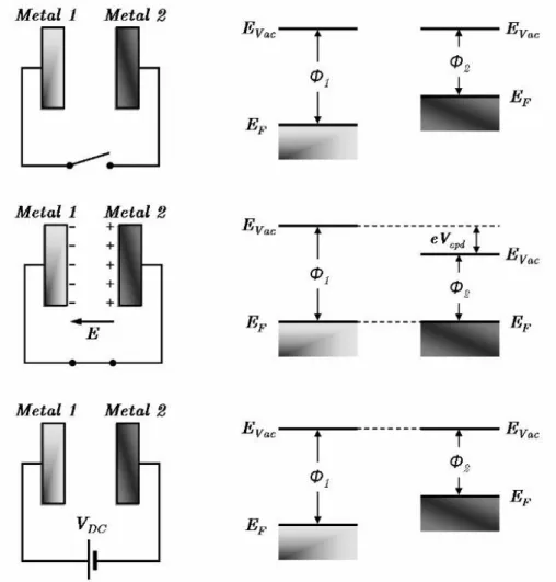
The Contact Potential Difference (CPD) method provides a measure of a sample’s work function relative to that of a reference metal [26]. It was first proposed by William Thomson (Lord Kelvin) in 1898, hence known as the Kelvin Probe (KP) technique. The KP technique relies on the existence of a potential difference outside the surface of two different metals electrically connected.
When metals are connected, the electrons start flowing from the metal with lower work function to the one with higher work function, until the electrochemical potential in both connected metals is the same, hence Fermi levels aligning (criterion of thermodynamic equilibrium). This movement of charges induces the appearance of a potential difference between the two metals, called the contact potential difference, Vcpd, which is equal to the initial work function difference existing before contact between the probe (φ1) and the sample (φ2) (see figure 2.6).
The establishment of the Vcpd can be easily observed by measuring the electric field ~E induced between the two metallic electrodes. In order to measure contact potential difference, this electric field can be then canceled out by the application of an external bias voltage VDC between electrodes. Once ~E is null, then VDC = Vcpd. Consequently, the work function of the sample electrode can be obtained by:
φ2 = φ1− |e| VDC (2.15)
provided that the work function of the probe (φ1), also known as the reference electrode, is identified6.
The vibrating capacitor: Zissman method
In 1932, W.A. Zissman proposed an improved version of the Kelvin probe technique, in which the reference electrode (the probe), of several mm2, was set to vibrate above a fixed sample electrode. Hence, a vibrating capacitor is formed when both electrodes are connected, where the distance between them varies as d0+ A cos(ωt). d0 is the initial mean distance between electrodes before vibration, and A and ω are respectively the amplitude and the frequency of the reference electrode vibration.
The physical principle is the same as in the Kelvin probe method (see figure 2.6). However, the vibration of the present capacitor will induce an alternative
6
Figure 2.7: A simplified scheme of the Zissman method of the vibrating capacitor. The current i(t) flowing between the probe and sample elec-trodes is nullified by adjusting VDC
which is therefore equal to Vcpd.
current i(t) to flow between electrodes due to the movement of the capacitive charges on the capacitor plates (see figure 2.7):
i(t) = dC
dt V ≈ C0 A d0
ω sin(ωt) (VDC− Vcpd) · (2.16)
Hence, in Zissman’s method, the Vcpd value is obtained by nullifying the current i(t) which provides VDC = Vcpd. The work function of the sample is then determined according to the expression 2.15. The accuracy of this method can reach ∼1 meV; however, the spatial resolution is limited by the size of the probe electrode (i.e. ∼ µm). The obtained work function consists of an averaged value where the local information about its variation is lost.
The diode methods
An alternative method for measuring work function differences and variations was suggested by Anderson in 1935 [27]. Here, a slow beam of electrons is thermally emitted from a cathode source and is accelerated by an electric field onto the sample of interest that constitutes the anode. The beam size is large on the atomic scale but small compared with the crystal surface.
The resulting current I is measured as a function of the potential difference V applied between the electrodes. If the work function of the sample changes, the I − V characteristic of the diode shifts horizontally. Usually a feedback mechanism fixes the current, which allows the work function change to be directly revealed from the difference in the applied potential. If the beam is produced by
an electron gun and slowed down near the sample, it can be scanned across the substrate, allowing work function maps to be produced [28]. This technique has been widely applied for in situ studies of gas adsorption on metallic surfaces [23].
2.4.1.3 Experimental data
Work function compilations for a large number of metals with various crystallo-graphic orientations have been published in [29] [30] [31] [32] [33]. Some selected values are shown in table 2.1. Values were obtained using different techniques discussed in the previous paragraphs.
2.5
Fundamental characterization requirements
There are three major implications concerning measurement’s quality and char-acterization tools for work function determination in view of modern technology.
High spatial resolution forms a major necessity for the characterization of work function changes at the deca-nanometer scale, imposed by the drastic scaling of devices in new-technology applications.
Reliable and absolute measurements are of crucial importance in most applications. Because the work function is extremely sensitive to the surface quality, contamination and environmental effects can lead to significant alterations. The need for appropriate characterization tools and experimental protocols is therefore of great importance.
In-line characterization The ability to characterize the work function at different stages during device fabrication is also a fundamental necessity in the field of micro- and nano- electronic applications. This point is not discussed in this work.
In this thesis, we used two complementary characterization techniques for work function measurements: Kelvin Force Microscopy (KFM) and X-ray Photo Electron Emission Microscopy (XPEEM).
2.5.1 KFM and XPEEM techniques for ultimate work function characterization
Kelvin Force Microscopy (KFM)
Also known as Kelvin Probe Force Microscopy (KPFM). This is an ultimate extension of the Kelvin probe method.
Element W.F.(eV) Technique Reference Au 4.25 Th. [34] 5.1 P.E. [30] 5.4 P.E. [35] 5.45 C.P.D. [36] 5.22 C.P.D. [37] 5.4 C.P.D. [35] Al 4.36 P.E. [38] 4.08 P.E. [39] 4.2 P.E. [40] 4.24 C.P.D. [41] 4.19 C.P.D. [42] 4.18 C.P.D. [37] Cu 4.5 Th. (1160 - 1280 K) [34] 4.6 Th. (∼1350 K) [43] 4.4 Th. (1100 - 1300 K) [44] 4.6 C.P.D. [41] 4.51 C.P.D. [42] 4.8 (111) P.E. [9] 4.5 (100) P.E. [9] 4.4 (110) P.E. [9] 4.55 (poly) P.E. [9] Pt 5.3 - 5.5 Th. (1600 - 1900 K) [45] 5.08 Th. [31] 5.65 P.E. [29] 5.2 P.E. [46] 4.52 C.P.D. [31] 5.36 C.P.D. [31] 4.82 C.P.D. [47] Ru 4.71 P.E. [30] 4.52 C.P.D. [48] W 4.52 Th. (1350 - 2200 K) [49] 4.5 Th. (1820 - 2940 K) [50] 4.6 P.E. [51] 4.49 P.E. [52] 4.55 C.P.D. [42] 4.38 C.P.D. [43]
Table 2.1: Experimental work function values, in eV, of selected metals (acquired from [33]). Values were obtained using different techniques, Th.: Thermoionic emission, P.E.: Photo Electric threshold, C.P.D.: Contact Potential Difference.
After the invention of the Atomic Force Microscopy (AFM) in 1986 by Binning et al., the idea of adapting the Zissman’s method to AFM was proposed in 1991 by Nonnenmacher et al. [53]. A conducting AFM tip and surface form a vibrating capacitor in which the very small dimension of the AFM tip plays a crucial role in improving the spatial resolution of the contact potential difference measurements. Differing from Zissman’s method, the measurement of Vcpd with KFM is based on the detection and nullification of an electrical force arising between the two electrodes of the tip/sample capacitor instead of measuring a current7.
Almost similar to Zissman’s method, the feedback principle of KFM is based on adjusting an external bias voltage VDC until the electrical force vanishes and hence VDC = Vcpd, where:
Vcpd=
φtip− φsample
|e| (2.17)
allows to determine the value of φsampleprovided that φtip is identified8. In KFM measurements, the tip scans the sample surface and thus allows one to obtain two-dimensional maps of the Vcpd lateral variations. Moreover, it offers the interesting possibility of simultaneously measuring the variation of topography which provides important complementary information for most applications.
KFM provides high spatial resolution measurements due to the dimensions of the AFM tips (tip apex ∼ 10 nm). KFM can operate in ambient conditions and UHV environments. Its accuracy can reach 10 mV in air and is ten times higher under UHV thanks to the improved quality factor of the tip’s oscillations (see chapter 3). Its working principle and installation make it a powerful candidate as an in-line characterization tool to monitor device fabrication process.
Figure 2.8 shows an example of typical KFM images (topography (a) and contact potential difference (b)) obtained under ambient conditions for a clean polycrystalline copper surface. The work function map of copper with the crystallographic grain orientations was recorded with a spatial resolution ∼ 50 nm.
However, the KFM technique suffers from the relative character of its contact potential difference measurements. Calibration protocols are therefore needed to allow quantitative or semi-quantitative results.
X-ray Photo Electron Emission Microscopy (XPEEM)
7Indeed, due to the small value of the capacitance, the current is too small to be measured 8
Figure 2.8: (a) Topography of a clean copper surface showing the boundaries of grains, (b) the work function map extracted from the Vcpdimage obtained simultaneously in KFM experiments.
The variation of the work function of copper with the grain orientations is emphasized and work function maps are recorded with a spatial resolution of ∼ 50 nm [10].
The photoelectron emission microscopy (PEEM) was invented by Br¨uche in the early 1930s [54]. Since then the improvement of PEEM benefited from several breakthroughs in related fields, such as the improvement in the quality of ultra-high vacuum (UHV), the invention and development of a variety of surface sensitive methods for structural and chemical analysis (in particular photoemission spectroscopy).
PEEM principle is based on the collection of the electrons emitted from a sam-ple surface after irradiation with photons [55]. It uses electron lenses to directly image the distribution of the photoelectrons onto a screen. It is known as XPEEM when X-ray photons are used as an excitation source. XPEEM provides access to the electronic and chemical structure of surfaces with high spatial resolution that can reach several tens of nanometers. It forms a complete surface technique suitable for the study of materials and devices on the mesoscopic scale and beyond.
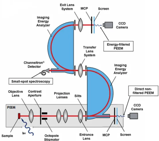
In our work we have employed a state of the art XPEEM spectromicroscope, the N anoESCA (from Omicron Nanotechnology), equipped with an aberration-corrected (double analysers) energy filtering system and multiple available laboratory photon sources: a monochromatic focused X-ray source (FXS) and three available UV and VUV photon sources (Hg, D2 and He discharging lamps). A preparation chamber connected to the microscope is also available for surface treatments under UHV conditions (Ar+ ion sputtering, resistive heating at high temperature)
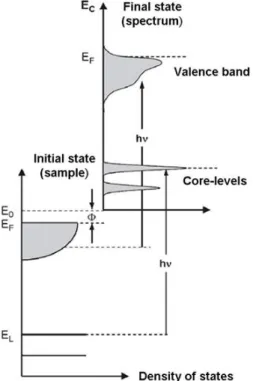
N anoESCA allows different imaging modes providing microscopic, spectro-scopic and spectromicrospectro-scopic measurements. Using XPEEM spectromicroscopy in the range of secondary electrons, the work function can be determined by measuring the emission threshold. Two dimensional maps of the work function
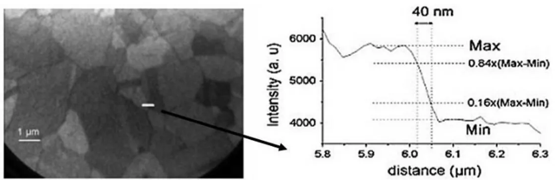
Figure 2.9: A PEEM image acquired using the N anoESCA spectromicroscope with an Hg (UV) photon source over a clean copper surface. The image of secondary electrons was taken at the energy of 4.4 eV, with a field of view of 15 µm. The spatial resolution of the secondary electron imaging was determined from the profile plot and evaluated at around 40 nm [9].
variations can be also obtained over the field of view (FoV) used in experiments (FoV between 20 to 600 µm are available with the N anoESCA). The study of the chemical and elemental composition of the surface is also possible with spectroscopic and spectromicrosopic measurements at core-level energies.
Figure 2.9 shows an example image acquired in XPEEM at the energy of secondary electrons of the same copper sample studied in KFM (see figure 2.8). The variation of the work function with the grains orientations is identified. The work function variations are measured with a 40 nm spatial resolution using an UV photon source.
complementarity of KFM and XPEEM...
It is our goal in this work to demonstrate the possibility of improving KFM measurements in air and to exploit the complementarity of KFM and XPEEM techniques as a way to attain high spatially resolved, reliable and reproducible measurements of the work function for newly developed technologies and materials.
In the next chapter, we will develop the working principles and used equipment of both KFM and XPEEM. In the last chapter, we will demonstrate an application of a coupled characterization protocol for the study of epitaxial graphene layers on SiC substrate.
Spatially resolved work
function mapping: principles
and methods
D
ans ce chapitre nous discutons en d´mesure du travail de sortie par les techniques de microscopie de forceetail les principes physiques de la de Kelvin (KFM) et de spectromicroscopie de photo´emission d’´electrons par rayons X (XPEEM). Les propri´et´es, avantages et limitations des micro-scopes utilis´es dans chaque technique seront aussi pr´esent´ees. Finalement, une comparaison sera ´etablie entre KFM et XPEEM en termes de fiabilit´e, r´esolution spatiale et compl´ementarit´e de la mesure du travail de sortie local.I
n this chapter we shall provide a detailed overview of the two principaltechniques of this thesis for the measurements of the local work function: the Kelvin Force Microscopy (KFM) and the X-ray Photo Electron Emission Microscopy (XPEEM). Key features addressed will include the principles of each technique as well as the properties, advantages and limitations of the equipment used in each measurement method. The KFM and XPEEM techniques will be compared in terms of reliability, spatial resolution, complementarity and direct measurement of the local work function.3.1
Kelvin Force Microscopy (KFM)
From a technical point view, KFM is an adaptation of an Atomic Force Microscopy (AFM) method to produce electrical measurements of the Contact Potential Difference (CPD) as measured by a classical Kelvin Probe (KP) instrument. Therefore, the description of the KFM technique requires a certain level of understanding of the working principle of AFM technique. We shall thus provide a description of some basic concepts of the AFM followed by a detailed description of the KFM principle and the equipment used in our experiments.
3.1.1 Atomic Force Microscopy: a brief introduction
The invention of the Atomic Force Microscopy in 1986 by Binning and Quate [56] was intimately linked to the invention of the Scanning Tunneling Microscopy (STM) in 1982 by Binning and Rohrer for which they received the Nobel Prize in 1986. The core of Atomic Force Microscopy (AFM) is formed by a sharp tip mounted on a flexible cantilever. While scanning the sample, the tip ’sees’ the surface as a field of interacting forces that disturb its equilibrium position. The detection of this disturbance and the regulation of the tip’s position actually form the basic signal of the AFM.
3.1.1.1 General principle
Unlike the STM, the conducting nature of the sample is not important in AFM. AFM can thus be used to study insulator, molecular as well as conducting surfaces. The AFM explores the interacting forces between the tip and the sample. Its basic application is to measure the topography of a given surface. However, depending on the nature of the interaction between the tip and the sample, the AFM is also capable of mapping various properties of the sample surface (i.e. viscoelastic, ferroelectric, electrostatic, magnetic and chemical properties), which opens the doors to a wide range of applications in the field of material science and characterization.
The operating principle and experimental setup Figure 3.1 represents of the experimental setup of an AFM microscope. The AFM probe is formed by a micro-sharp tip mounted on the end of a cantilever. While the tip interacts with the surface, the cantilever moves depending on the nature of the interaction force (i.e. repulsive or attractive). These movements are transfered to a four segment photodiode by means of a reflected laser beam at the end of the cantilever. An electrical current proportional to the laser beam movement is therefore created in the photodiode. This current is then converted into a voltage signal which is compared to a setpoint value dictating the desired position of the cantilever.
The error signal resulting from this comparison is then used to move the tip vertically in order to maintain the cantilever position at the setpoint value. The vertical movement of the tip is provided by a piezo-electric ceramic tube moving in the Z direction. The feedback procedure is ensured by an automatic regulation of the proportional and integral gains of a PID controller. The lateral scan of the tip in the (X, Y ) direction over the surface is provided by two additional piezo-electric ceramics. The height variations ∆Z, of the vertical piezo, forms the topography signal over the scanned surface Z(X, Y ).
The interacting forces between the tip and the sample Different types of interacting forces can be probed in AFM depending on the distance between
Figure 3.1: The general setup of a conventional AFM microscope.
the tip and the sample and their nature and composition. Forces have different intensities and ranges and can be classified into two main categories: attractive and repulsive forces.
Attractive forces Among the main attractive forces there are the van der Waals and Casimir forces resulting from the interaction of instantaneous dipoles. Capillarity forces caused by the formation of a water meniscus between the tip and sample in air resulting from a thin water layer on both surfaces (tip and sample). Electrostatic forces induced by the work function between a conducting tip and sample or from the presence of charges. For particular samples, magnetic or chemical forces can also be considered.
Repulsive forces Repulsive forces include the theories of elastic contact between solid bodies such as the Hertz theory and the Derjaguin-Muller-Toporov (DMT) theory. For interested readers, details can be found in [57].
The modes of operation In AFM techniques, two major modes can be distinguished: the contact mode and the oscillating or dynamic mode.
The contact mode The contact mode is the most intuitive mode which was demonstrated by Binning and Quate in 1986 [58]. The tip is brought into contact with the surface and changes of its deflection directly reflects the changes
of the surface topography. During an imaging procedure, the feedback loop maintains the deflection of the cantilever equal to a setpoint value by maintaining a constant f orce value along the scan.
The dynamic or oscillating mode In 1987, Martin, Williams and Wick-ramasinghe developed the use of the AFM with an oscillating tip at a very small distance above the surface [59]. They demonstrated a higher sensitivity when the cantilever oscillates at its resonance frequency. The amplitude, the resonance frequency and the phase shift of oscillations connect the dynamics of the vibrating tip to the tip-surface interactions. Any of them could be used as a feedback signal to track the surface’s topography. Due to the absence of contact, this mode is rather damages-less for both the tip and the surface. In the case of KFM experiments, we are actually interested in one particular dynamic AFM mode known as the Tapping mode.
3.1.1.2 The Tapping mode
In this mode, the cantilever is mechanically driven by a piezo-electric actuator, very close to its resonance frequency with an oscillation amplitude of several nanometers. During an oscillation, the tip undergoes intermittent contacts with the surface of the sample, hence this mode is known as the intermittent contact mode or Tapping mode.
General principle Initially, the cantilever is driven to oscillate freely, at its resonance frequency, far from the surface of the sample in order to avoid any interaction with it. When the tip-sample distance decreases, the tip starts feeling the variation of the gradient of the interacting force with the surface. This induces variations of the oscillation resonance frequency depending on the nature of the interacting forces (i.e. attractive or repulsive).
This leads to the variation of the initial (free) amplitude of oscillation of the cantilever. It also induces the variation of the phase delay between the cantilever’s stimulation signal and its actual oscillation. In Tapping mode, the amplitude of oscillations is often used as the feedback signal. The feedback loop keeps the amplitude constant (equal to a set point value) by maintaining constant the gradient of the interacting force.
An insight into the tip motion: amplitude and phase A thorough understanding of the Tapping mode operation requires solving the motion equation of the cantilever-tip ensemble under the influence of the tip-surface forces. A complete and rigorous approach involves the solution of the motion equation of a three dimensional vibrating cantilever. Although this approach is rather difficult, interested readers can find more details by following the works of Butt and Jaschke [60], Sader [61] and Stark and Heckl [62].

![Figure 3.8: An example of KFM lift mode imaging of clean copper surface [10]. The topography image (a) shows the copper grains of different crystallographic orientations which exhibits a V dc contrast (image b) measured in the second trace (lift)](https://thumb-eu.123doks.com/thumbv2/123doknet/12728346.357169/61.892.166.728.201.603/figure-topography-different-crystallographic-orientations-exhibits-contrast-measured.webp)
![Figure 3.14: Schematic of an electron microscope in LEEM and PEEM modes. The magnetic sector field allows detection of the reflected and photoemitted electrons respectively [76].](https://thumb-eu.123doks.com/thumbv2/123doknet/12728346.357169/71.892.251.639.313.612/schematic-electron-microscope-detection-reflected-photoemitted-electrons-respectively.webp)
![Figure 3.15: Schematic of a fully electrostatic PEEM column. Contrary to figure 3.14, the sample is close to ground and the extraction lens is at high voltage [86].](https://thumb-eu.123doks.com/thumbv2/123doknet/12728346.357169/72.892.210.672.590.866/figure-schematic-electrostatic-column-contrary-figure-extraction-voltage.webp)
![Figure 3.18: Energy level diagram illustrating the determination of the work function [90].](https://thumb-eu.123doks.com/thumbv2/123doknet/12728346.357169/77.892.171.482.424.723/figure-energy-level-diagram-illustrating-determination-work-function.webp)