HAL Id: hal-02383374
https://hal.archives-ouvertes.fr/hal-02383374
Submitted on 14 Jan 2020
HAL is a multi-disciplinary open access
archive for the deposit and dissemination of
sci-entific research documents, whether they are
pub-lished or not. The documents may come from
teaching and research institutions in France or
abroad, or from public or private research centers.
L’archive ouverte pluridisciplinaire HAL, est
destinée au dépôt et à la diffusion de documents
scientifiques de niveau recherche, publiés ou non,
émanant des établissements d’enseignement et de
recherche français ou étrangers, des laboratoires
publics ou privés.
The promise of antireflective gold electrodes for
optically monitoring the electro-deposition of single
silver nanoparticles
Jean-François Lemineur, Jean-Marc Noël, Catherine Combellas, Dominique
Ausserré, Frederic Kanoufi
To cite this version:
Jean-François Lemineur, Jean-Marc Noël, Catherine Combellas, Dominique Ausserré, Frederic
Kanoufi. The promise of antireflective gold electrodes for optically monitoring the electro-deposition
of single silver nanoparticles. Faraday Discussions, Royal Society of Chemistry, 2018, 210, pp.381-395.
�10.1039/c8fd00037a�. �hal-02383374�
The promise of antireflective gold electrodes for optically
monitoring the electro-deposition of single silver nanoparticles
Jean-François Lemineur,a Jean-Marc Noël,a Catherine Combellas,a Dominique Ausserreb and Frédéric Kanoufi*aThe interest in nano-objects has recently dramatically increased in all fields of science and electrochemistry is no exception. As a consequence, in situ and operando visualization of electrochemical processes is needed at the nanoscale. Herein, we propose a new interferometric microscopy based on antireflective thin metal electrode layer. The technique is coupled to electrochemistry in a model example: the electro-deposition of Ag metallic nanoparticles (NPs). This challenges the current opto-electrochemical methods and even those relying on nano-impact detection. Indeed, the sensitivity allows the dynamic in situ visualization of the electrochemical growth and dissolution of individual Ag NPs, whose size was tracked dynamically so far down to 15nm in diameter. The use of microelectrodes provides interesting quantitative analysis of the NPs, from optically resolved arrays of single NPs to condensed arrays of (unresolved) NPs. Particularly, the optical analysis of all the individual NPs allows the reconstruction of optical voltammograms similar to the electrochemical ones. Finally, the NPs dissolution-redeposition is also investigated.
Introduction
Many nanoparticles (NPs) are now employed for electrochemical detection1, electro-catalysis2,3, energy conversion4,5, etc. They all possess distinct characteristics, which make them unique, even within the same batch. In order to better understand the behaviors of NPs and to establish accurate structure-property relationships, it is essential to study NPs at the single object level.
Unfortunately, classical electrochemistry cannot reach this ultimate detection limit and only gives access to a current averaged over a large population. That is the reason why researchers are now turning towards nano-electrochemical studies at the level of individual nano-objects.6 This recent discipline has developed thanks to the invention of the scanning electrochemical microscope7 (SECM) and electrochemical tools such as nano-electrodes8, nano-pipettes9 and nano-confined electrochemical cells10. However, measuring the current related to one single NP remains challenging when size approaches the 20-nm range. Indeed at such scale the current to be measured, even when amplified by large turn-over-frequency catalytic reactions, is below few fA and NPs are difficult to manipulate individually. An alternative strategy consists in coupling electrochemistry to complementary microscopy techniques that are able to characterize the heterogeneity of electrochemical processes.11 Optical microscopies possess several advantages such as easier implementation and sample preparation than in situ TEM, high throughput imaging, in situ and operando monitoring and high spatial resolution.
Several optical microscopy techniques have already been successfully coupled to electrochemistry. The groups of Tao and of his collaborators12-14 used the surface plasmon resonance microscopy (SPRM) to image different electrochemical processes occurring at individual nano-domains or NPs. Particularly related to the present work, they demonstrated the ability to image the electro-dissolution of single silver NPs.15 The technique takes advantage of the sensitivity of plasmon (a collective oscillation of the conduction electron) generated on a thin gold electrode to local
variations of the refractive index.16 When a NP is present on the gold surface, it locally changes the refractive index and it is detected easily with a high sensitivity. When NPs catalyze a reaction, the formation of products can also be monitored through the ability of either the products or reactants to induce a local refractive index change, allowing a quantitative imaging of electro-catalytic reactions at the single NP level.17
Similarly, noble metal NPs support a localized surface plasmon resonance (LSPR) when they are illuminated in the visible region.18 As the LSPR is function of the size19, the shape20 and the surrounding medium21 of a NP, it can also be used to monitor the electrochemical behavior of single NPs. The light scattered by the NPs carries such chemical information, which can be collected by means of an inverted microscope in a dark-field configuration. This opto-electrochemical setup was proposed for the first time by Hill and Pan to follow the electro-deposition of silver NPs.22 Moreover, different implementations can be added to such dark-field microscopes allowing for example to afford spectroscopic analyses of the scattered light, again at the single NP level, in order to provide complementary chemical or size information.23-27 Moreover, our group has developed a three dimensional dark-field approach, which allows tracking NPs during stochastic collision with an electrode.28
However, the present optical techniques are limited to the detection of (often plasmonic) nano-objects larger than 30-40nm. They are thus so far providing complementary information to the direct electrochemical detection of single NP, without truly pushing the limit of their electrochemical detection. Extending the sensitivity of electrochemical detection is often provided through differential measurements (e.g. differential pulse voltammetry) allowing to reduce the signal-to-noise ratio. Similar strategy applies to optical detection, and differential optical measurement is afforded by interferometric detection, through the observation of constructive or destructive interference patterns. In this respect, the iSCAT29 method relying on such principle is based on an interference phenomenon between the light scattered by a NP and
the light reflected at the interface of a glass substrate. The technique extends the sensitivity of current direct dark-field observation as the optical signal scales linearly with the NP volume (rather than its square-volume in the case of direct dark-field microscopy) and allows visualizing NPs as small as 5nm in diameter.30 Unfortunately, interferences occur at the water/glass interface and substrates cannot operate as working electrodes. Transposing this concept to a solution-metal electrode interface under backside optical observation would require that, upon backside observation, the metal-coated substrate presents antireflection (AR) interference properties to extinguish the reflected light properties (through destructive interferences) to significantly increase the signal-to-noise of processes occurring at the solution-metal interface. However it was long thought that AR conditions could not be reached with highly absorbing, such as metallic, layers deposited on transparent (e.g. glass slide) substrate. It was recently demonstrated, that this could be achieved by considering absorbing AR layers of thicknesses much lower than the wavelength, typically down to few nanometers. Such AR layers made of gold on glass are thus ideal for opto-electrochemical studies. Their optical observation is made in the so-called Backside Absorbing Layer Microscopy (BALM)31 and we demonstrate herein how it can be implemented to follow and analyze quantitatively the electrochemical growth/dissolution of Ag NPs at an ultra-microelectrode (UME) surface.
Results and discussion
Opto-electrochemical setup
The BALM technique operates thanks to a highly absorbing and AR layer deposited at the surface of a glass slide. The AR properties are due to destructive interferences between beams reflected at the two AR layer interfaces: the glass-AR and AR-solution (or AR-air for observation in air) interfaces. The light extinction only appears if the substrate is lighted from the face of higher refractive index (glass in our case).31
Practically, the extinction conditions are approached by using a ~ 5nm thick layer of gold deposited on a glass slide of 0.5mm. The substrate is mounted on an inverted microscope and is illuminated from the glass by a white LED through a 63x immersion objective. The reflected light is collected by the same objective and is sent to a 8-bit color CCD camera, giving a color image. The BALM intensity on each pixel can be analyzed quantitatively, either from an overall intensity, IBALM, directly measured at a pixel location on the RGB
(red, green, blue) image. The intensity can also be averaged over a region of fixed area (typically 4x4 pixels, with 1pixel = 0.11µm). The averaged intensity is then named <IBALM>. For higher sensitivity and
detection of smaller size NPs, the RGB image can be split into three distinct images recorded on the red, blue and green channels. The most sensitive channel is the G one, the intensity measured in this channel is denoted IB,G.
For the electrochemical setup, the gold layer is used as a working electrode in a three-electrode system connected to a potentiostat.
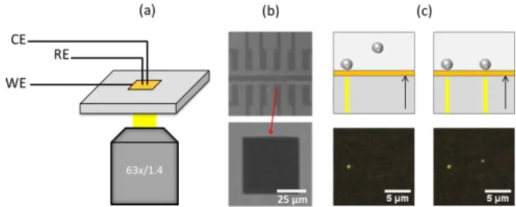
Platinum and silver wires serve as counter and pseudo-reference electrodes, respectively. The opto-electrochemical setup is schematized in Figure 1a. Ultra-microelectrodes (UME) were lithographed from the gold surface and served as individual electrochemical cells. Figure 1b shows the network of twelve electrodes printed on the glass substrate and a 50x50µm² UME localized at the center of each electrode, which is the only part in contact with the solution. The rest of the gold electrodes is covered by an insulating silicon nitride coating.
Figure 1: Schematic representation of the opto-electrochemical setup designed to study the oxidation-reduction of silver NPs (a). Optical microscopy images (b) of twelve electrode array printed on the AR layer and of the UME localized at the center of each electrode. Schematic representation (top) and BALM images (bottom) of silver NPs immobilized on the UME that destroy the extinction properties of the AR layer (c). When a nano-material lies on the substrate, it modifies the extinction properties of the AR layer and some of the light is locally reflected. An example is schematized in Figure 1c. Two BALM images were extracted from a video recorded during stochastic collisions of colloidal citrate-capped silver NPs (100nm) with the AR electrode. In the first BALM image, a NP is already present on the AR surface. After a certain period of time, a second NP lands on the electrode surface. The two NPs locally disrupt the destructive interferences between reflected beams and thus appear highly contrasted.
As will be discussed later, these calibrated colloidal Ag NPs can be used as reference systems both for optical calibration of the NP size, and for comparison of the electrochemical reactivities of electrodeposited and surface-capped NPs.
Optical monitoring of Ag NP growth and dissolution
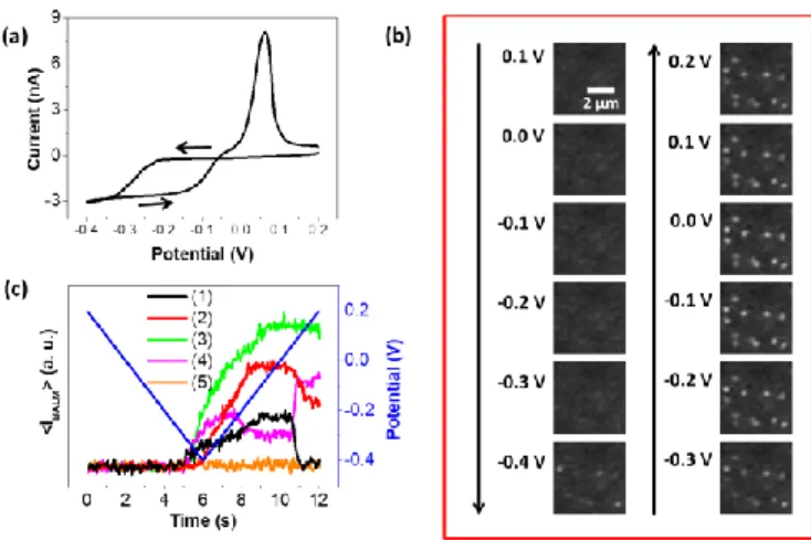
A typical example of growth and dissolution of silver NPs is presented in Figure 2. A cyclic voltammetry (CV) is carried out at the UME with the opto-electrochemical setup, in a potential range of 0.2 to -0.4V. The aqueous solution employed was composed of 200M AgNO3 and 0.1M NaNO3. During the potential sweep, the
total electrochemical current at the UME is recorded (Figure 2a). It increases sharply after -0.25V and reaches a stationary value, -3nA, indicating that when the potential is reductive enough (E<-0.35V on the forward sweep) the Ag electro-deposition becomes controlled by mass-transfer to the UME as the value is in good agreement with the mass-transfer limited reduction of Ag+ to a squared UME28 (iUME
= nFCDa/21/2 which for a=50 µm and D=1.6x10⁻⁵ cm2/s yields 3.5nA). The onset of Ag+ reduction is however significantly delayed, suggesting a strong kinetic inhibition of the process, which suggests, from the electrochemical measurement, that the UME most likely behaves as a partially blocked electrode32 and that the reduction of
Ag+ is most likely effective on distant active nano-domains. The distance between these active nano-domains is sufficiently large so that they behave as independent and non-overlapping nanoelectrodes, until the UME masstransfer control is reached at -0.35V. As the reduction of Ag+ is expected to electrodeposit Ag NPs, both the UME surface coverage and the dimension of the nano-domains (dictated by the Ag NPs size) are expected to increase while E is made more cathodic. At some point the diffusion layers between neighboring Ag NPs are overlapping and the reduction process is then governed by the mass-transfer to the UME. On the backward sweep, the current trace crosses over the forward one. This is expected to occur in potential regions closer to the value of the E0 for the reversible Ag+/Ag transformation. Typically, the E0 value of the overall process can be estimated from the point where both traces are crossing, here -0.06V vs AgQRE. A clear oxidation peak centered at 0.05V can also be noted on the backward sweep, corresponding to the re-oxidation of metallic silver. The charge quantity associated to the reduction of Ag+ is higher than that related to the oxidation of Ag0 indicating that the NP dissolution is partial.
In the same time, BALM optically monitors the electrochemical events occurring over the entire gold UME surface. Several BALM images taken from a part of the UME at different potentials are presented in Figure 2b. They have been extracted from the video recorded during the optical monitoring of the CV. It can be noted that bright spots, assigned to silver NPs, appear when ~ -0.3V is reached. The nucleation and growth of the NPs result from the reduction of silver ions into metallic silver atoms. The images shown in Figure 2b also qualitatively confirm the partially active UME behavior postulated from the electrochemical trace. Indeed, in the images taken at -0.3 and -0.4V on the forward scan, two to four NPs are generated separated by ca. 2µm, agreeing with the hypothesis of Ag NPs behaving as independent nano-electrodes. On the reverse scan, the NP density significantly increases, as up to 12 NPs are detected in the images, also with apparent higher BALM intensity and therefore, as will be shown below, larger sizes. This density is also in agreement with the possible overlapping of nano-electrodes, expected for such density for NP dimensions of the order of 10-100nm.33,34 When the potential comes back to more anodic regions, the optical intensities of many, but not all, NPs are decreasing, which also confirms the partial dissolution of NPs. Since the CV shown in Figure 2a is an overall measurement of the growth and dissolution of hundreds of NPs, it is impossible to isolate the electrochemical behavior of individual NPs. In order to get access to this information, we rather exploit BALM intensity transients extracted from the video recorded during the CV. They are built by measuring the average pixel intensity, denoted <IBALM>
in a 0.44x0.44 µm2 region where a NP is detected as a function of time or applied potential.
Figure 2: Optical and electrochemical monitoring of a CV in a potential range of 0.2 to -0.4V at a rate of 0.1V/s. The aqueous solution was composed of 200µM AgNO3 and
0.1M NaNO3. Total electrochemical current (a) recorded at the UME during the cyclic
potential sweep. BALM images of ~ 5.5x5.5 µm2 region of the UME (b) extracted from a
video recorded during the CV and at several potentials. (c) Time-intensity transients constructed by measuring the average pixel intensity, <IBALM> in 0.44x0.44µm2 regions
where a NP is present. The time-intensity transient labeled as (5) corresponds to an electro-inactive area and is thus considered as the variation of the background. Distinct electrochemical events were optically observed during the cyclic potential sweep. They are summarized in Figure 2c. In the first three (1-3) cases, the dissolution processes seem different. In transient (1) the NP grows on the UME and entirely dissolves during the anodic scan. In transient (2), the NP is formed on the electrode surface but only partially dissolves. In transient (3), the NP does not oxidize at all when the potential goes back to positive values. Three hypotheses can be advanced to explain these dissolution heterogeneities. A passivating oxide layer can quickly form at the NP surface, which partially or totally inhibits oxidation. This point has been recently addressed by the Willets’ group.27 In a second time, the NP dissolution rate could be influenced by local variations in the NP surface coverage and NP size. As explained by Compton and co-workers, the ion diffusion from the electrode resulting from the NP dissolution must be taken into account.35 If the NP surface coverage or the NP size locally changes, the ion mass-transport may vary, leading to variations in the dissolution rate of NPs. Finally, the NP size can also influence the NP standard electrode potential:36,37 when the NP is smaller, the surface free energy is more important and the NP oxidizes faster. Other time-intensity transients (such as in (4)) are also obtained, expressing more complex processes as partial desorption, or multi-step growth/dissolution. Similarly to the oxidation, heterogeneities can also be found during the electro-deposition. Some NPs grow before and/or faster than others for similar reason.
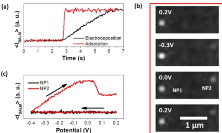
Figure 3: Differentiation of the NP reduction process and the NP surface chemistry. (a) Time-intensity transients recorded with BALM for a NP adsorption (red) and a NP electrodeposition (black). (b) BALM images recorded during a CV between 0.2 and -0.4V. Potentials at which images were extracted are incrusted in the Figure. Citrate capped silver NPs and electro-deposited NPs are labeled as NP1 and NP2, respectively. (c) Potential-intensity transients of NP1 and NP2.
The optical coupling can also be used to distinguish two possible mechanisms of NP formation. It is well known that silver nitrate solutions are photosensitive and that silver ions are occasionally reduced to metallic silver when exposed to visible light.38,39 Some NPs present on the UME surface can thus be the result of a photo-reduction mechanism rather than an electrochemical process. Fortunately, NPs arising from these two different processes do not appear on the same time scale at the UME surface. Time-intensity transients of two NPs, one of which is formed by photo-reduction and the other one by electro-reduction, are presented in Figure 3a. The photo-reduction is believed to occur in solution as a part of the light used to illuminate the sample is expected to be transmitted to the solution phase. After its formation, the photo-reduced NP diffuses into the solution and eventually adsorbs at the UME surface in a fraction of second. The NP can even be tracked a little bit before its immobilization. Conversely, the electro-reduction of Ag+ into electrodeposited Ag NP takes place at the electrode surface and the growth of the NP can last few seconds. The comparison of the time scales allows differencing these two reduction processes.
BALM also allows investigating the difference of reactivity between NPs. It is illustrated here by the adsorption of Ag NPs (100nm in diameter) capped by citrate ligands at the UME surface by immersion into a solution of ~ 10pM prior to the CV. The electrochemical reactivity of citrate capped NPs was then compared to that of NPs generated during the cathodic scan (Figure 3c). Almost no variation in the optical intensity is detected for citrate-capped NPs. Findings are identical for all citrate-citrate-capped NPs present on the UME surface. It means that under our experimental conditions, citrate-capped silver NPs do not act as nucleation sites and do not grow during the cathodic scan. They do not oxidize either at the applied anodic potentials. A significant effect of the capping agent on the NP oxidation was also evidenced by stripping voltammetry of Ag NPs.40 The charge from the anodic stripping peak is thus fully made of the dissolution reaction of freshly electrodeposited NPs.
Quantitative analyses and sensitivity
The BALM intensity is higher when the NP is larger. A linear relationship between the NP volume and the background-subtracted intensity was demonstrated in previous work.41 Thanks to such empirical law, the size of the NP is accessible throughout the potential sweep. The relationship between the BALM intensity and the volume of electrodeposited Ag NPs determined by SEM (Figure 4a, same location for SEM and BALM) is also linear and comparable but actually less sensitive, than that observed previously (slope <IBALM>- 41 Indeed,
the condition for light extinction from the AR absorbing layer strongly depends on the Au layer thickness which is ~ 5nm. Slight variation, from batch to batch, of this thickness is thus expected inducing both changes in the signal-to-noise ratio and in the extent of constructive or destructive (extinction) interferences and therefore in . Moreover, SEM images also show sometimes bulb-like NPs whose volume may be delicate to accurately estimate. In order to quantify NP size variations from BALM measurement during a full reduction-oxidation process, without recoursing to SEM imaging, an alternative consists in referring to gauge NPs of known size immobilized on the AR substrate. This was obtained by adsorbing colloidal citrate-capped NPs, here of 100nm diameter as mentioned in Figures 1 or 3b,c on the AR surface. The unknown size of the electrodeposited NPs was then inferred, as in (1), by comparing the <IBALM> values of both gauge and electrodeposited
NPs and assuming a linear relationship with the NP volume (V). VNP = Vgauge <IBALM,NP>/<IBALM,gauge> or VNP = <IBALM,NP>/
As an example, size dispersion graphs were constructed from two BALM snapshots taken at two different potentials during the forward potential scan. It can be clearly noticed from the size distributions in Figure 4b that the mean NP diameter increases before the oxidation peak from 46±15nm at a potential of -0.40V to 75±8nm at -0.05 V.
Figure 4: Quantitative information deduced from the BALM intensity. (a) Background-subtracted BALM intensity as a function of the NP volume measured by SEM. Inlays are two correlated SEM and BALM images in the same electrode area. The linear fit of the data (N=20) is shown in red (R=0.95). (b) Size dispersion graphs of the electro-deposited NPs at a potential of -0.40 (red) and -0.05 V (blue). (c) Optical cyclic voltammetries of individual Ag NPs, whose diameters reach ~ 36, 72 and 102nm at the end of the growth step. (d) Total current at the UME calculated from optical data as a function of the applied potential (compared to the electrochemical current in black). Once the size of an individual NP is known at every potential value, the current related to the growth/dissolution of an individual NP, iNP, can be estimated from the molecular volume of Ag (Vm,Ag =
10.27 cm3/mol) through the Faraday law (2).22 As an example, the currents generated by the oxidation/reduction of single NPs with diameters of 36, 72 and 102nm are plotted in Figure 4c as a function of the applied potential, giving rise to a so-called optical cyclic voltammetry.
iNP = F/Vm,Ag dVNP/dt (2)
Moreover, the UME is entirely imaged by the microscope as it is micrometric. Therefore, optical data give access to the total number of NPs at the electrode surface, even though they may not be all resolved individually, together with the size of each individual NP at any potential value. By cumulating the information of each NP (N~650 on the UME), the amount of matter present at the UME and optically addressable at any step of the CV can be estimated by using equations (1) and (2). This amount relies on the local estimate of NP volume on different sub-regions of the electrodes defined by thresholding the optical images and estimating <IBALM> in the
different threshold regions. Typically, some regions of the electrode are densely covered by NPs and this strategy likely underestimates the deposited amount of material. However an estimate of the overall Faradaic current related to the growth and dissolution of all the individual NPs and individual domains detected is estimated at different potential steps and presented in Figure 4d. The shape of overall optically-inferred voltammogram perfectly matches that of the actual electrochemical voltammogram in Figure 2a. However, the optically inferred current amplitude -0.7nA from the monitored UME is ~ 5 times smaller the current expected for the mass transfer limited current detected electrochemically. It suggests that the analysis either is blind to a number of large domains or the simple linear IBALM-VNP relationship imperfectly quantifies these large
domains containing large NPs.
Resolution and sensitivity
The lateral and vertical resolution of the BALM microscopy was evaluated by the average optical intensity of NPs (100nm diameter) adsorbed at the gold surface.
Figure 5: Sensitivity and resolution of the BALM. (a) Intensity profile (G channel) of a 100nm colloidal Ag NP adsorbed at the UME surface; the profile is fitted with a Gaussian profile (blue line) accounting for the point-spread-function, defined by its maximum intensity and FWHM. (b) Intensity-time transient (G channel) of a NP electro-generated at the UME. The dashed line represents the vertical limit of detection. (c) Intensity-time transient of a presumably large nano-domain (0.44x0.44 m2) correlated
with the variation of its FWHM; the variation of the FWHM of a 100nm-adsorbed NP is also provided in (c).
As shown in Figure 5a, from a line plot over a NP on an image analyzed in the green channel of the CCD camera, which appears more sensitive to small NPs, the maximal optical intensity of the
NPs, IB,G, amounts to 188±12, while the average <IB,G> measured
over a 0.44x0.44µm2 region is 126±23. The dashed line in Figure 5b shows the limit of optical detection (LOD) during the electro-deposition of a NP. By using the average relative intensity of the absorbed 100nm NPs as a calibration value, we estimate the limit of detection represented by the arrow point in Figure 5b to a NP with a diameter of ~ 20 nm. This strategy reproduced for various NPs show that the sensitivity is of the order of 15 nm as suggested by the size distribution presented in Figure 4b.
By optimizing the gold layer thickness as well as the video acquisition parameters, NPs <10 nm were observed.41 It is also important to point out that the optical setup (a classical inverted microscope, a white LED and a standard 8-bit color CCD camera) is quite common. Then, there are still rooms for improving the opto-electrochemical setup and thus having a better sensitivity, which could theoretically reach nanometer scale vertical resolution.24 The line plot in Figure 5a also provides estimate of the resolving power of the BALM microscopy. The profile can be fitted by a Gaussian profile, approximating the expected Airy disk revealing the diffraction-limit optical visualization of a point source. The full-width at half-maximum (FWHM) of the Gaussian fit is 360±10nm. It is in good agreement with the expected value for the microscope objective of numerical aperture, NA=1.4, for which Abbe condition for lateral resolution yields FWHM = /2NA, that is 370nm for an average 520nm wavelength, . As discussed above, some regions of higher intensities may present several NPs whose size may be difficult to quantify from the simple linear relationship (1). These regions can then be distinguished by super-localizing their lateral dimension during the electro-deposition process. If a single diffraction pattern is observed for such apparently large Ag nano-domain, its line profile can be fitted by a Gaussian (as in Figure 5a). The evolution of the FHWM of the Gaussian fit, along with the apparent nano-domain dimension from eq (1), as a function of time are provided in Figure 5c for a presumably large Ag nano-domain. If the nano-domain is definitely diffraction limited at the earliest stage of the growth a clear increase (resp. decrease) of the FWHM is observed when the nano-domain is increased (resp. decreased). For reference, the FWHM of a 100nm gauge NP is constant during the overall process. The latter confirms that the electro-deposition does not proceed on the citrate-capped NPs. The former change in FWHM is not expected for the direct observation of 100nm NPs, which should be diffraction limited. It strongly suggests that the lateral growth of the domain during the electro-deposition is monitored. It can be attributed to the growth from two separate nuclei, which cannot be resolved, but are manifested through an apparent variation of 20nm in FWHM. This shows however to what extent the direct measurement of the ensemble response from the individual optical response is complementary and may be misleading for absolute quantification.
Toward more complex surface processes
To illustrate the issue associated to the optical resolution of dense arrays of NPs, electro-deposition allows also the control of NP density on the electrode. The UME used in the previous section
presented likely some regions contaminated by organic layers responsible for the strong kinetic inhibition of the Ag+ reduction. It is owing to some difficulties in efficiently cleaning the UME after photoresist insolation without affecting the quality of the Au layer. Here, we then returned to larger electrode (disk of ca. 350µm diameter) while higher NP surface coverage was obtained by using higher Ag+ ions concentration.
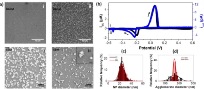
The stripping of small silver NPs and their further reduction was monitored. Firstly, a dense monolayer of NPs was electro-generated at the AR electrode surface from an aqueous solution composed of AgNO3 (250µM), NaNO3 (0.1M) and sodium citrate (5mM). The
citrate was added to promote the nucleation of NPs and to avoid their excessive growth. SEM analysis shows NPs of 25±6nm diameter (as provided in Figure 6a) with an important surface coverage of ~ 350NPs per µm2. At such high density, NPs cannot be resolved individually by optical microscopy, because the inter-NP distances are smaller than the diffraction limit. Such NP monolayer, from the point of view of optics, is however easily detected in BALM as it corresponds to a marked increase in the average optical intensity of the AR electrode. From the average BALM intensity (background subtracted) recorded on such surface, <IBALM>=35, and
assuming the proportionality law (1) observed in Figure 2a, a=5x10⁻⁵ nm-3, one can estimate an average volume of Ag of ~ 7x10⁵nm3 over a 0.44x0.44µm2 region, yielding, for the estimated 25nm NPs of individual volume 8x10³nm3, an approximate density of 440 NP/µm2 in rather good agreement with that estimated from the SEM image. It then suggests that BALM may also be used to quantitatively analyze NP surface coverage for homogeneously coated surfaces.
A cyclic potential sweep was performed immediately after the NPs formation from -0.6 to 0.6V. The resulting optical CV (Figure 6b) can be interpreted as a classical electrochemical CV of an ensemble of NPs. The NPs oxidation occurs at ~ 0.05V, which is in agreement with the CV in Figure 2a. Almost all NPs disappear from the electrode surface at the exact same oxidation potential. Here the electrode is much larger than the optically monitored area, it is therefore delicate comparing both optically inferred current and the electrochemical one. However they both have very similar shapes. The charge exchanged, 2.6µC, for a ca. 0.1mm2 electrode would correspond to a partial oxidation of the ca. 440 NP(of 25nm)/µm2, even though the optical signal is going back to noise level, suggesting that all NPs have been removed from the electrode (at least the optically monitored region).
On the reverse cathodic sweep, and as observed before at the UME, the reduction of Ag+ is optically detected at -0.25V. Interestingly, rather than a homogeneous layer of NPs, brighter and well resolved spots appear at the electrode surface, indicating a significant change in the structure of the silver NP layer.
Figure 6: In-situ monitoring of NP stripping and further reduction. (a) BALM and SEM images recorded at the beginning (i) and at the end (ii) of the potential sweep from -0.6 0.6 -0.6 V. The inlay is the SEM image of (ii) is a zoom showing the NP agglomerates. (b) Optical CV obtained by differentiating <IBLAM> (over a 0.44x0.44 m2)
as a function of time. (c) Size dispersion graphs based on SEM analyses of the electro-deposited NPs at the beginning (i) and at the end (ii) of the potential sweep. (d) Comparison of the sizes of the agglomerates measured in SEM (black) and in BALM (red).
Based on the dispersion and the intensity of the spots, the forward potential scan seems generating more separated NPs with a mean diameter of 166±8nm based on their individual BALM intensity. Ex situ SEM analyses (Figure 6a, lower right) show that the bright spots detected by BALM are agglomerated NPs. These agglomerates have a measured mean diameter of 173±41nm, which is in good agreement with the diameter deduced from the individual NP BALM intensities (Figure 6d). In addition, the NPs, which compose these agglomerates, have the same diameter as the NPs in the initial monolayer (25±6nm on average, Figure 6c, based on SEM analyses).
Interestingly, similar in situ experiments with lower electrode surface coverage do neither give rise to the total disappearance of NPs, nor to the formation of NP agglomerates. As reported, the silver NP dissolution during oxidation is generally partial.27,40 Consequently, the monolayer vanishing can be attributed to electrochemically assisted desorption of NPs when the surface coverage is high enough. During the backward cathodic scan, partially electrodissolved NPs re-adsorb at the AR electrode surface and re-grow in the form of agglomerates. Alternatively, the dissolution step of the NPs induces a local increase of Ag+ concentration in the vicinity of the substrate, potentially impacting the growth process of the NPs during the second scan. Indeed, previous work evidenced significant modifications of the NP shape induced by metal ions concentration.42
Experimental
Chemical
All chemicals were obtained from Sigma-Aldrich and were of analytical grade. Ultra-pure water with a resistivity >18.2MΩ cm was used to prepare all solutions.
Opto-electrochemical setup
The gold AR substrates were purchased from Watch Live SAS and placed on a Zeiss Axiovert.A1 inverted microscope equipped for BALM observation by Watch Live SAS. The substrates were illuminated from the higher refractive index
(glass) face though a 63x oil immersion objective with a numerical aperture of 1.40. The light was polychromatic and unpolarized. The gold film was used as the working electrode together with a 50µm diameter platinum wire and a 500µm diameter silver wire serving as counter and pseudo-reference electrodes, respectively. Electrochemical experiments were performed on a CHI 760 potentiostat connected to a computer. During the potential sweep, videos were recorded at 20 frames per second by a CCD 8-bit color camera. Electrochemical cells were machined in house from plastic, as reported previously.41 The UME was lithographed directly from the gold layer deposited on the glass substrate.
UME network fabrication
The UME fabrication was conducted in clean room facilities. First, a negative photosensitive resin was spin-coated at the gold surface and the electrode network was printed by UV light illumination through a mask. The pattern was then developed by immersion in a developing solution. After that, the unprotected gold layer was etched by plasma, leaving only gold covered by the resin. It gave rise to an array of twelve electrodes printed on the glass substrate, as presented in Figure 1b. The resin was removed by soaking the sample generously in acetone and isopropanol.
The next step was to delimit an UME on each electrode surface, which will be the only part in contact with the solution. The glass slide was covered with an insulating layer deposited by chemical vapor deposition. This time, a positive resin was spin-coated at the substrate surface and only 50x50µm² squares localized at the center of each electrode were not exposed to UV light. Then the resin was developed and the insulating layer was etched by plasma treatment in the unprotected area letting appear small gold squares (the UMEs). The rest of the resin was removed by soaking the sample in acetone and isopropanol. The ends of the electrodes were finally attached individually to metallic wires by conductive glue and connected to a potentiostat for electrochemical experiments.
Conclusions
A simple opto-electrochemical setup, based on backside absorbing layer microscopy (BALM) is described and proposed to monitor nano-electrochemical processes occurring at an electrode surface. BALM offers a high sensitivity as it relies on an interferometric detection and could theoretically reach sub-nanometer scale vertical resolution in the optimal experimental conditions.
Coupled to lithographed ultra-thin UME arrays, it was used to track in situ and operando the electrochemical growth/dissolution of Ag NPs at the single NP level with sensitivity as low as 15nm NPs in the present experiments, while 10nm was reached at an AR substrate of higher sensitivity. Interestingly, heterogeneities are evidenced in the electrochemical behavior of Ag NPs during both deposition and dissolution.
During the electrodeposition process, the opto-electrochemical setup allows discriminating electro-reduced Ag NPs from adsorbed NPs issued from photo-reduction in the bulk, and highlights the effect of a capping ligand at the NP surface on its electrochemical reactivity. The latter actually are not privileged site of further Ag0 growth. BALM also detects NPs aggregation at high electrode surface coverage during cyclic potential sweep. The growth from the UME surface is shown to proceed either from optically resolved nuclei acting as independent nanoelectrode, or from overlapping nanodomains, up to film of nanoparticles. These different schemes could be detected and to such point the amount of electrodeposited Ag material could be quantitatively analyzed by BALM, through a linear relationship between the BALM intensity and the NP volume, valid for both single NPs and dense films of small NPs.
The anodic dissolution of the electrodeposited NPs was also monitored confirming the occurrence of heterogeneous electrochemical behaviors, such as partial and complete NP oxidation, or more complex processes as partial desorption. The latter is particularly evidenced from the strong restructuration of a dense film of (unresolved) NP upon its oxidation/reduction yielding the redeposition of isolated aggregates.
If an UME is used, the whole electrode can be imaged and quantitative optical measurements be compared to the electrochemical one. If the overall optically-inferred and electrochemical voltammograms have very similar shape, the consideration of the optical signal recorded for all NPs seemingly underestimates the current exchanged during the electro-deposition. It is attributed to regions presenting higher densities of unresolved NPs. To such point, the concept of super-localization could be applied to show that in some regions the concomitant growth of two distinct NPs could be monitored.
BALM can be applied to any kind of nano-objects, making our opto-electrochemical setup a very versatile technique, which can also complement UME arrays. It could bring interesting perspectives such as multiple electrochemical analyses or implementation in micro-fluidic devices.
Conflicts of interest
There are no conflicts to declare.
Acknowledgements
The authors acknowledge funding by the Agence Nationale pour la Recherche (ANR) through the NEOCASTIP ANR-15-CE09-0015-02 project.
Notes and references
1 A. Chen,S. Chatterjee, Chem. Soc. Rev., 2013, 42, 5425– 5438.
2 Z.-Y. Zhou, N. Tian, J.-T. Li, I. Broadwell, S.-G. Sun, Chem. Soc.
Rev., 2011, 40, 4167–4185.
4 M. Shao, Q. Chang, J.-P. Dodelet, R. Chenitz, Chem. Rev., 2016, 116, 3594–3657.
5 S. Guo, E. Wang, Nano Today, 2011, 6, 240–264. 6 I. Valov, W. D. Lu, Nanoscale, 2016, 8, 13825–13827. 7 A. J. Bard, F.-R. F. Fan, J. Kwak, O. Lev, Anal. Chem., 1989, 61,
132–138.
8 D. W. M. Arrigan, Analyst, 2004, 129, 1157–1165.
9 M. Zhou, Y. Yu, K. Hu, H. L. Xin, M. V. Mirkin, Anal. Chem., 2017, 89, 2880–2885.
10 M. A. G. Zevenbergen, D. Krapf, M. R. Zuiddam, S. G. Lemay,
Nano Lett., 2007, 7, 384–388.
11 C. M. Hill, D. A. Clayton, S. Pan, Phys. Chem. Chem. Phys., 2013, 15, 20797–20807.
12 Y. Fang, H. Wang, H. Yu, X. Lui, W. Wang, H. Y. Chen, N. J. Tao, Acc. Chem. Res., 2016, 15, 2614–2624.
13 D. Jiang, Y. Jiang, Z. Li, T. Liu, X. Wo, Y. Fang, N. J. Tao, W. Wang, H. Chen, J. Am. Chem. Soc., 2017, 139, 186–192. 14 Y. Wang, X. Shan, H. Wang, S. Wang, N. J. Tao, J. Am. Chem.
Soc., 2017, 139, 1376–1379.
15 Y. Fang, W. Wang, X. Wo, Y. Luo, S. Yin, Y. Wang, X. Shan, N. J. Tao, J. Am. Chem. Soc., 2014, 136, 12584–12587.
16 B. Huang, F. Yu, R. N. Zare, Anal. Chem., 2007, 79, 2979– 2983.
17 X. Shan, I. Diez-Pérez, L. Wang, P. Wiktor, Y. Gu, L. Zhang, W. Wang, J. Lu, S. Wang, Q. Gong, J. Li, N. J. Tao, Nat.
Nanotechnol., 2012, 7, 668–672.
18 P. K. Jain, X. Huang, I. H. El-Sayed, M. A. El-Sayed, Acc. Chem.
Res., 2008, 41, 1578–1586.
19 S. Link, M. A. El-Sayed, Int. Rev. Phys. Chem., 2000, 19, 409– 453.
20 P. K. Jain, K. S. Lee, M. A. El-Sayed, J. Phys. Chem. B, 2006,
110, 7238–7248.
21 S. Underwood, P. Mulvaney, Langmuir, 1994, 10, 3427–3430. 22 C. M. Hill, S. Pan, J. Am. Chem. Soc., 2013, 135, 17250–
17253.
23 M. Chirea, S. S. E Collins, X. Wei, P. Mulvaney, J. Phys. Chem.
Lett., 2014, 5, 4331–4335.
24 V. Brasiliense, P. Berto, C. Combellas, R. Kuszelewicz, G. Tessier, F. Kanoufi, Faraday Discuss., 2016, 193, 339–352. 25 C. P. Byers, B. S. Hoener, W.-S. Chang, M. Yorulmaz, S. Link,
C. F. Landes, J. Phys. Chem. C, 2014, 118, 14047–14055. 26 C. P. Byers, B. S. Hoener, W.-S. Chang, S. Link, C. F. Landes,
Nano Lett., 2016, 16, 2314–2321.
27 V. Sundaresan, J. W. Monaghan, K. A. Willets, J. Phys. Chem.
C, 2018, doi:10.1021/acs.jpcc.7b11824.
28 V. Brasiliense, A. N. Patel, A. Martinez-marrades, J. Shi, Y. Chen, C. Combellas, G. Tessier, F. Kanoufi, J. Am. Chem. Soc. 2016, 138, 3478–3483.
29 J. Ortega-Arroyo, P. Kukura, Phys. Chem. Chem. Phys., 2012,
14, 15625–15636.
30 V. Jacobsen, P. Stoller, C. Brunner, V. Vogel, V. Sandoghdar,
Opt. Express 2006, 14, 405–414.
31 S. Campidelli, R. A. Khachfe, K. Jaouen, J. Monteiller, C. Amra, M. Zerrad, R. Cornut, V. Derycke, D. Ausserré, Sci. Adv., 2017,
3, 1–6.
32 C. Amatore, J. M. Savéant, D. Tessier, J. Electroanal. Chem.
Interfacial. Electrochem., 1983, 147, 39–51.
33 N. Godino, X. Borrisé, F.X. Muñoz, F.J. del Campo, R.G. Compton, J. Phys. Chem. C., 2009, 113, 11119-11125. 34 C. Adam, F. Kanoufi, N. Sojic, M. Etienne, Electrochim. Acta,
2015, 179, 45-56.
35 H. S. Toh, C. Batchelor-McAuley, K. Tschulik, M. Uhlemann, A. Crossley, R. G. Compton, Nanoscale, 2013, 5, 4884–4893. 36 W. J. Plieth, J. Surf. Sci., 1985, 156, 530–535.
37 O. S. Ivanova, F. P. Zamborini, J. Am. Chem. Soc., 2010, 132, 70–72.
38 B.-H. Kim, J.-S. Lee, Mater. Chem. Phys., 2015, 149-150, 678– 685.
39 B. Tang, L. Sun, J. Li, M. Zhang, X. Wang, Chem. Eng. J., 2015,
260, 99–106.
40 H. S.Toh, K. Jurkschat, R. G. Compton, Chem. A Eur. J. 2015,
21, 2998–3004.
41 J.-F. Lemineur, J.-M. Noel, C. Combellas, D. Ausserré, F. Kanoufi, J. Am. Chem. Soc., 2018, Submitted.