HAL Id: hal-01643379
https://hal.archives-ouvertes.fr/hal-01643379
Submitted on 21 Nov 2017
HAL is a multi-disciplinary open access
archive for the deposit and dissemination of
sci-entific research documents, whether they are
pub-lished or not. The documents may come from
teaching and research institutions in France or
abroad, or from public or private research centers.
L’archive ouverte pluridisciplinaire HAL, est
destinée au dépôt et à la diffusion de documents
scientifiques de niveau recherche, publiés ou non,
émanant des établissements d’enseignement et de
recherche français ou étrangers, des laboratoires
publics ou privés.
Local stress engineering for the optimization of p-GaN
gate HEMTs power devices
T Cosnier, L Lucci, A. Torres, M. Pala
To cite this version:
T Cosnier, L Lucci, A. Torres, M. Pala. Local stress engineering for the optimization of p-GaN gate
HEMTs power devices. 2017 International Conference on Simulation of Semiconductor Processes and
Devices (SISPAD), Sep 2017, Kamakura, Japan. �hal-01643379�
Local Stress Engineering for the Optimization of
p-GaN Gate HEMTs Power Devices
T. Cosnier, L. Lucci and A. Torr`es
CEA LETI, Minatec Campus Grenoble, France Email: [email protected]
M. Pala
C2N, CNRS, Universit´e Paris-Saclay Orsay, France Email: [email protected]Abstract—The impact of the built-in stress of the SiN passi-vation layer on p-GaN gate High Electron Mobility transistors (HEMTs) is investigated through TCAD simulations. Local mod-ifications of electron confinement in the channel area due to stressor deposition can be exploited to increase the threshold voltage independently of the ON-state resistance (up to +1.5 V for tSiN= 200 nm, σSiN = −2 GPa and LG= 0.2 µm). This
technique can also be easily combined with an AlGaN back-barrier structure to increase the design margin of p-GaN gate normally-OFF HEMTs.
Keywords—p-GaN gate HEMT, stress engineering, passivation layer, normally-off, threshold voltage, TCAD simulation
I. INTRODUCTION
Owing to their superior material properties, GaN-based high electron mobility transistors (HEMTs) are seen as promising candidates for next generation power switching applications. High-density and high-mobility 2-D electron gas (2DEG) induced at the AlGaN/GaN heterointerface by spontaneous and piezoelectric polarization fields leads to normally-ON type HEMTs [1]. Today, most efforts are oriented toward the development of normally-OFF type devices, required for fail-safe operation and circuit complexity reduction.
Silicon nitride (SiN) passivation is largely employed in the fabrication process of typical AlGaN/GaN HEMTs to resolve surface state issues, suppress current collapse and improve overall device performance [2]. It has been recently proposed that local relaxation of unintentionally stressed SiN passivation can directly alter the threshold voltage (VTH) of HEMTs
through piezoelectric polarization-induced charge density gen-eration in the gate area [3], [4]. By adjusting the plasma-enhanced chemical vapor deposition (PECVD) conditions of SiN, the amplitude and the sign of the intrinsic stress of the film can be controlled [5]. Although normally-OFF devices based solely on SiN stress effect may be designed, they would require agressive scaling of the parameters (stress, thickness) of the film as well as using ultra-short gate lengths, such that this may not be experimentally realistic [6].
On the other hand, several approaches have been introduced to suppress the 2DEG underneath the gate region to achieve a positive threshold voltage (VTH), such as recessing the
AlGaN barrier [7] or using fluorine-based plasma treatments [8]. A different technique involves growing a GaN or p-AlGaN layer on top of the barrier to deplete the 2DEG [9].
While p-type GaN gate technology provides secure normally-off operation, it lacks of design margin to improve the trade-off faced between VTH and the ON-state resistance (RON).
Employing an AlGaN back-barrier can help to increase chan-nel confinement and VTH [10] but it also partly depletes the
2DEG in the access regions, thus increasing RON. Hence,
finding new techniques to increase VTHindependently of RON
is an essential challenge in the development of p-GaN gate normally-OFF HEMTs.
The purpose of this work is to provide trends for the optimization of p-GaN gate HEMTs using stressed films. We demonstrate that the mechanical interaction of compressive films can be used to generate a negative polarization-induced charge density in the gate area, locally increasing the electron confinement. This leads to the achievement of a better trade-off between VTH and RON, where VTH can be increased
independently of RON. Furthermore, we also show that this
technique can be easily combined with an AlGaN back-barrier for larger design margin.
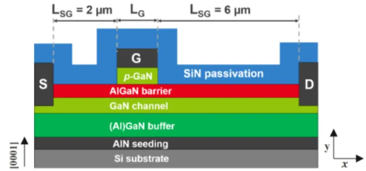
Fig. 1. Illustrative cross section plot (out of x-y scale) of the p-GaN gate HEMT considered in this study. Gate patterning and ohmic contact formation precede the SiN deposition.
II. STRUCTURE ANDSIMULATIONMETHODOLOGY
A. Device Structure
We consider the p-GaN gate HEMT structure shown in Figure 1 comprising a 2 µm (Al)GaN buffer, 30 nm GaN channel, 15 nm Al0.20Ga0.80N barrier and 100 nm p-type GaN
gate with 3 × 1017cm−3Mg acceptors density. TiN gate metal
thickness is 30 nm and SiN film thickness (tSiN) is set to
B. Simulation Methodology
A three-step simulation methodology shown in Figure 2 is employed to assess the impact of the stressed layer on the electrical characteristics of the p-GaN gate HEMT.
Fig. 2. Three-step simulation framework methodology used to predict the impact of the mechanical relaxation of the stressed passivation film on device characteristics.
1) Process Simulation: First, the mechanical state of the structure is determined by modeling device fabrication using Sentaurus Process 2D simulations [11]. The intrinsic stress of the passivation layer (σSiN) is varied from −2 GPa
com-pressive to +2 GPa tensile to reflect achievable experimental range [5]. A multi-layer deposition scheme consisting in 20 deposition steps is employed for accurate modeling of the mechanical impact of SiN film in the gate region [12].
2) Polarization Model: Then, the total polarization P in the III-N layers is calculated by summing the contributions of spontaneous and piezoelectric polarizations as P = Psp+Ppz.
Piezoelectric polarization is obtained from stress tensor σ and piezoelectric coefficients d as Ppz = d · σ in the
matrix-based formulation. Polarization-induced fixed charge density ρP arising from the spatial divergence of the polarization in
the III-N layers is calculated as ρP = −∇ · P
3) Device Simulation: Device simulations are performed using Sentaurus Device [13]. Fixed polarization-induced charge density is included in anisotropic Poisson equation and typical models used in the simulation of GaN-based HEMTs [14] as well as standard parameters for III-N materials [15] are employed.
III. RESULTS ANDDISCUSSION
A. Lateral Stress
The impact of the elastic stress relaxation of SiN on lateral stress (σxx) is depicted in Figure 3 for LG = 0.20 µm. For
unstrained SiN, the AlGaN layer is under constant tensile epitaxial stress and GaN layers are relaxed. However, non-uniform additional compressive (tensile) lateral stress is in-duced in the gate area in III-N layers due to compressive (tensile) built-in film stress and adds up to the initial stress. B. Polarization-Induced Charge Density
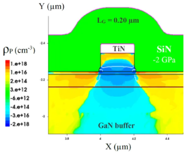
The distribution of polarization-induced charge density (ρP)
created in the gate region for LG = 0.2 µm is illustrated in
Figure 4. Fixed negative charges in the range 1016- 1018cm−3
are generated in the channel region and extend deeply in the GaN buffer. Moreover, SiN relaxation induces fixed positives charges to be created just outside the gate area.
Fig. 3. Vertical profile of lateral stress (σxx) along a cut performed at the
center of the gate. The mechanical interaction of the stressed layer in the gate vicinity leads to non-uniform σxxvariation along the c-axis direction.
Fig. 4. Two-dimensional distribution of the polarization-induced charge density (ρP) generated in the III-N heterostructure consequently of stressed
nitride layer deposition. σSiN= −2 GPa, LG= 0.2 µm.
C. Equilibrium Conduction Band Energy
The electrostatic charges generated in the III-N layers affect the conduction band energy (CBE) level in the channel region as shown in Figures 5 and 6. Compared to the reference structure (σSiN = 0 GPa), the CBE is significantly lifted
(lowered) by the effect of compressive (tensile) SiN stress. Results indicate that this shift of CBE is not limited to the p-GaN gate but extends deeper in the GaN buffer.
The horizontal profile of the CBE along the 2DEG region displayed in Figure 6 clearly shows tremendous modification of the gate depletion region due to SiN stress. Compressive (tensile) SiN leads to a higher (lower) and wider (narrower) gate depletion region. Furthermore, for a same stress magni-tude, σSiN > 0 leads to more significant changes of the CBE
profile and almost cancels the p-GaN gate induced potential barrier.
Fig. 5. Vertical profile of the equilibrium conduction band energy level (VGS= 0 V, VDS= 0 V), at the center of the gate, for varying σSiN.
Fig. 6. Horizontal profile of the equilibrium conduction band energy level (VGS= 0 V, VDS= 0 V) along the AlGaN/GaN interface for varying σSiN.
D. Device Transfer Characteristics
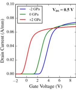
The simulated transfer characteristics of p-GaN gate HEMTs with LG = 0.2 µm for different values of σSiN are
shown in Figure 7. Consistently with the increased channel confinement discussed in Section III-C, the transfer character-istics exhibits a positive VTH shift when −2 GPa
compres-sively strained SiN is deposited on top of the p-GaN gate structure. Moreover, a slight increase in saturation current is observed. This is due to the positive polarization-induced charge density created outside the gate area.
Conversely, it is shown that the introduction of tensile SiN leads to a large negative threshold voltage shift such that the device is no longer normally-OFF. This is well explained by the critical degradation of the electron confinement observed in Figures 5 and 6. A slight decrease in saturation current
Fig. 7. Transfer characteristics IDS(VGS) of the simulated pGaN gate
HEMTs showing the impact of σSiN. The device embedding highly tensile
SiN film is no longer normally-OFF due to the large negative VTHshift.
is also observed due to negative polarization charge density created outsite the gate area.
E. Impact of Gate Length onVTH Shift
The gate length parameter plays a key role in quantifying the impact of SiN on device performances. Indeed, the interactions between the stress fields created in the III-N layers at both edges of the gate are magnified when the gate length is decreased. This is verified when plotting the evolution of the threshold voltage shift against intrinsic film stress in Fig-ure 8. When LGdecreases, the magnitude of ∆VTH increases
significantly. It is interesting to note that the trends are not symmetrical with respect to the sign of σSiN. Indeed, for
short gate lengths (LG < 0.5 µm), the magnitude of ∆VTH
is greater for tensile films than for compressive films. This is consistent with the evolution of the potential barrier observed in Section III-C. However this trend is reversed for longer gate lengths (LG ≥ 0.5 µm), where the magnitude of ∆VTH
is greater for σSiN < 0. This is due to the CBE increase at
both gate edges whereas for σSiN > 0, the CBE is lower at
gate edges but remains weakly impacted at gate center. F. Trade-off betweenVTH and RON
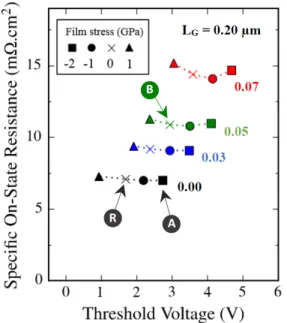
In order to evaluate more extensively the benefits of local stress engineering, simulations combining an AlGaN buffer (or back-barrier) and intrinsically stressed SiN were carried out. The Al content of the buffer (xbuffer) was changed from 0.00 to
0.07 and σSiN was ranged from -2 GPa to +1 GPa. Obtained
results are expressed in terms of the trade-off between the threshold voltage VTH and the specific on-state resistance
RON and displayed in Figure 9.
As compared to a reference GaN buffer device R with unstrained SiN (xbuffer = 0.00, σSiN = 0 GPa), devices with
Fig. 8. Threshold voltage shift versus σSiNfor varying LGvalues.
Fig. 9. Comparison of the trade-off between VTHand RONfor σSiNranging
from −2 GPa to 1 GPa and xbufferranging from 0.00 to 0.07.
RON increase, due to stronger confinement and partial
deple-tion of the 2DEG in the access region. Thus, while device B (xbuffer = 0.05, σSiN = 0 GPa) can increase VTH from 1.7 V
to 3.0 V, it also increases RON by ∼70%. On the other hand,
device A (xbuffer = 0.00, σSiN = −2 GPa) also increases VTH
of the reference device by nearly the same amount but without deteriorating RON. Therefore, local stress engineering of the
p-GaN gate HEMT can increase VTHalmost independently of
RON, which leads to a great improvement of the VTH-RON
trade-off. Moreover, this results clearly indicate that SiN stress effect can be incorporated in p-GaN gate HEMTs employing AlGaN back-barrier structures to achieve better performances.
In this way, the combination of both techniques could e.g. be used to increase the Al content of the AlGaN barrier to reduce RON while maintaining VTH around a value of 2 V.
IV. CONCLUSION
This paper reveals the crucial role of stress engineering in obtaining high-performance p-GaN gate normally-OFF HEMTs. While it is shown that tensile films deposited on top of the gate may lead to critical degradation of the safe operation, strategies employing compressively deposited thick films and relatively short gate lengths can be implemented to greatly improve the trade-off between the threshold voltage and the on-state resistance of the devices. Moreover, this technique can be used in conjunction with AlGaN back-barriers to furthermore increase the design margin.
REFERENCES
[1] O. Ambacher, B. Foutz, J. Smart, J. R. Shealy, N. G. Weimann, K. Chu, M. Murphy, A. J. Sierakowski, W. J. Schaff, L. F. Eastman, R. Dimitrov, A. Mitchell, and M. Stutzmann, “Two dimensional electron gases induced by spontaneous and piezoelectric polarization in undoped and doped AlGaN/GaN heterostructures,” Journal of Applied Physics, vol. 87, no. 1, pp. 334–344, Jan. 2000.
[2] W. Lu, V. Kumar, R. Schwindt, E. Piner, and I. Adesida, “A compara-tive study of surface passivation on AlGaN/GaN HEMTs,” Solid-State Electronics, vol. 46, no. 9, pp. 1441–1444, Sep. 2002.
[3] E. T. Yu and P. M. Asbeck, “Local Polarization Effects in Nitride Het-erostructures and Devices,” in Polarization Effects in Semiconductors, D. C. Wood and D. Jena, Eds. Springer US, 2008, pp. 217–264. [4] N. Shigekawa and S. Sugitani, “Numerical analysis of impact of stress
in passivation films on electrical properties in AlGaN/GaN heterostruc-tures,” IEICE Electronics Express, vol. 6, no. 14, pp. 1045–1050, 2009. [5] P. Morin, G. Raymond, D. Benoit, P. Maury, and R. Beneyton, “A comparison of the mechanical stability of silicon nitride films deposited with various techniques,” Applied surface science, vol. 260, pp. 69–72, 2012.
[6] H. Y. Wong, N. Braga, and R. Mickevicius, “AlGaN/GaN rake-gate HFET: A novel normally-off HFET based on stress and layout engineer-ing,” in Simulation of Semiconductor Processes and Devices (SISPAD), 2016 International Conference on. IEEE, 2016, pp. 61–64.
[7] W. Saito, Y. Takada, M. Kuraguchi, K. Tsuda, and I. Omura, “Recessed-gate structure approach toward normally off high-Voltage AlGaN/GaN HEMT for power electronics applications,” IEEE Transactions on Elec-tron Devices, vol. 53, no. 2, pp. 356–362, Feb. 2006.
[8] Y. Cai, Y. Zhou, K. Chen, and K. Lau, “High-performance enhancement-mode AlGaN/GaN HEMTs using fluoride-based plasma treatment,” IEEE Electron Device Letters, vol. 26, no. 7, pp. 435–437, Jul. 2005. [9] O. Hilt, A. Knauer, F. Brunner, E. Bahat-Treidel, and J. Wurfl,
“Normally-off AlGaN/GaN HFET with p-type Ga Gate and AlGaN buffer,” in 2010 22nd International Symposium on Power Semiconductor Devices IC’s (ISPSD), Jun. 2010, pp. 347–350.
[10] L. Lucci, J.-C. Barb´e, and M. Pala, “Full-quantum study of AlGaN/GaN HEMTs with InAlN back-barrier,” in Simulation of Semiconductor Processes and Devices (SISPAD), 2015 International Conference on. IEEE, 2015, pp. 128–131.
[11] Synopsys Inc., CA, USA, “Sentaurus Process User Guide,” 2015. [12] K. Loiko, V. Adams, D. Tekleab, B. Winstead, X.-Z. Bo, P. Grudowski,
S. Goktepeli, S. Filipiak, B. Goolsby, V. Kolagunta et al., “Multi-layer model for stressor film deposition,” in Simulation of Semiconductor Processes and Devices, 2006 International Conference on. IEEE, 2006, pp. 123–126.
[13] Synopsys Inc., CA, USA, “Sentaurus Device User Guide,” 2015. [14] S. Strauss, A. Erlebach, T. Cilento, D. Marcon, S. Stoffels, and
B. Bakeroot, “TCAD methodology for simulation of GaN-HEMT power devices,” in 2014 IEEE 26th International Symposium on Power Semi-conductor Devices IC’s (ISPSD), Jun. 2014, pp. 257–260.
[15] I. Vurgaftman and J. R. Meyer, “Band parameters for nitrogen-containing semiconductors,” Journal of Applied Physics, vol. 94, no. 6, p. 3675, 2003.