RESEARCH OUTPUTS / RÉSULTATS DE RECHERCHE
Author(s) - Auteur(s) :
Publication date - Date de publication :
Permanent link - Permalien :
Rights / License - Licence de droit d’auteur :
Bibliothèque Universitaire Moretus Plantin
Institutional Repository - Research Portal
Dépôt Institutionnel - Portail de la Recherche
researchportal.unamur.be
University of Namur
Unbalanced magnetron sputtered Si-Al coatings
Jacobs, Marco; Terwagne, Guy; Roquiny, Philippe; Bodart, Franz
Published in:
Surface and Coatings Technology
Publication date:
1999
Document Version
Publisher's PDF, also known as Version of record
Link to publication
Citation for pulished version (HARVARD):
Jacobs, M, Terwagne, G, Roquiny, P & Bodart, F 1999, 'Unbalanced magnetron sputtered Si-Al coatings: plasma conditions and film properties versus sample bias voltage', Surface and Coatings Technology, vol. 116-119, pp. 735-741.
General rights
Copyright and moral rights for the publications made accessible in the public portal are retained by the authors and/or other copyright owners and it is a condition of accessing publications that users recognise and abide by the legal requirements associated with these rights. • Users may download and print one copy of any publication from the public portal for the purpose of private study or research. • You may not further distribute the material or use it for any profit-making activity or commercial gain
• You may freely distribute the URL identifying the publication in the public portal ? Take down policy
If you believe that this document breaches copyright please contact us providing details, and we will remove access to the work immediately and investigate your claim.
silicon peak diffraction patterns indicates that all films containing both elements are composed of separated silicon and aluminium phases. The aluminium grains are bigger than the silicon ones and the dimension of the silicon grains decreases when the silicon concentration increases. When bias voltage is applied to the substrates, a contamination of argon is observed. On the contrary, no argon contamination is observed in pure aluminium films for all grounded coatings. The maximum argon concentration appears for bias voltages around−30 V and is proportional to the plasma ion density, which depends on the target composition. At lower bias voltages the argon concentration decreases and stays nearly constant below −60 V. The presence and the concentration of argon is correlated to heating of the substrate due to the impinging ions and electrons. © 1999 Elsevier Science S.A. All rights reserved.
Keywords: Coatings; Magnetron sputtering; PVD; Sialon; Si
xAly; Thin film
1. Introduction experimental conditions and the properties of thin Si– Al films produced by unbalanced DC magnetron, which will be used for further N+
2 and O+2 implantation in ‘Sialons’ are phases in the Si–Al–O–N and related
system based on the (Si,Al ) (O,N )
4tetrahedral structure. order to produce thin ‘Sialons’ coatings with specific properties [2]. Different sputtering Si
xAlytargets with a They have several interesting mechanical, chemical and
thermal properties to make them candidates for high composition varying from pure Al to pure Si were used. The composition, structure and deposition rates of the temperature applications. In past years, there has been
increasing interest in the deposition of composite films coatings produced by the different targets are discussed. We have also studied the composition, structure and to meet the scientific and technological requirements for
new and innovative coating properties. The aim is to temperature of the coatings when a negative bias voltage is applied to the sample holder.
combine the good properties of a relatively ductile or soft substrate, easy to produce, with relatively hard layers like hard ceramics to produce functional work pieces with optimal surface properties.
2. Experimental details
Preliminary study of the characterisation of unbal-anced magnetron sputtering Si–Al coatings has already
The coatings were deposited using an unbalanced DC been published [1]. In this work we have studied the
magnetron sputtering system placed in a small chamber of 0.05 m3 equipped with a 280 l/s turbomolecular pump
* Corresponding author. Tel.:+32-81-72-54-78;
which provides a base pressure of 10−7 Torr. A
sche-fax:+32-81-72-54-74.
E-mail address: [email protected] (G. Terwagne) matic view of the chamber is shown in Fig. 1(a). The
0257-8972/99/$ – see front matter © 1999 Elsevier Science S.A. All rights reserved. PII: S 0 2 5 7- 8 9 7 2 ( 9 9 ) 0 0 27 8 - 9
736 M. Jacobs et al. / Surface and Coatings Technology 116–119 (1999) 735–741
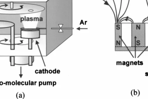
Fig. 1. (a) Schematic view of the unbalanced DC magnetron deposition chamber; (b) arrangement of the magnets in the cathode, the arrows indicate the field lines.
sputtering target consists of a 2-inch disk and is placed taking into account the relative area of Si and Al in the sputtered track, and also the sputtering yield of Si and just above the magnets with a good thermal contact in
order to cool the magnetic material with water during Al, which is respectively 0.5 and 1.05 for 500 eV argon ions [4]. Table 1 gives the expected composition and the deposition. The field lines of this unbalanced DC
magne-tron are shown in Fig. 1(b). The characteristic self-bias description of the sputtering targets used.
The Si–Al coatings were deposited on glassy carbon voltage for this configuration can vary from −25 V to
−33 V [3]. The sputtering target bias voltage was pro- at a pressure of 2.4 mTorr controlled by an argon mass flow meter. The magnetron power was set to 140 W duced by a 500 W DC power supply.
Six kinds of composite sputtering target were used in during deposition and the voltage applied to the sputter-ing target was around−500 V. Prior to deposition, each order to cover a wide range of concentrations of silicon
and aluminium for the samples. Pure aluminium ( T1) target was conditioned by sputtering for about 5 min with a shutter covering the source. The specimens were and silicon ( T2) disks were used to determine the
deposition rates of the pure elements. Moreover, two placed directly below the centre of the sputtering target, in line with the intense region of the plasma from the different Si–Al alloys were used: the composition of the
first target ( T3) provided by Pe´chiney ( Voreppe, France) unbalanced magnetron. The source to substrate distance was 70 mm. The deposition time was 5 min in order to is Si50Al50 and the second target (T4) provided by GfE
(Augsburg, Germany) is made from pressed powder of obtain a thickness of about 200 nm for the coatings. The substrate temperature was measured below 50°C aluminium and silicon with a composition of Si70Al30.
Targets T5 and T6 consist of home-made 2 in targets of during deposition with a thermocouple fixed at the rear of the substrate. A bias voltage can be applied to the aluminium with small disks of silicon placed where the
sputtering track is more important. The expected com- sample holder and the specimens were realised at different polarisation ranging from 0 V to −100 V. position for the home-made targets is calculated by
Table 1
Description of the sputtering targets used and calculation of the expected composition of Al and Si. The method used for determining the composition is explained in the text
Target number Expected composition Measured composition Thickness (1015 at/cm2) Description
T1 Al100 Al100 1700 Pure metallic aluminium T2 Si100 Si100 900 Silicon (111) (ACM, France)
T3 Si50Al50 Si38Al62 1380 Si–Al alloy (Pe´chiney, Voreppe, France)
T4 Si
70Al30 Si63Al37 1070 Pressed powder (GfE, Augsburg, Germany)
T5 Si
28Al72 Si29Al71 1290 Metallic aluminium with 2 disk of silicon (20 mm)
T6 Si
Fig. 2. Experimental ($) and simulated (—) RBS spectrum obtained with 2.0 MeV a-particles detected at 175° for a typical Si–Al coating deposited by unbalanced DC magnetron on a glassy carbon substrate.
3. Experimental results silicon contents by fitting the shoulder at the right of the Al–Si peak (expanded figure). The thicknesses of the Si–Al coatings are presented in Table 1. The depos-3.1. RBS measurements
ition rate for aluminium target is 5.6×10¹⁵ at cm−2 s−1 , which corresponds to 9.4 A˚ s−1 if we assume that the The thickness and composition of the coatings were
measured by Rutherford backscattering spectroscopy density of Al in the coating is 2.7 g cm−3. For the pure silicon target, the deposition rate is (RBS ) technique with 2 MeV incident a-particles. A
typical spectrum observed at a diffusion angle of 175° 3.0×10¹⁵ at cm−2 s−1 and corresponds to 6.0 A˚ s−1 if we assume that the density of Si in the coating is is shown in Fig. 2. The experimental data were simulated
using RUMP code [5] and the solid line represents the 2.3 g cm−3. We can observe that the deposition rate for aluminium is 1.9 times greater than the deposition rate simulated curve. The signals corresponding to Si and Al
cannot be resolved due to the fact that silicon and for silicon, which can be directly related to the ratio between sputtering yield of aluminium and silicon aluminium are too close, but it is possible to measure
738 M. Jacobs et al. / Surface and Coatings Technology 116–119 (1999) 735–741
Fig. 4. Experimental ($) and simulated (—) RBS spectrum obtained with 2.0 MeV a-particles detected at 175° for a Si–Al coating deposited on glassy carbon by unbalanced DC magnetron with the sputter target T4. The bias voltage of the sample holder was set to−32 V.
(1.05/0.5=2.1) [4]. For sputtering targets T3 and T4, a large difference between the expected composition and the measured composition can be observed, especially for the sputtering target T3. This disagreement can be explained by preferential sputtering of aluminium: when one atom of silicon is removed from the surface of the target, two atoms of aluminium are removed. The picture in Fig. 3 shows the sputter target T3 where the erosion is more important. We can observe in the sputtered track some dark lines, which have been corre-lated to silicon and big holes (metallic grey) where aluminium is located. Microanalysis by PIXE in the sputtered track has been performed and shows clearly that the target becomes poorer in aluminium at the surface when material is removed [6 ]. This effect can be explained by the difference in sputtering yield between aluminium and silicon.
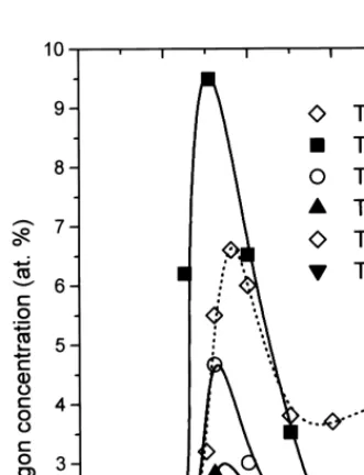
We have also studied the argon contamination versus bias voltage applied to the sample holder. Fig. 4 shows a typical RBS spectrum observed for the sputtering target T4 when the potential applied to the sample is −32 V. A huge contamination of argon appears in the whole Si–Al coating. The experimental data have been simulated using RUMP code [5] and the concentration of argon reaches 10 at% for the T4 sputter target
Fig. 5. Argon concentration obtained by RBS technique versus bias
(Fig. 5). When we plot the argon concentration versus
voltage of the sample holder.
the applied voltage of the sample, a narrow peak appears between−25 V and −40 V and the maximum
concen-tration of argon increases with silicon contents of the 3.2. XRD measurements sputtering target. Below−40 V, the argon concentration
decreases rapidly and remains constant for voltage lower Glancing angle X-ray diffraction (GXRD) was car-ried out using a Philips diffractometer with Co Ka than−60 V.
the bias voltage−80 V. RBS results indicate that the deposition rates depend on silicon contents of the sputter target. For bias voltage around the self-bias, a large contamination of argon 3.3. Temperature of the specimen
appears in the coatings (Fig. 5). A similar property has also been observed by Shedden et al. [7] for Al–Mg The temperature of the specimen during deposition
can be affected by the bias supply of the sample. In coatings. The authors explained that the coatings with order to study the influence of temperature, special
coatings were realised without cooling the substrate. We
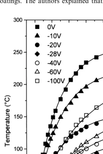
Fig. 7. Evolution of the substrate temperature versus deposition time Fig. 6. GXRD spectra observed for the sputter target T3 to T5. The for sample bias voltage ranging from 0 V to−100 V. The cathode
used for the deposition was T3. bias voltage of the sample holder was set to 0 V,−32 V and −80 V.
740 M. Jacobs et al. / Surface and Coatings Technology 116–119 (1999) 735–741
Fig. 8. Cross-sectional TEM pictures of the Si–Al coatings deposited with T4 cathode. The left picture (a) corresponds to a coating deposited with the self-bias voltage while the right one (b) was made with the sample holder connected to the earth.
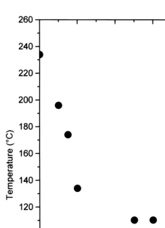
high argon content are formed by an amorphous phase, which crystallises after room temperature ageing. We have measured by cross-sectional TEM two different specimens. Fig. 8(a) is a TEM picture of a Si–Al coating made with a self-bias applied to the sample holder while Fig. 8(b) corresponds to the sample holder connected to the earth. Both coatings were made using sputter target T4. The large amount of argon appears when small columns [Fig. 8(a)] form the coating structure, while large grains of Si–Al appear when the sample is connected to the earth during deposition [Fig. 8(b)]. With the Thornton diagram [8], which shows the struc-ture of the coatings versus the temperastruc-ture of the specimen and the partial pressure of Ar, this property can be explained because large grains in the coating are observed when the temperature of the specimen increases. If we plot the temperature of the sample measured after 5 min versus bias voltage, we can observe a minimum temperature for a bias voltage around −30 V (Fig. 9). From 0 to −20 V, the voltage difference between the plasma and the sample holder is so small that electrons can reach very easily the specimen; the temperature of the specimen is only produced by electron impact and decreases very rapidly when the bias voltage decreases. For sample bias voltages between –20 V and – 40 V, Ar+ atoms are accelerated to the specimen and
Fig. 9. Evolution of the substrate temperature versus sample bias
volt-trapped into the coating because the temperature of the age. The data were recorded after 5 min of deposition and are related specimen is low. For smaller bias voltage (<−40 V ), to the measurements presented in Fig. 7.
the temperature of the specimen increases due to ionic implantation of Ar but electrons cannot reach the
sur-face. When the temperature of the specimen increases, the width of the peak due to aluminium at 45° decreases with the bias voltage of the sample holder, which means the size of the grains in the coating increases also, and
less argon can be trapped into the layer. XRD measure- that crystalline Si–Al coatings are formed when the bias voltage of the specimen is lower than –40 V. An impor-ments confirm this property. For samples T3 and T5,
Argon contamination in the coatings depends [5] L.R. Doolittle, Nucl. Instrum. Meth. B 9 (1985) 344.
[6 ] G. Terwagne, F. Bodart, Proceedings of the 6th International
Con-strongly on the bias voltage applied to the substrate
ference on Nuclear Microprobe Technology and Applications,
holder. A maximum concentration of argon and smaller
Spier Estate, South Africa, 1998.
size grains growing in a columnar structure are observed
[7] B.A. Shedden, M. Samandi, B. Window, Surf. Coat. Technol. 97
when the bias voltage is around the self-bias. The lower (1997) 557.
temperature of the substrate explains this effect when [8] Y. Pauleau, Materials and Processes for Surface and Interface Engi-neering, Kluwer Academic, Dordrecht, 1997.