HAL Id: tel-01083881
https://tel.archives-ouvertes.fr/tel-01083881
Submitted on 18 Nov 2014
HAL is a multi-disciplinary open access archive for the deposit and dissemination of sci-entific research documents, whether they are pub-lished or not. The documents may come from teaching and research institutions in France or abroad, or from public or private research centers.
L’archive ouverte pluridisciplinaire HAL, est destinée au dépôt et à la diffusion de documents scientifiques de niveau recherche, publiés ou non, émanant des établissements d’enseignement et de recherche français ou étrangers, des laboratoires publics ou privés.
materials on InP for optical telecommunication
Yu Zhao
To cite this version:
Yu Zhao. Growth and optical characterization of Sb-based materials on InP for optical telecommuni-cation. Optics / Photonic. INSA de Rennes, 2014. English. �NNT : 2014ISAR0002�. �tel-01083881�
Growth and
optical characterization of
Sb-based materials on InP
for optical
telecommunication
Thèse soutenue le 11.02.2014
devant le jury composé de :
Éric Tournié
Professeur - Université de Montpellier 2 / rapporteur / président du jury
Régis André
Directeur de recherche - Institut Néel Grenoble / rapporteur
François Julien
Directeur de recherche - IEF Orsay / examinateur
Paul Koenraad
Professor - Technische Universiteit Eindhoven / examinateur
Anne Ponchet
Directeur de recherche - CEMES Toulouse / examinateur
Hervé Folliot
Professeur - INSA de Rennes / Co-encadrant de thèse
Mathieu Perrin
Maître de conférences - INSA de Rennes / Co-encadrant de thèse
THESE INSA Rennes
sous le sceau de l’Université européenne de Bretagne pour obtenir le titre de DOCTEUR DE L’INSA DE RENNES Spécialité : Physique-Optoélectronique
présentée par
Yu ZHAO
ECOLE DOCTORALE : SDLM
Growth and optical characterization of
Sb-based materials on InP for
optical telecommunication
Remerciement
Les études présentées dans cette thèse ont été réalisées pendant une durée de trois ans dans le laboratoire FOTON-OHM à Rennes.
Je tiens dans un premier temps à remercier Nicolas Bertru, Hervé Folliot et Mathieu Perrin, pour avoir m’avoir confié ce travail de recherches et m’avoir encadré quotidien-nement. Leurs grandes expériences dans l’épitaxie et dans les caractérisations optiques m’ont toujours éclairé. Mes remerciements vont aussi à Antoine Létoublon, pour ses expertises de diffraction de rayon X.
Durant ces trois années, j’ai pu vivre dans un milieu particulièrement agréable et ces travails n’auraient pas pu aboutir sans l’aide de l’ensemble des membres de l’équipe : Tony Rohel pour la croissance SSMBE et Marianne Prévôt pour la première version de banc d’absorption …
Cette thèse ne serait pas complète sans des nombreuses collaborations à l’extérieur du laboratoire. Je tiens mes remerciements particulièrement à Anne Ponchet et Julien Nicolaï pour les analyses TEM et pour m’avoir accueilli dans leur laboratoire. J’adresse un grand remerciement aussi à Professeur Paul Koenraad et Samuel Mauger de Tech-nische Universiteit Eindhoven pour leurs excellentes analyses X-STM. Nous remercions aussi François Julien pour nous avoir permis à réaliser les premiers mesures d’absorp-tion inter-sous-bandes dans son laboratoire. Je voudrais également exprimer toute ma reconnaissance à M. Régis Andrés et M. Éric Tournié, qui m’ont fait honneur d’avoir rapporté cette thèse et d’avoir participé au jury de soutenance.
Ces remerciements ne seraient pas complets sans une pensée pour les « jeunes » du laboratoire et des amis que j’ai eu le plaisir de côtoyer durant ces quelques années à Rennes.
Mes dernières pensées iront vers mes parents, qui m’auront permis de poursuivre mes études jusqu’à aujourd’hui.
Contents
Introduction 1
1 Epitaxial Growth of Antimonides on InP Substrate 7
1.1 MBE system . . . 8 1.2 Epitaxial growth of lattice-matched alloys on InP substrate . . . 9 1.3 Deposition of lattice-mismatched materials on InP substrate . . . 11 2 The Growth of Ga0.47In0.53As/AlAs0.56Sb0.44 Quantum Wells for
Inter-subband Applications 17
2.1 Inter-subband transition and devices . . . 18 2.2 Inter-band properties of GaInAs/AlAsSb multiple quantum wells . . . 22 2.3 Inter-subband properties of GaInAs/AlAsSb multiple quantum wells . . . 26 2.4 The effects of surface terminations . . . 35 2.5 The impact of digital alloy growth . . . 43 3 Sb-mediated Growth of InAs/AlAs0.56Sb0.44 Strained Quantum Wells
for Inter-subband Applications 53
3.1 Properties of InAs/AlAsSb strained quantum well . . . 54 3.2 Sb-mediated Growth of InAs on InP substrate . . . 55 3.3 Sb-mediated growth of pseudomorphic InAs/AlAsSb single quantum well 58 3.4 Strain compensation in InAs/AlAsSb multiple quantum wells . . . 64 3.5 Polarization-dependent absorption in InAs/AlAs0.56Sb0.44multiple
quan-tum wells . . . 68 4 Sb-mediated Growth of InAs/GaAs0.51Sb0.49 Heterostructures on InP
Substrate 75
4.1 InAs quantum dots on grown on (001) and (113)B substrates . . . 76 4.2 InAs/GaAs0.51Sb0.49quantum wells on InP (001) substrate . . . 79 4.3 Surface-orientation dependent surfactant effect of Sb . . . 91 5 Incorporation of Sb in Strained InAs(Sb) Heterostructures 97
5.2 Sb-incorporation in InAs/Al0.48In0.52As quantum wells . . . 101
Conclusion 107 Résumé 109 Appendices 119 A.1 Inter-subband absorption workbench . . . 119
A.2 Thermodynamic calculations on the composition of InAs1−xSbx . . . 120
A.3 Surfactant effect on the surface of Ga0.47In0.53As . . . 125
Introduction
Silica optical fiber networks are nowadays deployed all over the world and they connect the continents by transmitting infrared light signals in 1.55 µm band. InP-based lasers and photo-detectors are deployed to generate and to pick up light-signal transmitted in long-haul telecommunication networks. The telecommunication infrastructure has never stopped evolving, to meet the ever-increasing demand of Internet traffic. Many InP-based devices are being researched on to enable even faster modulation, denser multiplexing and more sophisticated modulation scheme. For example, InP-based light source like InAs/InP quantum-dash lasers is able to generate clock signal at a repetition rate over 300 GHz [1]. On the electronic side, InP-based GaInAs transistor can operate at frequencies as high as 710 GHz [2] and it can be easily integrated with current InP-based technologies.
Paradoxically, advanced signal processing in optical networks relies on electronics. Various conversions between light and electronic signals are performed during the journey of each bit of information and the limit of electronics will one day be a bottleneck to achieving faster data exchange. At the same time, scaling up such electronics-based infrastructure will lead to elevated energy cost [3].
To overcome such limits, full-optical signal processing has been proposed to by-pass the electronics. The modulation of light signal boils down to rapid change of optical functions of the transmitting medium. Inter-subband transition in a quantum-well structure is one of the physical processes that enable fast attenuation and refractive index change. It enables fast switching from ON-state to OFF-state in a fraction of one pico-second [4,5], which corresponds to a modulation rate even higher than 1 THz. Besides the fastness, its high non-linear properties [6] also mark potential uses in efficient modulation schemes like high-order phase-keying. Many quantum-well structures that allow inter-subband transition at 1.55 µm have been studied for potential use in full-optical signal processing, ranging from GaN/AlGaN [7], ZnSe/CdSe [8], to GaInAs/-AlAsSb [5] quantum wells which is fully compatible with InP substrate.
Many of the aforementioned structures are developed using epitaxy technologies like molecular beam epitaxy (MBE). For it can achieve sharp interface and thickness preci-sion down to one atomic layer, this thin film growth technology is able to realize many nanostructures as-designed. Also, its various adjustable growth parameters are
indis-3.0 2.5 2.0 1.5 1.0 0.5 0.0 5.4 5.6 5.8 6.0 6.2 6.4 6.6 W ave le ngt h ( µm ) 10 5 2 1 0.5 Lattice Constant (Å) B and ga p (e V) AlSb GaSb InSb InAs GaP AlP AlAs InP GaAs AlAs0.56Sb0.44 Ga0.47In0.53As GaAs0.51Sb0.49 Γ Valley X Valley
0 K
Figure 1: Band-gaps and lattice constants of common III-V compound semiconductor
com-pounds and their alloys (0 K). Direct band-gap alloys are interpolated by solid curves while indirect ones are dot or dashed lines. Reproduced according to [9].
pensable for structure optimization. Furthermore, various analyzing facilities integrated in MBE growth chamber enable in situ observation of epitaxial growth mechanism. MBE is hence the choice for the research of less adopted materials like antimonide alloys.
Figure 1 illustrates band gap and lattice parameters of commonly used III-V semi-conductors. Antimonide compounds like GaSb and InSb have smaller band gaps than most common III-V semiconductors, and they are found in lower part of figure1. They are found very useful in mid-infrared light generation and detection. However, it is diffi-cult to integrate these compounds in InP-based devices for their large lattice constants. Fortunately, by alloying antimonides with arsenic compounds, they can form ternary alloys like AlAs0.56Sb0.44and GaAs0.51Sb0.49 that are lattice-matched to InP substrate. The incorporation of Sb in these alloys leads to smaller band-gap as compared to their arsenic components. At the same time, they introduce new band line-up with mate-rials that is commonly used on InP substrate like GaInAs. Together, they offer new possibilities in InP-based applications.
Figure 2 shows several semiconductor alloys that are lattice-matched to InP sub-strate. GaInAs/GaAsSb quantum wells possess a type-II line-up with an effective gap as small as 0.3 eV. This makes it suitable for infrared generation and detection in 3-5 µm band. On the other side of the spectrum, (Ga)InAs/AlAsSb quantum wells has a conduction band offset as large as 1.6 eV [9]. Such deep electron confinement potential profile allows inter-subband transition in mid-infrared and even near-infrared range. For one thing, it allows quantum cascade laser operating at 3 µm. For another, it enables inter-subband absorption near 1.55 3 µm(0.8 eV) that find its uses in full-optical signal processing. Realizing inter-subband transition at 3 µm with these material is a major
-1.5 -1 -0.5 0 0.5 1 1.5 2 Ene rgy (e V) Materials ECΓ EVA 300 K 0.41 0.52 0.14 1.74 0.64 -0.94 -0.20 -0.60 -0.64 -0.72 InP GaAs0.51Sb0.49 Ga0.47In0.53As AlAs0.56Sb0.44 (indirect) Al0.48In0.52As
Figure 2: Band line up of several ternary alloys that are lattice matched to InP. Data are taken
from [9].
topic studied in this thesis.
Beside antimonide alloys, elemental Sb has also found important uses in the epitaxial growth of lattice-mismatched materials. Usually, by depositing an epitaxial materials that have much larger lattice constants than that of substrate, the deposit would organize into quantum dots structures (three-dimensional nanometric islands). The use of Sb in such growth can significantly increase the quality of the epitaxial thin film; and yet Sb atoms incorporate little and mostly stay on the growth surface [10]. It was demonstrated that the use of Sb can effectively delay the formation of quantum dots or the generation of dislocations [11, 12]. This aspect of Sb is known as surfactant effect for it being a surface active agent. Under other circumstances, the use of Sb has also demonstrated enhancement to the properties of quantum-dot structures, including increased island density, more uniform size distribution , as well as several other benefits [13–15]. Although these Sb-related phenomena have important technological uses in device elaboration, their mechanisms are often disputed.
The use of antimonides and surfactant effect of Sb being the clue of this thesis, it is developed as follows:
• Chapter 1 will provide more details on MBE growth, especially the growth of antimonide alloys on InP substrate. Following that, different epitaxial growth modes of lattice-mismatched materials are introduced .
• Chapter 2 begins by attempting to tune inter-subband absorption wavelength of Ga0.47In0.53As/AlAs0.56Sb0.44 quantum well structures to 1.55 µm, which is how-ever not achieved. A series of growth optimization and microscopic study were con-ducted, and these results indicate that multiple imperfections within such
struc-tures, such as the unintended incorporation of Sb into GaInAs layer, could be responsible.
• Chapter 3 advances the findings of chapter 2 and tries to shorten inter-subband transition wavelength, by replacing lattice matched Ga0.47In0.53As/AlAs0.56Sb0.44 with strained InAs/AlAs0.56Sb0.44. At a first time, the surfactant effect of Sb has well exercised its power and ensures good quality of single quantum well. Following that, stacking of these quantum wells were obtained by means of “strain compen-sation”. At the end of this chapter, preliminary investigation into inter-subband transition in strained InAs/AlAs0.56Sb0.44 quantum wells will be presented. • Chapter4explorers the influence of Sb on the InAs deposition on different substrate
orientations, in order to better understand the surfactant effect of Sb . Completely different growth behaviors were observed for InAs deposition on (001) and (113)B surfaces of GaAs0.51Sb0.49. The spectacular differences are interpreted by surface orientation dependent surfactant effect of Sb.
• Chapter 5 closes this thesis with preliminary investigations on the incorporation of Sb in highly-strained InAs layer on InP substrate. The use of Sb during the deposition of InAs(Sb) introduces two competing effects: it helps maintain layer-by-layer growth by covering the surface; at the same time, it favors the formation of relaxed island for it contributes more strain energy by incorporating into InAs. The practice of such growth could serve as a test of the effectiveness of Sb surfactant effect, and at the same time it can gives some reflections on the magnitude of competing energetic terms.
References
[1] K. Merghem et al., “Pulse generation at 346 GHz using a passively mode locked
quantum-dash-based laser at 1.55 m”,Applied Physics Letters 94, 021107 (2009).
[2] W. Hafez et al., “12.5 nm base pseudomorphic heterojunction bipolar transistors achieving f_T=710
GHz and f_max=340 GHz”,Applied Physics Letters 87, 252109 (2005).
[3] O. Wada, “Recent progress in semiconductor-based photonic signal-processing devices”, IEEE
Journal of Selected Topics in Quantum Electronics 17, 309–319 (2011).
[4] J. Hamazaki et al., “Ultrafast intersubband relaxation and nonlinear susceptibility at 1.55 m in
GaN/AlN multiple-quantum wells”,Applied Physics Letters 84, 1102 (2004).
[5] T. Akiyama et al., “1.55 m picosecond all-optical switching by using intersubband absorption in
InGaAs-AlAs-AlAsSb coupled quantum wells”,IEEE Photonics Technology Letters 14, 495–497
(2002).
[6] S.-i. Gozu et al., “Cross phase modulation efficiency enhancement in in0.8 Ga0.2As / Al0.5Ga0.5As / AlAs0.56Sb0.44 coupled double quantum wells by tailoring interband transition wavelength”,
Applied Physics Express 2, 042201 (2009).
[7] M. Tchernycheva et al., “Systematic experimental and theoretical investigation of intersubband
[8] R. Akimoto et al., “Ultrafast intersubband optical switching in II-VI-based quantum well for optical
fiber communications”,physica status solidi (b) 243, 805–812 (2006).
[9] I. Vurgaftman et al., “Band parameters for III–V compound semiconductors and their alloys”,
Journal of Applied Physics 89, 5815 (2001).
[10] T. F. Kuech, “Surfactants in semiconductor epitaxy”, in AIP conference proceedings, Vol. 916
(2007), p. 288.
[11] J. C. Harmand et al., “GaInAs/GaAs quantum-well growth assisted by sb surfactant: toward 1.3 m
emission”,Applied Physics Letters 84, 3981–3983 (2004).
[12] C. Gatel et al., “Analysis by high-resolution electron microscopy of elastic strain in thick InAs
layers embedded in Ga0.47In0.53As buffers on InP(0 0 1) substrate”,Acta Materialia 58, 3238–
3246 (2010).
[13] N. Kakuda et al., “Sb-mediated growth of high-density InAs quantum dots and GaAsSb embedding
growth by MBE”,Applied Surface Science 254, 8050–8053 (2008).
[14] A. Gocalinska et al., “Suppression of threading defects formation during sb-assisted metamorphic
buffer growth in InAs/InGaAs/InP structure”,Applied Physics Letters 100, 152112 (2012).
[15] W. LU, “Elaboration par épitaxie par jets moléculaires et caractérisation de nanostructures à base d’antimoine sur substrats InP”, PhD thesis (Institut National des Sciences Appliquées de Rennes, Rennes, France, 2010), 214 pp.
Epitaxial Growth of Antimonides
on InP Substrate
This chapter is dedicated to introducing all the epitaxially grown materi-als studied in this thesis. At a first time, the solid source molecular beam epi-taxy (MBE) system along with its major growth parameters are shortly cov-ered in section1.1. Following that, section1.2 explains how lattice-matched materials like Ga0.47In0.53As and AlAs0.56Sb0.44 are elaborated on InP sub-strate, and the choice of their growth conditions. These ternary alloys are essential to inter-subband applications studied in chapter 2 and 3. The fi-nal section 1.3 walks through different manner in which the deposition of lattice-mismatched material like InAs could would behave on InP substrate. According to deliberately manipulated growth conditions, different degrees of strain relaxation could result in either fully-strained two-dimensional InAs layer or three-dimensional InAs quantum dots, which are essential to the subjects studied in subsequent chapters3-5.
1.1 MBE system
All the samples studied in this thesis were prepared using a Riber 21T compact solid-source MBE system. Figure 1.1 illustrates its growth chamber, an ultra-high vacuum (UHV) enclosing where the epitaxial growth takes place. In essential, it consists of a set of evaporation cell sending molecular beams to a heated substrate. Therefore, they define the most important growth parameters of MBE growth: substrate temperature and flux intensities (pressures) of molecular beams.
Substrate for crystal growth is mounted onto molybdenum holders, which is heated from its back side during the growth. The heater reading number is measured by thermo-sensor, which is calibrated by well-known temperatures, like surface reconstruc-tion transireconstruc-tion temperature and melting points. The substrate temperature is stabilized by partial-integral-differential controllers to ensure fluctuation smaller than 0.1 °C . The eventual run-to-run temperature difference is estimated to be less than 5 °C.
Sif/fBe dopants substratef shutter heater Pf/fAsf/fSb valvedfcrackerfcell Nf RFfplasmafcell heatingfwire Alf/fGaf/fIn effusionfcell
Figure 1.1: An illustrative representation of MBE growth chamber (Riber 21T)
The molecular beam fluxes are produced by different type of source cells. Group-III elements like Al, Ga, In as well as doping atoms like Si and Be are evaporated using Knudsen-type effusion cells. In these type of cell, molecular beams are produced by heating substances contained in ceramic crucibles. A mechanic shutter plates is installed in front of each cell to enable on-off flux modulation. Since flux intensities of these elements are solely determined by the cell temperature, they cannot be changed rapidly. In order to realize rapid change of a given elemental flux within one growth-run, redundant cells should be equipped. Group-V elements like P, As, Sb are produced by more sophisticated valved-cracker cell. In these cells, the micrometric valves enable rapid flux variation. Also, pure solid are not only evaporated but also pyrolyzed at a high-temperature cracking stage, turning Sb4into Sb2for example. The use of bi-atomic molecules like Sb2 can significantly modifies the incorporation behavior of Sb, and this will be further addressed in chapter 5.
The output of each source cell is measured by a retractable flux gauge positioned in front of the substrate. The gauge readings are recorded in beam equivalent pressure ; they are actively monitored before each growth-run and consistent output of each cell is crucial for reproducible results. Tn the literatures beam equivalent pressures are commonly given to describe growth conditions, but in practice growth parameters like growth-rate are equally important. This will be explained shortly.
1.2 Epitaxial growth of lattice-matched alloys on InP
sub-strate
Figure 1.2offers a microscopic view of substrate surface under MBE growth. At a first time, the incoming molecules or atoms get adsorbed on the surface and then get involved in a series of surface processes like massive migration across all kinds of features on the growth surface (surface diffusion). Eventually, the ad-atoms could settle down and join the lattice, or possibly gain enough energy and leave the growth system (desorption). Many of these processes can be kinetically controlled, which makes MBE growth de-pendent of substrate temperature and other specific growth parameters in a complex manner.
nucleation
surface diffusion
desorption
adsorption molecular / atomic beam
Figure 1.2: MBE growth surface
During the growth of binary compound like GaAs, over-saturated level of group-V element (As) is usually supplied, that is, under a V/III beam equivalent pressure ratio greater than 1. Under such circumstances, the desorption of group-III element (Ga) is negligible and they have unity sticking coefficient. On the other side, the desorption of group-V atoms (As) is significant and it has complex dependence on growth parameters. In practice, growth rate is used to describe the incorporating rate of group-III element. It is determined by thickness of materials grown in given time and it is usually expressed in mono-layer per second (ML/s). Experimentally, the growth rate is measured with the help of strained super-lattice composed of repeated InP/AlInP pairs of thick InP and very thin AlInP layers for example. The thickness of GaAs layers can be approximated
by the thickness of one super-lattice period, which is in turn measured by ω-2θ scans in X-ray diffraction.
The growth of ternary alloys like Ga0.47In0.53As and Al0.48In0.52As is simply done by co-deposition of their constituent binary alloys GaAs, AlAs and InAs. For alloys like GaInAs, which contains two types of cations (group-III elements) and one anion, its composition can be well estimated by the growth rates of cations since cation desorption is usually negligible. For example, the growth Ga0.47In0.53As is achieved by simultaneous deposition of Ga and In, at growth rates of 0.11 ML/s and 0.12 ML/s respectively.
For the growth ternary alloys like AlAs0.56Sb0.44 or GaAs0.51Sb0.49, which contain different anions (group-V elements), the achievement of lattice-matching condition is more challenging. Due to the desorption of anions, the alloy composition is influenced by the substrate temperature and even the growth rate of cation (group-III element) [1, 2]. Nevertheless, the desorption of anion can be reduced by sending equal amount of anion and cation to growth surface. In practice, this corresponds to a low V/III beam equivalent pressure ratio, and the desired AlAsSb composition can be found by varying the growth rate of Al while keeping group-V flux at constant level. The composition of such alloys is routinely checked, and the misfit of AlAs0.56Sb0.44 and GaAs0.51Sb0.49 grown on InP substrate are kept lower than 0.1% (AlAsSb 0.07%, GaAsSb 0.05%).
Unlike Ga0.47In0.53As, a classical material for InP substrate, much less information is available about the growth of AlAs0.56Sb0.44 lattice-matched to InP substrate [1–7] or about its optical properties [8–10]. Quaternary AlGaAsSb has been employed used in integrated Bragg mirror for its low refractive index [2, 11] , while GaInAs/AlAsSb are used in quantum cascade lasers [12–14] and inter-subband transition optical switch for its high conduction band offset. Among these applications, a wide range of growth temperatures have been reported from 540 °C [3] to as low as 400 °C[7], although mis-cibility gap is predicted in a wide range of composition [15]. Actually, clusters of AlAs were observed [5] in AlAsSb alloy grown under low growth rate and low temperature, and these defects can be eliminated by raising growth temperature to above 500 °C. Such elevated temperature poses yet another problem for the growth of Ga0.47In0.53As : desorption of indium becomes significant at such elevated temperature. As the first step towards InP-based inter-subband transition application, (Ga)InAs/AlAs0.56Sb0.44 structures presented in this thesis were all prepared at 450 °C, which is adapted to the elaboration of other InP-based structures. We leave temperature optimization for future studies.
Another issue concerning the growth of AlAsSb is the segregating nature of antimony. Compared to arsenic, antimony has lower binding energy with cations. The first layers of AlAsSb could be As-rich due to the segregation of Sb. In addition, Sb also has much lower saturating pressure which allows it cumulates on growth surface rather than evaporates into gas phase. This portion of segregated Sb could be incorporated into
subsequent layers and smear the interface between antimonide and antimony-free layers. Special surface termination method can be employed to counteract the segregation of Sb. For example, long-time growth interruption under As2-flux can purge accumulated surface Sb [16].
The aforementioned growth conditions described how alloys like Ga0.47In0.53As, Al-As0.56Sb0.44, Al0.48In0.52As and GaAs0.51Sb0.49can be grown individually; however, they cannot be grown within the same growth-run, since no set of constant flux can accom-modate the growth of these four alloys. This is currently solved by using redundant gallium and indium source-cells.
1.3 Deposition of lattice-mismatched materials on InP
sub-strate
Growth modes of heteroepitaxy
The epitaxial growth of heterostructure may proceed under three distinct growth modes: the Frank van der Merwe mode for two-dimensional layer-by-layer growth, the Stranski--Krastanow mode for layer-plus-island growth, and Volmer-Webber mode for three-dimensional direct island formation; they are illustrated in figure1.3. The growth mode of a given material system is largely determined by strain energy stocked in the epi-taxial thin film(ε2D
strain), the surface energies (γ2, γ3, γ4) and interface energy at the substrate-epitaxial thin film interface (γ1).
For the growth of aforementioned lattice-matched materials like Ga0.47In0.53As, its growth mode is solely determined by the interface and surfaces energies. Layer-by-layer growth mode usually occurs if the surface and interface energies introduced by epitaxial layer is lower than the surface energy of matrix ( γ2 + γ1 < γ3 in figure 1.3). The epitaxial layer is considered to be wetting the matrix. Otherwise, the epitaxial growth will proceed under Volmer-Webber growth mode and non-wetting islands are formed.
The growth of lattice-mismatched material is more complicated for it involves strain energy and subsequently strain relaxation. The epitaxial layer may either maintain full coherence with the substrate, form three-dimensional islands that enable partial strain relaxation, or release strain energy by generating defects.
In case of high lattice-mismatch, the strain energy is so dominant that no other energy term can compete with it (E2D
strain≫ Estrain3D ). The epitaxial grown material could directly organize into islands under Volmer-Webber mode.
When the lattice mismatch is intermediate, the system can go under Stranski--Krastanow growth mode : the epitaxial growth maintains two-dimensional wetting-layer until a critical thickness is reached. The system then switches to three-dimensional mode, forming islands upon the wetting layer. The critical thickness for
γ1 γ4 γ3 ε2D ε3D Stranski-Krastanow Volmer-Weber matrix γ2 ε2D
Frank-van der Merwe
ε3D
matrix
Figure 1.3: Three growth modes of heteroepitaxy : Frank-van der Merwe, Volmer-Webber, and
Stranski-Krastanow.
example, a critical thickness of 1.5–1.8 mono-layer (ML) is determined for InAs deposi-tion on GaAs under a wide range of growth condideposi-tions, and a wetting layer of similar thickness can still be observed by ex situ observations like cross-sectional scanning tun-neling microscope [17]. Stranski-Krastanow growth mode is crucial to self-assembled InAs quantum dots, for they can produce coherently strain islands that powers devices like quantum-dot lasers.
Strain relaxation
Coherently strained layer or coherent islands can exist during the initial stage of de-position; however, their growth cannot proceed without limit. The lattice strain will cumulate until a critical thickness, beyond which strain energy would be released via elastic relaxation by generating undulation, or via plastic relaxation by generating dis-locations and other defects. These different ways of strain relaxation are illustrated in figure1.4. Neither of these relaxation is desired, since they degrade electronic properties and device performance.
Figure 1.4: Coherent epitaxial layer, elastic relaxation and plastic relaxation
its lattice constants. As is demonstrated in figure 1.4, fully coherent epitaxial layer is subject to elastically tetraorthogonal deformation. Its in-plane lattice constant a is deformed to match that of substrate asub, while its vertical lattice constant a⊥ can be estimated by :
a⊥= a0− 2ν
1 − ν(asub− a0) (1.1)
in which a0 is relaxed lattice constant of epitaxial material, and ν represents its Poisson’s ratio. The vertical lattice constant a⊥ can be easily determined by X-ray diffraction measurements, and deviation from the value predicted in equation (1.1) signifies strain relaxation.
The critical thickness for plastic relaxation hc can be estimated by calculations prior
to actual growth. Matthews and Blakeslee [18] proposed a criterion for plastic relaxation based on the movement of dislocations, which can often give an idea about the limit of pseudomorphic growth regime [19]1:
hc = |b| 2 · 4 · πf 1 − ν cos2θ (1 + ν) cos λln (h c |b|+ 1 ) (1.2)
a is the lattice constant of substrate, f = (asub− a0)/a0 is the misfit between epitaxial material and substrate, and ν is the Poisson’s ratio of epitaxial layers. If we choose the most prevalent 60° dislocation in zinc-blende structure, its Burgers vector |b| =
a[1 0 1]/2 = √
2a0/2, and direction cosines cos θ = cos λ = 1/2. Poisson ratio ν is taken as 1/3, a good approximation for many compound semiconductor materials. Compared to the original expression of Matthews-Blakeslee, the first factor of equation (1.2) has an extra denominator 4. It counts for the fact that epitaxial thin film is constraint only from one side [19]. Equation (1.2) is solved over a wide range of misfit and corresponding solutions are shown in figure 1.5.
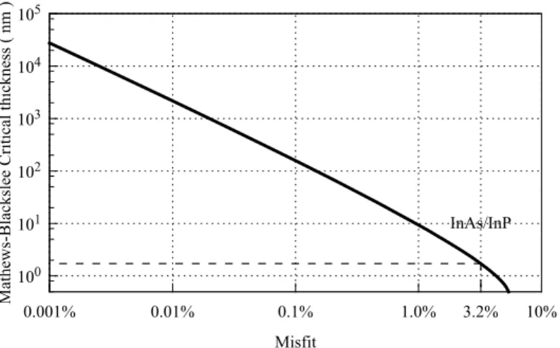
The lattice constant of InAs is 3.2% larger than that of InP, and its critical thickness for plastic relaxation is only about 1.7 nm (∼3 ML) by the criterion of Matthews-Blakeslee. Due to its band-gap as low as 0.4 eV, strained InAs quantum wells on InP substrate can potentially extend the working wavelength of InP-based device to mid-infrared range. In reality, InAs deposition on InP goes under Stransky-Krastanov growth mode upon 1–2 ML (0.3–0.6 nm) deposition, which limits its emission wavelength below 2µm.
Surfactant effect and Sb
The growth mode of InAs can be significantly modified by the deliberate introduction of surfactant atoms like Sb. The use of Sb is known to help maintain two-dimensional growth mode of lattice-mismatched epitaxial layers [20,21]. By applying Sb flux during
1This critical thickness for plastic relaxation is different from critical thickness for growth-mode
100 101 102 103 104 105 0.001% 0.01% 0.1% 1.0% 3.2% 10% Ma the ws-B la cksl ee C rit ic al thi ckne ss ( nm ) Misfit InAs/InP
Figure 1.5: Critical thickness for plastic relaxation obtained by Matthews-Blackslee formula
1.2
their deposition, thick and yet defect free InAs layer of high quality was obtained on InP substrate, and yet the incorporation level of Sb was negligible [21]. The use of surfactant was taken as surface energy modifications, which increase energy barrier for strain relaxation [22]. The use of surfactant was also considered to shift the balance between competition between elastic and plastic relaxation [22] and subsequently critical thickness for dislocation generation as well as critical thickness for elastic relaxation [20]. We attempt to achieve 1.55 µm inter-subband transition within strained InAs/AlAs0.56 -Sb0.44 quantum wells. The limit of such Sb-assisted growth as well as its relaxation behavior is studied in chapter3.
The effect of surfactant is also taken as modification of surface diffusivity of Indium atom, and a surfactant atoms can enhance or reduced diffusion length of cation ad-atom [23]. In these scenario, the surfactant effect of Sb is attributed to its complete surface coverage: arriving ad-atoms are instantly swapped with sub-surface Sb atoms and by consequence their surface mobility is significantly reduced. [20,24]. Such kinetic diffusion blocking has also been employed to explain high density and uniform quantum dot that were obtained under the influence Sb [25].
It has been demonstrated that the use of surfactant can modify the equilibrium shape of strained Ge/Si deposition, and degree of energy modification is considered facet orientation dependent [26]. In chapter 4, the effect of Sb on the deposition of strained InAs is again examined on both (001) and (113)B surfaces of GaAs0.51Sb0.49. As a matter of fact, very different behaviors were obtained. These results will be presented in detail in chapter 4, which allow more insight into the mechanism of surfactant effect than pure.
References
[1] S. Németh et al., “Compositional dependence of AlAsySb1−y ternaries on the ratio of Sb/As fluxes
and on the substrate temperature”,Journal of Applied Physics 77, 3552–3553 (1995).
[2] J. Harmand et al., “Molecular beam epitaxy of AlGaAsSb system for 1.55 m bragg mirrors”,
Journal of Crystal Growth 175–176, Part 1, 372–376 (1997).
[3] E. Hall et al., “Improved composition control of digitally grown AlAsSb lattice-matched to InP”,
Journal of Crystal Growth 203, 447–449 (1999).
[4] R. Kaspi and G. P. Donati, “Digital alloy growth in mixed As/Sb heterostructures”, Journal of
Crystal Growth 251, 515–520 (2003).
[5] G. Boishin et al., “AlAs-in-AlSb digital alloy superlattice morphology versus growth temperature”,
Journal of Crystal Growth 286, 32–36 (2006).
[6] W. LU, “Elaboration par épitaxie par jets moléculaires et caractérisation de nanostructures à base d’antimoine sur substrats InP”, PhD thesis (Institut National des Sciences Appliquées de Rennes, Rennes, France, 2010), 214 pp.
[7] Y. Fedoryshyn, “Modeling, growth and characterization of InGaAs/AIAsSb quantum well struc-tures for all-optical switching based on intersubband transitions”, PhD thesis (Swiss Federal In-stitute of Technology Zurich, Zürich, 2012).
[8] T. Mozume et al., “Indices of refraction of AlGaAsSb by an optical waveguide technique”,Journal
of Applied Physics 102, pages (2007).
[9] T. Mozume et al., “Optical functions of AlAsSb characterized by spectroscopic ellipsometry”,
physica status solidi (a) 205, 872–875 (2008).
[10] J. Y. Kim et al., “Optical properties of AlAsxSb1−x alloys determined by in situ ellipsometry”,
Applied Physics Letters 103, pages (2013).
[11] O. Ostinelli, “Long wavelength VCSELs with MOVPE grown AlGaAsSb/InP bragg reflectors”, Doctor of Natural Sciences (Swiss Federal Institute of Technology Zurich, Zurich, 2006), 127 pp. [12] J. P. Commin et al., “High peak power 3.3 and 3.5 m InGaAs/AlAs(Sb) quantum cascade
lasers operating up to 400 k”,Applied Physics Letters 97, pages (2010).
[13] C. Deutsch et al., “InGaAs/GaAsSb/InP terahertz quantum cascade lasers”,Journal of Infrared,
Millimeter, and Terahertz Waves 34, 374–385 (2013).
[14] C. Manz et al., “High-quality GaInAs/AlAsSb quantum cascade lasers grown by molecular beam
epitaxy in continuous growth mode”,Journal of Crystal Growth 280, 75–80 (2005).
[15] J. Pessetto and G. Stringfellow, “AlxGa1−xAsySb1−y phase diagram”,Journal of Crystal Growth
62, 1–6 (1983).
[16] R. Kaspi and K. R. Evans, “Sb-surface segregation and the control of compositional abruptness
at the GaAsSb/GaAs interface”,Journal of Crystal Growth 175–176, Part 2, 838–843 (1997).
[17] Y. H. Wu et al., “Structural and optical properties of buried InAs/GaAs quantum dots on GaAsSb
buffer layer”,Journal of Physics D: Applied Physics 42, 185106 (2009).
[18] J. Matthews and A. Blakeslee, “Defects in epitaxial multilayers: i. misfit dislocations”,Journal of
Crystal Growth 27, 118–125 (1974).
[19] S. M. Hu, “Misfit dislocations and critical thickness of heteroepitaxy”,Journal of Applied Physics
69, 7901–7903 (1991).
[20] J. C. Harmand et al., “GaInAs/GaAs quantum-well growth assisted by sb surfactant: toward 1.3 m
emission”,Applied Physics Letters 84, 3981–3983 (2004).
[21] C. Gatel et al., “Analysis by high-resolution electron microscopy of elastic strain in thick InAs
layers embedded in Ga0.47In0.53As buffers on InP(0 0 1) substrate”,Acta Materialia 58, 3238–
3246 (2010).
[22] J. Tersoff and F. K. LeGoues, “Competing relaxation mechanisms in strained layers”, Physical
[23] J. Massies and N. Grandjean, “Surfactant effect on the surface diffusion length in epitaxial growth”,
Physical Review B 48, 8502–8505 (1993).
[24] C. W. Snyder and B. G. Orr, “Comment on ‘‘Delayed relaxation by surfactant action in highly
strained III-V semiconductor epitaxial layers’’”,Physical Review Letters 70, 1030–1030 (1993).
[25] N. Kakuda et al., “Sb-mediated growth of high-density InAs quantum dots and GaAsSb embedding
growth by MBE”,Applied Surface Science 254, 8050–8053 (2008).
[26] D. J. Eaglesham et al., “Growth morphology and the equilibrium shape: the role of ‘‘surfactants’’in
The Growth of
Ga
0.47
In
0.53
As/AlAs
0.56
Sb
0.44
Quantum Wells for Inter-subband
Applications
Inter-subband transition between two conduction-band subbands in a quantum well allows very flexible band-engineering due to its high depen-dence on structure parameters. It has brought about many device applica-tions like long-wavelength photo-detector [1], mid-infrared quantum cascade laser [2] and near-infrared optical switch [3]. Section2.1 begins this chapter with a physical description of inter-subband transitions and how it enables ultrafast light-signal modulation at 1.55 µm telecommunication band. Fol-lowing that the state of art on GaInAs/AlAsSb optical switch will be shortly presented. Section 2.2 and 2.3 will present our first efforts in making such optical switch via a series of studies on the interband and inter-subband prop-erties in Ga0.47In0.53As/AlAs0.56Sb0.44 quantum wells. Near infrared inter-subband absorption was eventually observed but the goal of 1.55 µm was left unfulfilled. Section 2.4and 2.5 launch different optimizations together with microscopic observations of such quantum-well structures, in order to have a closer look at all kinds of imperfections that could have prevented us from obtaining 1.55 µm inter-subband absorption.
2.1 Inter-subband transition and devices
Physical descriptions of inter-subband transition
In a quantum well illustrated in figure 2.1, the energy separation between the ground state (E1) and the first-excited state (E2) is roughly approximated by:
E2− E1= 3 ℏ 2 2m∗ (π L )2 (2.1) In this estimation, the quantum well is considered as an infinite potential well, and L marks its extent (thickness). The conduction-band dispersion is assumed to be parabolic so that the effective mass of electron m∗is constant in the quantum well. Such estimation reveals that the inter-subband transition energy is highly dependent on L. For example, in a 10 nm-thick Ga0.47In0.53As quantum well 1, inter-subband transition energy asso-ciated with first conduction-band subbands is about 260 meV, which corresponds to a wavelength of 4.8 µm in the mid-infrared band. Meanwhile, when L is reduced to 6 nm, its inter-subband transition energy becomes as high as 0.8 eV and its wavelength lies in 1.55µm telecommunication band. -1.5 -1 -0.5 0 0.5 1 1.5 2 Ene rgy (e V)
Ga0.53In0.47As / AlAs0.56Sb0.44 quantum well
C.B.(Γ) C.B.(Χ) E2 E1 HH1 V.B. inter-subband interband
Figure 2.1: Conduction-band subbands in a single quantum well. The gray lines describe the
band line-up of GaInAs/AlAsSb quantum well, while the black curves depict the wave-functions envelope superposed on their energy levels.
Like inter-band transitions, both photon emission and absorption can take place via inter-subband transition, leading to different applications like quantum cascade lasers [5] or quantum-well inter-subband photo-detector [1]. The absorption coefficient associated
1Electron effective mass m∗
with inter-subband transition from E1 to E2 can be estimated by [6, pp. 299–301]:
αE1−E2(ℏω) ∝ e2z⟨φ2|z|φ2⟩2(N1− N2)
Γ/2
(E2− E1− ℏω)2+ (Γ/2)2 (2.2) in which ez is the electric field component of incident radiation projected in quantum
confinement direction (z)2. This term indicates that in a ridge wave-guide (figure2.2a),
inter-subband transition interacts with transverse-magnetic (TM) polarized light but not with transverse-electric (TE) polarized light. φ1 (φ2) is the envelope of electron wave-function corresponding to eigenstate E1 (E2), which carries information on spatial distribution of electron wave-function. The dipole matrix element ⟨φ2|z|φ1⟩ indicates that inter-subband transition is weak where two wave-functions hardly overlap or when they have the same parity. In practice, such selection rules could be relaxed by asymmet-ric potential profile which breaks its mirror symmetry, as well as strain which induces band mixing. N1 (N2) represents the electron population in the conduction-band ground state (first excited state). This term indicates that the conduction-band ground-state must be sufficiently populated for experimental observation of inter-subband absorp-tion. The last term originates from energy conservation which requires the absorbed photon has the same energy as the separation between subbands ℏω = E2 − E1. It adds phenomenological broadening characterized by Lorentzian with line width Γ. This suggests that an inter-subband absorption spectrum appears as individual absorption peak, rather than step-like absorption spectrum in the case of inter-band transition in a quantum well.
Inter-subband transition optical switch
The polarization-dependent nature of inter-subband absorption allows independent con-trol of inter-band and inter-subband processes by using TE- and TM-polarized light. This is illustrated in figure 2.2b using a three-level quantum well, of which the conduction-band ground level is populated by high-level of doping. Without inter-subconduction-band exci-tation, TE-polarized probing photon that correspond to the effective-gap of quantum well can pass through the structure without large attenuation, because the final states of inter-band transition is already occupied by electrons coming from dopant atoms and thus absorption is prohibited. Under the presence of intense TM-polarized pumping, the conduction-band ground level (E1) is bleached by inter-subband transition so that the previously prohibited inter-band transition is now allowed and this will eventually induce high attenuation to the TM-polarized probe-light. In essential, this simple scheme en-ables the modulation of light and it is employed in experimental study of inter-subband relaxation dynamics.
An alternative scheme, coupled-double-quantum-well has successfully demonstrated
demultiplexing operation at a frequency of about 1 THz [7]. When two quantum wells are strongly coupled, each of the previously degenerated E1 E2 states would unfold into two states and thus the double quantum-wells becomes a four-level system. This is similar to what is illustrated in figure2.2c. The signal light is adapted to the transition from E2 to E3, while control-light is adapted to transition from E1 to E4. Without inter-subband excitation, E2 to E3 transition is allowed so that the attenuation of probe-light is strong and the structure is in its “OFF” state. Under the excitation of strong control-light, the lower levels are bleached so that E2 to E3transition is prohibited and the probe-light can pass through the structure without attenuation and the switch is in its “on” state. This scheme thus also allows the implementation of “ON/OFF” modulation. Additionally, inter-subband excitation can induce refractive-index change for TE polarized probe-light near inter-band energy, so that the structure also allows cross-phase modulation between pump and probe-light [8,9].
control signal output inter-subband absorption active waveguide TM TE (a) E2 E1 V.B. probe probe TM pump C.B. (b) E1 OFF signal control E2 E3 E4 signal ON (c)
Figure 2.2: Inter-subband transition based light-signal modulation. (a) illustrates a ridge
wave-guide typically used in inter-subband modulators. (b) presents optical modulation using three-level system in a single quantum well. (c) presents a four-level scheme using a coupled-double quantum well.
Eligible material systems
Usually, phonon-assisted inter-subband relaxation has characteristic time in the order of pico-second (10−12s), which is well adapted for optical applications operating at tera-hertz (1012Hz) repetition rate. To operate in the 1.55 µm optical telecommunication
band, the hosting structure should have sufficiently large confinement potential to host two conduction-band sub-bands separated by 0.8 eV (1.55 µm). Essentially, this require-ment calls for large conduction-band offset. Three eligible material systems are currently being studied for applications based on inter-subband transition.
II-VI semiconductor CdS(/ZnSe)/BeTe quantum well has a conduction-band offset as large as 3.1 eV, and it has been researched in optical switching applications in 1.55 µm band. It allows a fast inter-subband relaxation with decay time lower than 600 fs , and it enables 10 dB light switching using excitation pulse of about 7 pJ/µm2 [10]. Al-though all the materials involved in this II-VI structure have similar lattice-constants, they have no common element. The interface treatment is rather complicated: different bonding schemes could result in lattice-mismatch up to 10%, which can significantly influence device performance[11–13]. At the same time, no perfect substrate is commer-cially available for these II-VI semiconductor structure and they are elaborated on GaAs substrate with a lattice-mismatch of about 0.3%.
Wurtzite III-V GaN/AlGaN quantum well also offers a conduction band offset as large as 2 eV. It enables continuously adjustable inter-subband transition wavelength which covers both 1.3 µm and 1.55 µm telecommunication bands. Due to the strong cou-pling between electrons and longitude-optical-mode phonons, inter-subband relaxation time in this material can be as short as 100 fs. Usually, wurtzite GaN-based material are elaborated on sapphire or SiC substrates, which could raise concerns in the crystal quality of epitaxial thin-film. Also, the spontaneous polarization due to piezo-electric effect should be carefully handled, which breaks the mirror symmetry of a quantum well and subsequently the polarization selection rules of inter-subband absorption. [14,15]
InP-based Ga0.47In0.53As/AlAs0.56Sb0.44quantum wells also have a conduction band offset as large as 1.6 eV [4], which makes it eligible for 1.55 µm inter-subband applications. State of art of Ga0.47In0.53As/AlAs0.56Sb0.44 quantum wells for optical
switch
1.55µm inter-subband absorption in Ga0.47In0.53As/AlAs0.56Sb0.44 quantum wells was first reported by Mozume et al. [16] and this material system have shown inter-subband relaxation time as short as 0.8 ps [17] (1.3 ps by [18]). In this material system, the absorption coefficient of TM-polarized light was found to be highly nonlinear, which was attributed to both the nonlinearity of inter-subband absorption at intermediate input power and two-photon absorption at high excitation power regime [19]. Such nonlinearity makes them suitable for applications like noise filter or saturable absorber. At the same time, the inter-subband transition energy in this system was found to be very stable against temperature variation [20], which ensures stable performance under fluctuating working conditions.
by many research groups to achieve 1.55 µm inter-subband transition; figure2.9a (page 30) presents a structure similar to it. The interaction between two quantum wells pushes subband transition to higher energies than in a single quantum well. The inter-subband relaxation time in such a structure was found to be even shorter than 0.7 ps [21]. It has even higher inter-subband absorption nonlinearity, of which saturates at pulse en-ergy density as low as 10 fJ/µm2 [22]. ON/OFF modulation at 1 THz was achieved with a GaInAs/AlAsSb coupled-double quantum well waveguide [7], and it has demonstrated reliable room temperature demultiplexing operation [23]. Furthermore, this four-level system enable efficient (0.5 rad/pJ) cross-phase modulation between control and signal light [8,9] .
In this chapter, we will layout the foundation for the research of inter-subband tran-sition applications based on InP substrate. In section2.2and section2.3, Ga0.47In0.53 As-/AlAs0.56Sb0.44 quantum wells will be studied for its optical properties associated with inter-band and inter-subband transition.
2.2 Inter-band properties of Ga
0.47In
0.53As/AlAs
0.56Sb
0.44multiple quantum wells
Determination of optimal quantum well thickness
To determine the exact Ga0.47In0.53As/AlAs0.56Sb0.44structure that is required to repro-duce inter-subband transition at 1.55 µm, transition energies in GaInAs/AlAsSb quan-tum wells were examined using empirical tight-binding calculations. In these calcula-tions, the multiple quantum well structure is modeled by super-cells containing 34 ML of AlAs0.56Sb0.44 and from 5 to 22 ML of Ga0.47In0.53As while the electron wave-function are expended using an extended spds∗-basis[24]. The calculations were performed by Soline Richard (FOTON).
The calculation results are reported in figure2.3, in terms of inter-subband transition energies at different Ga0.47In0.53As layer thickness. These results indicate inter-subband transition energy as high as 0.9 eV (1.37 µm) can be achieved by a 5 ML (1.5 nm) thick GaInAs quantum well. To achieve inter-subband transition at 1.55 µm (0.8 eV), the Ga0.47In0.53As layer thickness has to be as small as 7 ML (2.1 nm). Such small thicknesses pose stringent requirement on the control of quantum well thickness and they demand high-quality interfaces between the material layers; 1 ML quantum well thickness derivation would lead to inter-subband energy shift of around 70 meV, which correspond to 150 nm wavelength-shift.
0 0.5 1 1.5 2 5 7 10 15 20 25 5 3 2 1 Ene rgy (e V) W ave le ngt h ( µm )
GaInAs layer thickness (ML) 7 ML 0.8 eV
tight-binding (0 K)
inter-band inter-subband
Figure 2.3: Tight-binding simulated inter-band and inter-subband transition energies in Ga 0.47-In0.53As / AlAs0.56Sb0.44 single quantum wells.
Inter-band properties
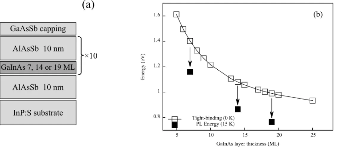
Three GaInAs/AlAsSb multiple quantum-well samples were prepared for the study of their inter-band properties. Their structure is illustrated in figure 2.4a: within each period of these samples, the AlAsSb barrier thickness is fixed to 10 nm, and the GaInAs layer thicknesses is chosen to be 7 ML (sample S1078), 14 ML (S1079) and 19 ML (S1080). Each sample was made to contain 10 periods of quantum wells and no in-tentional doping were applied to the quantum wells. These structures were grown on conductive InP (001) substrates using solid source MBE, under the conditions described in section 1.2 (page 9). To protect the Al-containing layers from oxidation in the air, each of these samples was finished by a 5 nm-thick GaAs0.51Sb0.49 layer.
AlAsSb 10 nm GaInAs 7, 14 or 19 ML ×10 InP:S substrate GaAsSb capping AlAsSb 10 nm
(a)
0.8 1 1.2 1.4 1.6 5 10 15 20 25 E ne rgy (e V)GaInAs layer thickness (ML)
(b)
Tight-binding (0 K) PL Energy (15 K)
Figure 2.4: (a) Structures of samples S1078–S1080 (b) Calculated transition energies (0K)
compared to PL energies recorded at 10 K. The excitation power density was 4 kW/cm2. PL spectra of these samples were recorded under temperature ranging from 15 K
up to about 250 K. A 532-nm laser was used as excitation source and the maximum excitation power density was about 4 kW/cm2. Figure 2.4b presents a comparison of PL peak energies obtained at 15 K along with those tight-binding calculated inter-band transition energies. The PL energies follow the same trend as the calculations but they are systematically lower than calculated values by about 200 meV. Many factors could be responsible for such large difference, including the accuracy of calculations, the error in quantum well thickness and the unintentional incorporation of Sb in GaInAs layer. Precision of quantum well thickness
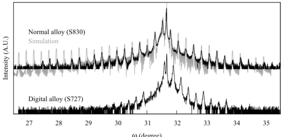
In order to examine the possible deviation of quantum well thickness, the structural parameters of these quantum-well samples were check by X-ray diffraction (XRD). ω−2θ scans were performed to find out the periodic thickness of these quantum wells, namely the thickness of GaInAs layer plus that of AlAsSb layer. All the measured quantum-well periods are found to be smaller than their nominal values by about 4-5 ML. The “missing thicknesses”, that is, the difference between experimentally measured thickness and those intended, are plotted in figure2.5versus their nominal thickness. The ‘missing’ period thickness is actually linearly correlated to the nominal quantum-well thickness. This could be a result of rounding error in MBE growth rate calibration. Since the only varying parameter among all three samples is the GaInAs layer thickness, the slope formed by the three data points thus stands for the error in GaInAs growth rate, which is about 10%. 0 1 2 3 4 5 6 7 0 5 10 15 20 25 “Mi ssi ng T hi ckne ss” (ML )
GaInAs layer nominal thickness (ML) AlAsSb
GaInAs
S1078 S1079
S1080 S830
Figure 2.5: Missing thicknesses in GaInAs/AlAsSb quantum wells.
The error in growth rate calibration can be subtracted by extrapolating the ‘missing thickness’ to zero-GaInAs thickness and the intersection in figure2.5shows that there’s still 3.5 ML missing. To attribute the ‘missing thickness’ to the GaInAs and AlAsSb layers composing each quantum well period, we performed X-ray reflectivity on one of these samples. The result reveals that in each period of Ga0.47In0.53As/AlAs0.56Sb0.44
quantum well sample S1078, about 1.1 ML of thickness is missing from GaInAs layer, and 3.1 ML was missing within the AlAsSb layer. Therefore, out of the 3.5 ML missing, 3.1 ML is contributed by AlAsSb layer, leaving the segregation of indium to be the last possible source of 0.4 ML ‘missing thickness’.
The above structural analysis gives an estimation of the magnitude of indium segre-gation as well as a better growth rate calibration. But the detected thickness error is still too small to cause the observed 200 meV difference between experimental PL energies and calculated inter-band energies.
Unintentional incorporation of Sb
Sb is known to segregate during MBE growth and it can get unintentionally incorporated into layers that next to antimonide alloys. In fact, elemental Sb can stay on the growth front for a while even after its supply is interrupted [25]. To evaluate the Sb-incorporation level in GaInAs/AlAsSb quantum well, we have simulated inter-band transition energy in Ga0.53In0.47As1−ySby /AlAs0.56Sb0.44 single quantum wells using k · p method. In
figure2.6, the calculated energies given in empty squares are compared with PL energies in filled squares. The PL energies seem to coincidence with calculated energies for
y = 20%and the they seem to indicate the unintended Sb-incorporation level in GaInAs
layer could be about 20% , which is unexpectedly high. Microscopic studies is required to confirm such high level of unintentional incorporation of Sb, and this issue will be addressed in later section 2.4using cross-sectional scanning tunneling microscopy.
0.6 0.8 1 1.2 1.4 1.6 1.8 0 5 10 15 20 25 30 E n er g y ( eV ) GaInAs Thickness ( ML ) GaInAs/AlAsSb + Sb S829 T-B GaInAs k.p GaInAs PL GaInAs k.p +Sb 0.1 0.2 0.3 0.5 0.1 0.2 0.3 0.5 0.1 0.2 0.3 0.5
Figure 2.6: Calculated inter-band transition energy under different levels of Sb-incorporation
2.3 Inter-subband properties of Ga
0.47In
0.53As/AlAs
0.56Sb
0.44multiple quantum wells
Effect of doping
Beside good control of quantum well thickness, another important aspect of achieving strong inter-subband transition is to sufficiently populate conduction-band ground state. This is commonly accomplished by high level n-doping using Si. Sheet carrier densities higher than 1 × 1012cm−2 is being used by many research groups [17,19]. For a quan-tum well as thin as 2 nm, it requires a bulk doping level of about 1 × 1019cm−3. We first performed calibration on n-doping in GaInAs with bulk GaInAs sample. With the maximum Si flux and modest GaInAs growth rate of 0.2 ML/s, a doping level of 5 × 1018cm−3 can be achieved.
Being aware that high-level of Si doping could introduce addition disorder at the GaInAs/AlAsSb interface [26,27], two GaInAs/AlAsSb multiple-quantum well samples S1309 and S1310 were prepared to evaluate the impact of doping in such structures. They were elaborated under the same conditions as previous GaInAs/AlAsSb structures and they have the same structures as previous samples except for that the thickness of GaInAs layer is fixed to 7 ML (2.1 nm) . The GaInAs layers in sample S1309 is doped with Si while sample S1310 is kept intact for comparison.
0 500 1000 1500 2000 2500 3000 3500 4000 0.8 0.9 1 1.1 1.2 1.3 1.4 Int ensi ty (c ps) Energy (eV) 20 K S1309 (:Si) S1310
Figure 2.7: Low temperature PL spectra of sample S1309 and S1310. The incident laser power
density was about 4 kW/cm2.
The two samples are characterized by PL from 20 K up to room temperature. Fig-ure2.7displays low temperature PL spectra of these two samples obtained under 20 K, while other PL characteristics are summarized in table 2.1. Compared with the non-doped sample S1310, doping in sample S1309 has led to neither broadening nor additional peaks that were observed in reference [27]. On the contrary, the Si-doped sample has a very similar line width as the non-doped sample. And it even demonstrates higher
Table 2.1: PL characteristics of sample S1309 and S1310
Sample Peak energy (eV) Line width (meV) E24 K 300K 24 K 300 K A (meV)
S1309 1.244 1.21 74 123 25.7
S1310 1.27 1.24 79 121 25.0
thermal activation energy EA for non-radiative process. These PL results indicate no
serious degradation was caused by doping.
Absorption measurement using a multi-pass waveguide
In order to observe the interaction between incident-light and inter-subband transitions, it is necessary to couple the incident-light into transverse-magnetic (TM) mode in the quantum wells. A ridge waveguide illustrated in figure2.2ahas 100% TM-mode coupling efficiency. Nevertheless, fabrication of such a structure requires knowledge in technolog-ical process of AlAsSb; without proper treatment, an AlAsSb-based ridge could oxide by its lateral facets [28] and breaks down in the atmosphere. Alternatively, the multi-ple reflection waveguide is a commonly adopted solution in optical studies, since it can be easily fabricated and yet it has TM-mode coupling efficiency as high as 71% [29]. Figure 2.8 shows a schematic representation of such a waveguide, which is obtained by shaping epitaxial samples into slabs with parallelogram cross-sections.
L D “TM” incidence TE-incidence Ex Ez Ey z x y
Figure 2.8: Geometry of a multi-pass waveguide. Double-headed arrows stand for p-polarized
light whose electric-field vector lies in the paper, and dots represents s-polarized light whose electric-field is perpendicular to the paper.
Due to the strong refraction index contrast between the air and semiconductor ma-terials, the internal surfaces of the waveguide are total-reflective for a large range of angles. Light entering from the facets of parallelogram slabs can propagate along a zigzag path inside the waveguide. For the parallelogram waveguide draw in 2.8, light travels a distance of l =√2L in the guide and it passes through the epitaxial layers 2N times, where N = ⌊L/2D + 1/2⌋. The length of waveguide L has to be sufficiently long so that attenuation due to the absorption of epitaxial layer can be easily detected.
electric field vector is parallel to the in-plane direction (y) with regard to the quantum wells. Its transmittance can be described as
TTE= exp [− (αE1-HH1,y+ αE1-LH1,y+ αothers) · l] (2.3) in which αE1-HH1is absorption coefficient associated with heavy-hole to conduction-band transition. αE1-LH1,y stands for absorption due to the interaction TE-polarized light and light-hole to conduction-band process. 3 All other polarization-independent optical loss
are included in αothers.
When p-polarized light passes through the wave-guide, it transmits in “TM”-mode — which is not exactly the same as the TM-mode in a ridge waveguide. The electric-field of propagating light is 45° away from both z and x directions so that it interacts with both inter-subband (E1-E2) process and inter-band processes (HH1-E1, LH1-E1) :
TTM= exp [
− (α
HH1-E1,x+ αLH1-E1,x+ αothers
2 +
αLH1-E1,z+ αE1-E2+ αothers 2
) · l
]
(2.4) Here, we acknowledge that HH1-E1 process only interacts with electric field vector par-allel to in-plane directions (x and y), while LH1-E1 process interact with both in-plane electric field vector and out-of-planes ones, resulting in absorption coefficients αLH1-E1,x and αLH1-E1,z, respectively 4. Eventually, polarization dependent absorption can be extract by comparing TE and “TM” absorption spectra :
ln TTE(λ)
TTM(λ) = [αinter-subband(λ) − αinterband(λ)] ·
l
2 (2.5)
where all contribution from inter-band process (HH1-E1, LH1-E1) are generalized in
αinterband(ℏω).
The above discussions even apply to situations where inter-band and inter-subband energies are not well separated, and subsequently their contributions to polarization de-pendent absorption cannot be easily isolated. However, in many cases, inter-subband and inter-band energies are well separated. In one hand, at the wavelength range where inter-subband absorption occurs, αHH1-E1 is supposed to be 0 so that in practice log10(TTE/TTM) ∝ αE1-E2 is commonly used to present the inter-subband absorption, which appear as a peak centered at ℏω = E2−E1. On the other hand, at the wavelength range where inter-band absorption occurs, αE1-E2 is supposed to be 0, thus inter-band absorptions αinter-band will appear in log10(TTE/TTM) plot as a valley. The above dis-cussions only apply to perfect quantum wells. In reality, the polarization selection-rules may be relaxed due to asymmetric quantum well profile, strain and all kinds of
inhomo-3Here we only try to deal with transitions related to E
1 or E2; absorption related to higher subband
or inter-valence-band absorption are not taken into account.
4The projections of LH
1–E1 dipole moment along x (y) and z directions are different, so the values
geneity.
The absorption contributed by InP substrate is not yet taken into account in above discussion. InP has a direct band-gap of 1.34 eV at room temperature and it can inter-fere in the measurement of the absorption in two ways. For one thing, inter-subband transition may be submerged in free-carrier absorption background. This can be avoided by using semi-insulating substrate, which has very small free-carrier density. For an-other, the inter-band absorption of a GaInAs/AlAsSb quantum well may overlap with absorption originating from InP direct gap. As is indicated in figure 2.3, inter-band absorption energy of a 5 ML GaInAs/AlAsSb quantum well is already very close to the band-gap of InP. To better resolve the inter-band absorption spectra near band-gap of InP, we used a reference scheme to subtract the absorption contributed by the substrate. Each multi-pass waveguide is actually further divided into two equal parts by its width. One piece stays intact and it becomes a ‘test’ sample for absorption measurement. The other ‘reference’ sample goes through wet-etching process so that its epitaxial layers are removed. Eventually the part of absorption contributed by InP substrate can be removed by comparing the absorbance spectra of ‘test’ and ‘reference’ samples.
Reduction of barrier layer thickness
Another way to increase inter-subband absorbance is to integrate more quantum wells in the structure. Since all materials in Ga0.47In0.53As/AlAs0.56Sb0.44 quantum wells are lattice-matched to InP substrate, there’s no major difficulty in achieving arbitrary thick structure. But it would be beneficial to reduce the thickness of AlAsSb layer in order to reduce growth time of samples with high stacking-number.
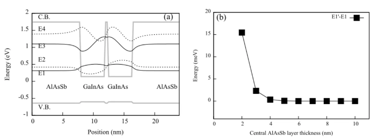
Here we try to determine the minimum AlAsSb layer thickness that is required to sufficiently separate two GaInAs quantum wells. We examine two Ga0.47In0.53As quantum wells separated by a variable central barrier using k ·p calculations.Figure2.9a shows the band schema of such a structure, and the energy split between the first two eigenstates E2− E1 was used an indication of the strength of the coupling between the two quantum wells. Figure2.9bdisplays the energy split as a function of central barrier thickness. E1 and E2 are mostly degenerated until the barrier thickness is reduced to about 5 nm. Thus 6 nm thick AlAsSb layers is considered sufficient and this value is used in future GaInAs/AlAsSb samples prepared for inter-subband absorption studies. Near-infrared Absorption of Ga0.47In0.53As/AlAs0.56Sb0.44
Samples preparation
Three Ga0.47In0.53As/AlAs0.56Sb0.44 multiple quantum well samples were prepared for the study of inter-subband absorption. Figure 2.10a illustrates the structure of these samples, in which the AlAsSb layer is now reduced to 6 nm. The three samples have
-1 -0.5 0 0.5 1 1.5 2 0 5 10 15 20 E ne rgy (e V) Position (nm) (a) C.B. E4 E3 E2 E1 V.B.
AlAsSb GaInAs GaInAs AlAsSb
0 5 10 15 20 0 2 4 6 8 10 E ne rgy (m eV)
Central AlAsSb layer thickness (nm)
(b) E1'-E1
Figure 2.9: The determination of minimal AlAs0.56Sb0.44barrier layer thickness. (a) In coupled-double quantum wells, the split between originally degenerated levels E2-E1 serves as an indi-cation of coupling between them. (b) Calculated energy split as a function of central barrier thickness.
5 ML (S1346), 7 ML (S1329) or 9 ML (S1347) of GaInAs in each period of their quantum wells. These samples were grown under the same conditions as previous ones except that semi-insulating InP:Fe substrate was used to suppress free-carrier absorption in the substrate, and the GaInAs layers are intentionally doped with Si (5 × 1018cm−3) to populate conduction-band ground-level. To increase the inter-subband absorbance, the number of quantum well contained in these samples is now increased to 100. To protect surface AlAsSb layer from oxidation, all the samples were finished with a 5 nm thick GaAs0.51Sb0.49 layer.
After the growth, the samples are made into multiple reflection waveguides: they are first thinned to a thickness of about 280 µm and cleaved into slabs around 8 mm wide and 16 mm long. After a series of mechanical polishing and chemical etching, they are shaped into multi-reflection ‘test’ samples and their accompanying ‘reference’ samples without epitaxial layer. The photo in figure A.2(page 119) gives an example of such a multi-reflection waveguide.
Room PL characteristics
To assure that the optical qualities of these samples were not degraded during mechan-ical processing, PL experiments were performed on the epitaxial side of these multiple-reflection waveguides. Figure 2.10b shows room temperature PL spectra of these sam-ples. They are actually as strong as unprocessed samples and this assures the integrity of epitaxial layer. The PL spectra of sample S1329 (7ML) has a line-width of 84 meV , which is actually not broader than that of a similar 10 periods sample (S1309). This suggests the no extra inhomogeneity has developed during the stacking of large number of quantum wells. The PL peak of sample S1346 (5 ML) is centered at 950 nm, which is not far from the absorption edge of InP substrate as well as the limit of our spectrometer.

![Figure 2: Band line up of several ternary alloys that are lattice matched to InP. Data are taken from [9].](https://thumb-eu.123doks.com/thumbv2/123doknet/14528555.723226/11.892.181.648.160.431/figure-band-ternary-alloys-lattice-matched-data-taken.webp)