HAL Id: hal-01745633
https://hal.archives-ouvertes.fr/hal-01745633
Submitted on 28 Mar 2018
HAL is a multi-disciplinary open access archive for the deposit and dissemination of sci-entific research documents, whether they are pub-lished or not. The documents may come from teaching and research institutions in France or abroad, or from public or private research centers.
L’archive ouverte pluridisciplinaire HAL, est destinée au dépôt et à la diffusion de documents scientifiques de niveau recherche, publiés ou non, émanant des établissements d’enseignement et de recherche français ou étrangers, des laboratoires publics ou privés.
On the electrical variability of resistive-switching
memory devices based on NiO oxide
S Tirano, Marc Bocquet, Christophe Muller, D. Deleruyelle, L. Perniola, V.
Jousseaume, B. de Salvo, G. Reimbold
To cite this version:
S Tirano, Marc Bocquet, Christophe Muller, D. Deleruyelle, L. Perniola, et al.. On the electrical variability of resistive-switching memory devices based on NiO oxide. 2011 IEEE 42nd Semiconductor Interface Specialists Conference (SISC), Dec 2011, Arlington, United States. �hal-01745633�
On the electrical variability of resistive-switching memory devices based on NiO oxide
S.Tirano a,b, M.Bocquet a, Ch.Muller a, D.Deleruyelle a, L.Perniola b, V.Jousseaume b, B. De Salvo b,
G.Reimbold b
a IM2NP, UMR CNRS 6242, Aix-Marseille Université, F-13451 Marseille Cedex 20, France b CEA-LETI, MINATEC Campus, 17 rue des Martyrs, F-38054 Grenoble, France
Resistive-switching memories (so-called RRAM) are increasingly investigated since they gather low cost, high integration capabilities together with good performances [1]. RRAM memories based on transition metal oxide are promising candidate because of a simple metal/oxide/metal stack allowing the integration of memory elements into the back end of line [2]. Before substituting conventional Flash memories, RRAM devices must fulfill reliability requirements and the variability of their electrical characteristics has to be properly apprehended. In this paper the variability on forming and reset characteristics are
reproduced by 1D modeling. By using this approach, this paper aims at identifying the key physical parameters that may explain the intrinsic spread of electrical characteristics.
As depicted in Fig.1, RRAM devices consist of a NiO active layer (25nm thick) sandwiched between two platinum electrodes (25nm thick). Such devices exhibit unipolar resistive switching effect between two conductivity states, i.e. a low resistance state (LRS) and a high resistance state (HRS) [3]. To identify the conduction mechanism in the pristine state, current-voltage characteristics were accurately measured at various temperatures. Below the forming voltage (zone III in Fig. 2a), the current does not show evident thermal activation that may be in agreement with a trap-assisted tunneling (TAT) mechanism described here in terms of barrier height (B) and average distance between traps (w) [6]. Figure 3 shows the
max/min and median dc IV characteristics measured on several RRAM either during the forming stage (Fig. 3a) or during the reset operation (Fig. 3b). Finally in Fig. 4 forming and reset voltages are monitored with respect to environing temperature (these are first data ever shown in the literature, to our knowledge, on this aspect). To apprehend the impact of physical parameters on the intrinsic variability of electrical characteristics, a self-consistent physical model accounting for both forming and reset operations was used [4]. This model takes into account two distinct mechanisms: a redox reaction (i.e. electrochemical oxidation/reduction processes) during forming, and thermal diffusion and dissolution of conductive filaments (CFs) during reset [5]. In Table 1, the impact on electrical characteristics is evidenced for each physical parameters. Microscopical parameters related to TAT conduction (B and w) and the free energy
of the reduction reaction at equilibrium (Ered) mainly affect the forming voltage. In contrast, the activation
energy of the LRS (Ea) involved in the dissolution of CFs and retention characteristic, together with
electrical parameters related to the CFs (resistivityCF0, thermal conduction KthCF, thermal coefficientT)
largely affect the reset voltage and the reset current. Another important parameter is the current compliance during forming Icomp that strongly influences reset current and resistance in LRS [7]. Indeed
Icomp must be controlled to avoid larger spread of electrical characteristics [8]. Provided these elements,
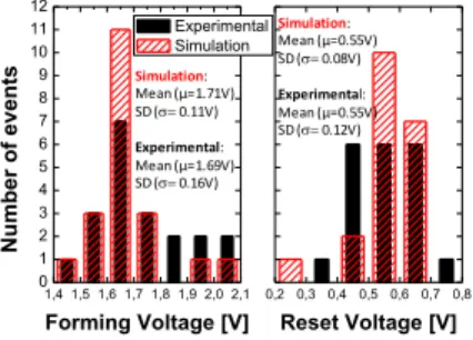
the mean values (ie µ) of different parameters were calibrated on the median IV, for forming and RESET (Fig 3); then slight variation (ie ) on each of them allowed a good fit on min/max characteristics, as evidenced in Fig. 3 and Fig. 5 on large set of data: in Table II the set of µ and are highlighted. Note that in Table II a quantitative view of the impact of each microscopical parameters is provided in the last column. Eventually in Fig. 4 we compare modeling result on random set of physical parameters (with µ and from Table 2) with data. We obtain a fine agreement with data, that could be improved enlarging the statistical ensemble of data.
To summarize, the present work enables apprehending the impact of physical parameters on the variability of NiO-based RRAM. The important variability of current in pristine state may be linked on variation of NiO layer during fabrication process which impacts the barrier height (B) and average
parameters (CF0 and KthCF) and can explain the variability in LRS for current and reset voltage. Also the
impact of each microscopical parameter has been quantitatively put in relation with the macrocopical electrical counter-part.
References
[1] I. G. Baek et al., IEDM Technical Digest, (2004) 587–590. [2] M-D. Lee et al.,Transaction on Magnetics, 43 (2) (2007) 939–942 [3] V. Jousseaume et al., Solid-State Electronics, 58 (1) (2011) 62–67. [4] M. Bocquet et al., Appl. Phys. Lett., 98 (2011) 263507.
[5] U. Russo et al., Transaction on Electron Devices, 56 (2) (2009) 193–200.
[6] Gushterov et al., J. Optoelectronics Advanced Materials, 7 (3) (2005) 1389–1393. [7] F. Nardi et al., Solid-State Electronics, 58 (1) (2011) 42–47.
[8] S. Tirano et al.,Microelectronic Engineering, 88 (7) (2011) 1129–1132.
NiO (25nm) Pt (25 nm) Pt (25 nm) Ti (10 nm) TiN (40 nm) TiN (10 nm) W AlCu 300 nm 1.2 µm 0,0 0,5 1,0 1,5 2,0 10-10 10-9 10-8 10-7 10-6 10-5 10-4 Curr ent [A] Voltage [V] 0,01 0,1 1 10-10 10-9 10-8 10-7 Curr ent [A] Voltage [V] 25°C 50°C 75°C 100°C 125°C 150°C I II III a) b) 0 1 2 10-11 10-10 10-9 10-8 10-7 10-6 10-5 10-4 Curr ent [A] Voltage [V] Symbol - Experimental Line - Simulation a) b) 0,0 0,1 0,2 0,3 0,4 0,5 0,6 1,0x10⁻³ 2,0x10⁻³ 3,0x10⁻³ 4,0x10⁻³ Symbol - Experimental Line - Simulation Current [ A] Voltage [V] Figure 1: Schematic description of the NiO-based RRAM memory elements.
Figure 2: a) Typical current-voltage characteristic
measured from the pristine state. Zone I: no resistance switching; Zone II onset resistance switching; Zone III switching event to LRS. b) Temperature-dependent evolution of current at low voltage.
Figure 3: Extreme-value current-voltage characteristics
measured either in the forming stage a) or during the reset operation b). Each experimental curve is satisfactorily fitted by the unipolar switching model.
300 350 400 450 500 0,2 0,4 0,6 0,8 1,0 1,2 1,4 1,6 1,8 2,0 Vre s e t / V formi ng Temperature [K] Simulation Experimental Vforming Vforming Vreset Vreset
Parameters Electrical impact
Fo rmi n g im p ac t φB(eV) HRS current w (nm) HRS current
Ered(eV) Forming voltage
R
e
se
t
KthCF(W/K*m) Reset voltage
Ea(eV) Thermal activation of LRS retention Icomp(mA) Resistance in LRS
αT(1/K) Ohmic behavior in LRS
ρCF0(Ω*m) Reset voltage and Resistance in LRS
Figure 4: Forming and reset voltage behavior with respect to temperature for
experimental and simulation.
Table 1: Electrical impact of parameters for forming and reset
operation
Parameters Mean Value (µ)
Standard Deviation ( σ )
Impact on electrical property of each parameter [ µ-σ ; µ+σ ] Fo rmi n g im p ac t φB (eV) 0.390 0.045 ( +σ ) ÷3.065 HRS current ( -σ ) x3.065 HRS current w (nm) 3.550 0.350 ( +σ ) ÷3.370 HRS current ( -σ ) x3.370 HRS current Ered (eV) 3.05 0.30 ± 15% on Vforming R e se t im p ac t KthCF (W/K*m) 30 5 ± 5% on Vreset Ea (eV) 1.10 0.11 ± 6% on Vreset Icomp
(mA) 5 1 ± 20% on Ireset and LRS current
αT
(1/K) 0.5e-3 0.1e-3 ± 7% on LRS current
ρCF0 (Ω*m) 0.7e-5 0.2e-5 ± 10% on Vreset ± 5.71% on RLRS 1,4 1,5 1,6 1,7 1,8 1,9 2,0 2,1 0 1 2 3 4 5 6 7 8 9 10 11 12 Experimental Simulation Number o f eve nts Forming Voltage [V] 0,2 0,3 0,4 0,5 0,6 0,7 0,8 Reset Voltage [V] Simulation: Mean (µ=1.71V) SD (=0.11V) Experimental: Mean (µ=1.69V) SD (=0.16V) Simulation: Mean (µ=0.55V) SD (=0.08V) Experimental: Mean (µ=0.55V) SD (=0.12V)
Table 2: Mean value (µ) and standard deviation () of physical parameters used to fit experimental data (Fig 3-4). Impact on electrical characteristics due to an independent variation of each physical parameters in forming and reset operations
Figure 5: Experimental and simulated dispersions of forming