Distributed Algorithms for Self-Disassembly in
Modular Robots
by
Kyle W Gilpin
Submitted to the Department of Electrical Engineering and Computer
Science
in partial fulfillment of the requirements for the degrees of
Bachelor of Science in Electrical Science and Engineering
and
Master of Engineering in Electrical Engineering and Computer Science
at the
MASSACHUSETTS INSTITUTE OF TECHNOLOGY
June 2006
@Kyle
W Gilpin, 2006.
The author hereby grants to M.I.T. permission to reproduce and
distribute publicly paper and electronic copies of this thesis and to
arnf. n .hprQ thp ri cht tfn drn Qn
Author ... .'-. ...--- ...
Department of Electrical Engineering and Computer Science
May 26, 2006
Certified by... ... -. ... ...
Daniela Rus
Associate Professor of Electrical Engineering and Computer Science
.Tesi5sSupervisor
Accepted by ... ;. .
Arthur C. Smith
Chairman, Department Committee on Graduate Students
ARCHIVES
MASSACHUSETTS INSTMITEOF TECHNOLOGY
AUG 1 4 2006
.... LLBRARIES
Distributed Algorithms for Self-Disassembly in Modular
Robots
by
Kyle W Gilpin
Submitted to the Department of Electrical Engineering and Computer Science on May 26, 2006, in partial fulfillment of the
requirements for the degrees of
Bachelor of Science in Electrical Science and Engineering and
Master of Engineering in Electrical Engineering and Computer Science
Abstract
We developed a modular robotic system that behaves as programmable matter. Specifically, we designed, implemented, and tested a collection of robots that, starting from an amorphous arrangement, can be assembled into arbitrary shapes and then commanded to self-disassemble in an organized manner.
The 28 modules in the system were implemented as 1.77-inch autonomous cubes that were able to connect to and communicate with their immediate neighbors. Two cooperating microprocessors controlled the modules' magnetic connection mecha-nisms and infrared communication interfaces.
We developed algorithms for the distributed communication and control of the system which allowed the modules to perform localization and distribute shape infor-mation in an efficient manner. When assembled into a structure, the modules formed a system which could be virtually sculpted using a computer interface which we also designed. By employing the sculpting process, we were able to accurately control the final shape assumed by the structure. Unnecessary modules disconnected from the structure and fell away.
The results of close to 200 experiments showed the that the algorithms operated as expected and were able to successfully control the distributed system. We were able to quickly form one, two, and three dimensional structures.
Thesis Supervisor: Daniela Rus
Acknowledgments
I owe a great deal of gratitude to Daniela Rus for her support throughout the last year. This project never would have come to fruition without the help of my colleagues in the Distributed Robotics Lab. In particular, I am indebted to Iuliu Vasilescu who provided the impetus for the algorithms that I developed as well as countless hours soldering and assembling the modules. Keith Kotay also deserves special recognition for the time he spent discussing and prototyping the early connector mechanisms. Finally, I would like to thank my parents, Linda and Bill, who both read this thesis and provided excellent feedback.
This thesis was made possible by support from NSF, Air Force MURI, Intel, and a generous donation of connectors by Magswitch Technology, Inc.
Contents
1 Introduction
2 Related Work
3 Hardware
3.1 Processors . ...
3.1.1 Primary ARM Processor ...
3.:1.2 Secondary PSoC Processor ...
3.2 Connection Mechanism ... 3.3 Communication Interface ... 3.4 Orientation Detector . ... 3.5 Power Regulators ... 4 Low-Level Software 4.1 I2C Communication ... 4.1.1 I2C Commands ... 4.2 Magswitch Control ...
4.2.1 Threshold-Based Magswitch Control
4.2.2 Slope-Based Magswitch Control .
4.3 Inter-Module Message Transmission ...
4.3.1 Message Format ...
4.3.2 Message Structure ...
4.3.3 Message Buffering ...
7
4.4 4.5
Inter-Module Message Reception . . . .
Basic Message Types . ... .
4.5.1 Acknowledge (ACK) Messages ...
4.5.2 Not Acknowledge (NCK) Messages ...
4.5.3 Disconnect All Magswitches(DCA) Messages.
4.5.4 Disconnect Request (DRQ) Messages ...
4.5.5 Magswitch State (MSS) Messages . . . .
4.5.6 Reset (RST) Messages . ...
4.5.7 Real Time Clock (RTC) Messages . . . .
5 Self-Disassembly Algorithms 5.1 Neighbor Discovery ...
5.2 Localization ... ... ...
5.2.1 Localization Message Propagation . . . .
5.2.2 Reflection Messages .. . . . . . . ..
5.2.3 Correctness of the Localization Algorithm . .
5.2.4 Running Time of the Localization Algorithm .
5.3 Inclusion Message Generation . . . .
5.3.1 Constructing the Graph . . . .
5.3.2 Finding Shortest Paths . . . . . . ..
5.3.3 Generating the Inclusion Messages . . . . 5.4 Shape Distribution ...
5.4.1 Inclusion Message Propagation . . . .
5.4.2 Shape Distribution Correctness . . . . 5.4.3 Running Time of the Shape Distribution Algorithm 5.5 Disassembly ...
5.5.1 Disassemble Message Propagation ...
5.5.2 Correctness of the Disassembly Algorithm ... 5.5.3 Running Time of the Disassembly Process ...
55 56 56 57 58 58 59 59 60 61 62 ... . 63 . . . . . 63 .. . . . . . 65 . . . . . 66 . . . . . 68 . . . . . 69 . . . . . 70 . . . . . 71 . . . . . 72 ... . 73 . . . . . 73 . . . . . 77 . . . . . . 79
6 Algorithm Implementation 83
6.1 Increasing System Reliability ... ... . 83
6.1.1 Synchronization ... .... ... 85
6.1.2 Localization Modification ... . . . . . 87
6.1.3 Shape Distribution Modification . ... 88
6.2 Message Specification ... ... 89
6.2.1 Ping (PNG) Messages ... ... 89
6.2.2 Localization (LOC) Messages . ... 90
6.2.3 Reflection (REF) Messages . ... . 90
6.2.4 Inclusion (INC) Messages ... .. 91
6.2.5 Disassemble (DAS) Messages . ... 92
6.3 Graphical User Interface ... . 93 7 Experimental Results
7.1 Neighbor Discovery Results . . . ..
7.2 Localization Results ...
7.3 Inclusion Message Generation Results . . . . . . . . . ....
7.4 Shape Distribution Results . . . . . . . . ..
7.4.1 Running Time Comparison . . . . . . . ..
7.5 Disassembly Results . . . . . . . . . . ..
8 Conclusions
8.1 Hardware Lessons Learned . . . . . . . . ..
8.2 Software Lessons Learned . . . ..
A Schematics
B ARM Source Code
B.1 main.c ... .. ... ... B.2 handlemsg.c . ... . . . . . . . .. B.3 txmisg.c ... . . ... ... B.4 crc.c ... .. .... ... 97 98 98 103 104 109 110 113 113 114 117 125 125 127 140 145
. . . 146 B.6 msgqueue.c ... .. ... 152 B.7 debug.c ... ... 156 B.8 usrint.c... ... ... 169 B.9 log.c ... ... 174 B.10 rtc.c ... ... . ... 177 B.11 eeprom.c ... ... 181 B.12 psoc.c ... ... 186 B.13 i2c.c ... ... 193 B.14magswitch.c ... ... 196 B.15 orientation.c .. . .. . .. ... . .. ... .. .. .. .. .. .. .. . 202 B.16 tmrl.c ... 205 B.17 uart.c ... ... ... . ... 207 B.18 ioctrl.c ... ... 210 B.19 clocks.c ... ... 211 B.20 util.c ... .... . ... . ... 213
C PSoC Source Code 215 C.1 main.c ... 215 C.2 i2c.c ... ... 215 C.3 comparator.c ... 219 C.4 tx.c ... .. ... 221 C.5 rx.c ... 222 C .6 hall.c . . . . . . .. . 223 B.5 parsemsg.c
List of Figures
1-1 Initial and final configurations of a self-disassembling system .... . 19
3-1 A single self-disassembling module . ... 27
3-2 The inside of a self-disassembling module . ... 28
3-3 ARM processor block diagram ... ... 30
3-4 PSoC processor block diagram ... 32
3-5 A single Magswitch connector ... 35
3-6 Magswitch drive chain ... ... 36
3-7 Magswitch and Hall Effect sensor arrangement . ... 37
3-8 Hall Effect sensor output voltage vs. Magswitch rotation ... . 38
3-9 Photodiode output voltage vs. distance . ... 40
3-10 Photodiode output voltage vs. alignment offset . ... 40
4-1 Low-level message processing loop . ... . 44
4-2 Hall Effect sensor output voltage variance . ... 48
4-3 Slope-based Magswitch control algorithm . ... 50
4-4 Basic inter-module message format . ... 53
4-5 Acknowledge (ACK) message format . ... 57
4-6 Magswitch state (MSS) message format . ... 59
4-7 Real time clock (RTC) message format . ... . . 60
5-1 Four phases of self-disassembly ... .. 61
5-3 Constructing a graph for the shape distribution message generation 5-4 5-5 5-6 6-1 6-2 6-3 6-4 6-5 6-6 6-7 process ... . ...
Constructing a breadth-first tree . . . Evolution of a single inclusion message Shape distribution process ...
Complete software heirarchy . . . . Ping (PNG) message format . . . . Localization (LOC) message format . . . Reflection (REF) message format . . . . Inclusion (INC) message format . . . . Disassemble (DAS) message format . . . Graphical user interface screen capture
7-1 Time required for a chain of modules to receive localization messages 7-2 Time required for a chain of modules to transmit reflection messages
back to the GUI during localization ...
7-3 Time required for a square of modules to receive localization messages 7-4 Time required for a square of modules to transmit reflection messages
back to the GUI during localization . . . . 7-5 Time required for a cube of modules to transmit reflection messages
back to the GUI during localization ...
7-6 Time required by the GUI to generate a sequence of inclusion messages for a chain of modules ...
7-7 Time required for a chain of modules to receive inclusion messages . . 7-8 Time required for a chain of modules to transmit reflection messages
back to the GUI during shape distribution . . . . 7-9 Time required for a square of modules to receive inclusion messages 7-10 Time required for a square of modules to transmit reflection message
back to the GUI during shape distribution . . . . 7-11 Time required for a cube of modules to receive inclusion messages . .
. . . . . 84 . . . . . 90 . . . . . 90 . . . . . 91 . . . . . 92 . . . . . 93 . . . . . 94 100 100 101 101 102 104 106 106 107 108 108 . . .. . . .. . .. . . .. . . 7 1 . . . . . 72 . . . . . 76 . .. . . .. . . .. . .. . . . 77
List of Tables
4.1 I2C commands ... ... ... 46
4.2 Comparison of the threshold-- and slope-based Magswitch control
al-gorithms ... ... ... 52
5.1 A depth-first search generates a sequence of inclusion messages . . . 73
Chapter 1
Introduction
Self-organization is the ability of distributed systems to form functional groups and structures in accordance with their environment and task. Self-organizing systems serve as tools which can be used to simulate the interaction of simple behaviors that, when aggregated, display surprisingly complicated phenomena. The systems are highly relevant and potential laden due to their similarities with numerous biological systems such as those of social insects and nervous systems. Consequently, artificial self-organizing systems can assist scientists in gaining a better understanding of the natural world and extracting information which can be utilized to better society.
This thesis looks at self-organizing systems which are able to self-disassemble. That is, they are able to transform from regular homogeneous structures into more intricate and interesting configurations by removing some system components. The basic idea behind the self-disassembling modules we developed can be thought of as sculpting a block of marble. A prearranged structure of individual modules will transform into a different structure by breaking apart in an orderly fashion. Much like a sculptor would remove the extra stone from a block of marble to reveal a statue, our self--disassembling system eliminates unnecessary modules to form a more interesting structure.
A collection of millions of modules, if each were small enough, could form a pletely malleable building material that could solidify and then disassemble on com-mand. The applications for such a material are numerous. For example, the material
could be applied to help heal severely broken bones that would otherwise require the use of permanent steel plates or pins. Thousands of tiny modules could be packed around the break by a surgeon, or they could be injected into the body and drawn to the site of the break with a magnetic field. Once satisfied that enough modules surrounded the break, the modules could be instructed to solidify. The solid struc-ture of modules would both immobilize the broken bone and provide a scaffolding on which new bone material could regenerate. The modules would also be able to sense the bone's regrowth and slowly disassemble in the places they were no longer needed. The modules could also provide feedback detailing how well the bone was mending. The disassembly process would continue until the two pieces of bone were securely re-attached. As the modules disassembled from the structure around the site of the break, they could be absorbed into the blood stream and passed out of the body in a harmless manner. While this level of sophistication is still far off, the system we developed serves as a means to study the algorithms the would be necessary for such a use.
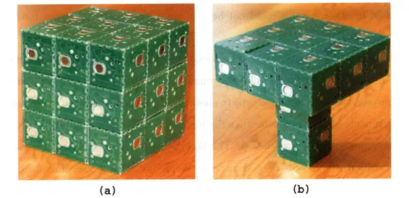
In the particular system we developed, many small modules are initially arranged by hand to form a super-structure, for example, the 27-module cube shown in Fig-ure 1-1(a). Each individual module is physically linked to up to six neighbors. After the super-structure is assembled, we model a desired final configuration of the sys-tem using a desktop computer. This model is transmitted to the structure where it is distributed. Once the super-structure receives information about the desired final configuration of the modules, the appropriate modules break their connections with their neighbors and disconnect from the structure. The unnecessary modules continue to separate until the desired final configuration, pictured in Figure 1-1(b), is achieved.
In the process of implementing our system, we faced numerous hardware design, control, and coordination challenges. When dealing with large self-organizing sys-tems, there are many unsolved problems. We do not yet understand the most efficient way to communicate with all of the modules in a system, nor do we understand how
(a)
(b)
Figure 1-1: A self-disassembling system can transform from an initial uniform as-sembly of identical modules, (a), into a more interesting and functional asas-sembly in
(b).
needed to investigate the emerging properties of distributed, self-organizing systems. Researchers have yet to develop the communication and control algorithms necessary to successfully employ large distributed robotic systems for the study of natural phe-nomena. Additionally, studying self-organization presents challenges because it re-quires vast systems and robust algorithms capable of adaptive, task-driven distributed coordination and control. Methods of fabricating, programming, and debugging such systems do not exist.
Other groups have focused on self-assembling, self-reconfiguring, and self-replicating systems, but little research has been devoted to the specifics of self-disassembly. To study self-disassembling systems, we first had to design appropriate hardware that was as small as possible. In the design process, we imposed the additional constraint that the modules be completely autonomous-each module should have its own sens-ing, processsens-ing, actuation, and power supply capabilities. This choice differentiates our system from several other modular robotic systems that are also under develop-ment. Rarely do modules contain their own power supplies, and many are not able to perform any significant amount of processing. Because we wanted each module to contain its own power source, the standard mechanical and electromagnetic
connec-tors used in other systems could not be employed because they consume too much power.
There were also several challenges associated with designing the software that con-trols the modules. We had to develop communication algorithms that were able to reliably pass messages from one cube to another. When these failed due to mechanical misalignment, we had to ensure that the high-level algorithms that control the dis-assembly process were not affected. The high-level self-disdis-assembly algorithms also needed to operate in a distributed manner. We decided that it was unrealistic for a module to have any global information about the system. Individual modules should only know about the existence and state of their immediate neighbors. Even though the modules did not have information about the system as a whole, they needed to localize with respect to one another and be able to route shape distribution messages throughout the entire structure. Despite these hardware and software challenges, we developed a successful modular self-disassembling system that can serve as a platform for further study.
This thesis is divided into eight chapters. After this first chapter, the second ad-dresses some related work. Chapter 3 then begins to discuss the specifics of the mod-ules we developed by presenting their hardware platform. Following the discussion of the hardware, Chapter 4 explains the important aspects of the low-level software. This software interfaces with the hardware and allows the top-level self-disassembly algorithms to control the modules in a more abstract manner. Chapter 5 presents the basic self-disassembly algorithms, proves that they operate correctly, and analyzes their running times. To actually implement the algorithms on the hardware, we had to incorporate several refinements. These changes and the additional details explain-ing how the algorithms were implemented on the hardware are discussed in Chapter 6. Following the discussion of how the algorithms were implemented, Chapter 7 presents the results of close to 200 experiments that we performed to test the system's abilities and verify that the algorithms operated correctly. Finally, Chapter 8 draws several conclusions about the system and presents directions for future work.
Chapter 2
Related Work
Our work draws on prior and ongoing research in modular and distributed robotics. Specifically, we have built upon work in the fields of self-assembling and self-reconfiguring robotics to develop a new type of system that behaves as programmable matter. To date, only a limited amount of research has been devoted to self-disassembling sys-tems. Most research has focused on self-assembly and self-reconfiguration in robotic systems. Typically, these systems construct and rearrange themselves in order to pro-vide locomotion or to manipulate objects. The topic of this thesis, self-disassembly, can be viewed as a specialized case of reconfiguration, so the research of self-reconfiguring robotic systems is still relevant. In what follows, we summarize several modular systems which have already been developed.
Yoshida presents an intriguing self-reconfiguring system which uses shape mem-ory alloy (SMA) springs to connect neighboring modules [16]. He states that he chose SMA based actuators because they maintain a favorable power to weight ratio when miniaturized. In fact, his smallest modules fit inside a 2 centimeter cube and weigh only 15 gramns. Yoshida's system, which is currently confined to two dimensions, con-sists of square modules that include two male connectors, (on opposing vertices), and two female connectors, (on the opposite set of opposing vertices). The male connec-tors can swing through a 180 degree arc and bond with their female counterparts. This design allows one module to traverse around the exterior of a number of other connected modules. One drawback to Yoshida's system is the amount of power it
consumes. While the system's connectors do not dissipate power in their static state, actuation requires 1 Amp. Consequently, the modules do not contain their own power supplies. Furthermore, all of the processing required for the system's motion planning is performed on a separate computer after which control commands are transmitted to the individual modules [16].
In a separate paper, Yoshida devotes additional space to describing a
three-dimensional adaptation of his system [15]. Additionally, he presents a recursive
method for describing the structures formed by modular robots. This recursive repre-sentation uses multiple layers of abstraction in order to separate the low-level details of the structure from the structure's general shape. For example, eight modules could be arranged to form a cube which is then viewed as a single, indivisible node by higher level descriptions of the system as a whole. Yoshida states that using such a recursive representation enables one to describe sizable, complicated shapes which would be impossible to characterize otherwise.
In [8], Rus describes a system of "crystal" modules which can expand and contract two of their dimensions by a factor of two. The crystal modules are composed of four movable faces arranged in a square. Two of these faces contain active connectors and two contain passive connectors. The active connectors can mate with passive connectors. By selectively latching and unlatching from their neighbors, a collection of crystals is able to arbitrarily modify its structure in two dimensions. In total, each crystal module has only three degrees of freedom: one to expand the faces and two to control the state of the latches on the active faces. Rus presents detailed algorithms to accompany the crystal hardware. These algorithms prove that composite crystal structures can assume arbitrary configurations and that any individual module can relocate anywhere in the structure.
A novel system for self-assembly and reconfiguration is presented by White [13] which uses fluid flow to bind individual modules together. In particular, the modules have gated inlets which, when opened, draw in fluid to exert a suction force on the neighboring modules. Unfortunately, the modules only operate in fluids more viscous than air, such as oil and water. Additionally, the modules have limited processing
power and depend on an external pump to move the fluid and provide the suction force. According to the authors, the greatest advantage of their system is its ability to function correctly even if the modules are shrunk to the microscale [13], a property absent in most self-reconfiguring systems.
The CHOBIE robot developed by Koseki [6] is also unique in its mechanical design. The modules in the CHOBIE system, which are rectangular, are able to locomote by sliding in two planes relative to one another. A module cannot only slide horizontally across the top of another module, but vertically down a module's side as well. This ability allows one robot to climb up and over another. While the CHOBIE robots contain only basic processing power, they are self-contained and able to operate untethered. The system is still confined to two dimensions.
Mytilinaios presents an especially clever system of modular robotics in [7] which is able to self-replicate. The system is composed of cubes that have a rotational degree of freedom in line with the diagonal from one corner of the cubic modules to the corner farthest away. The system uses electromagnets to connect neighboring modules and two electrical contacts to share power and communication signals. Mytilinaios uses the system to investigate different initial configurations that, when given a supply for spare modules, can replicate themselves. As with other systems, the disadvantage of Mytilinaios' system is the apparent inability of the modules to perform high-level computation and the fact the the modules must be anchored to a special base which supplies the necessary power.
While most of the above research efforts focused on modular systems which are completely homogeneous, systems with multiple types of modules also exist. Yim presents the PolyBot system, which relies on two types of modules: segments and nodes [14]. The nodes are passive cubes that have connectors on all six faces. In contrast, the segments consist of only two connectors which are able to move relative to one another. Specifically, a rotational joint driven by a motor separates the two connectors. The PolyBot is a chain type reconfigurable modular robot. In other words, chains of modules connect in order to form structures such as loops, legs, or tendrils. Yim's system has the ability to achieve locomotion through any number
of configurations. For example, a number of segment and node modules can form a loop that rolls across smooth terrain. If confronted with more challenging terrain, the robot can reconfigure itself as a multi-legged walking robot. The PolyBot is also unique because its connectors are not of a specific gender. Using a system of pins and latches, any connector face can mate with any other connector face.
Castano developed another chain-type modular robotic system called Conro that is detailed in [1]. The Conro robot is able to assume forms that resemble snakes and multi-jointed walkers. The Conro system is completely self-contained. Each module has a microprocessor, a power supply, sensing capabilities, communication interfaces, and actuation mechanisms that allow modules to both flex and join together. In fact, each individual module can be considered a robot by itself.
Finally, Kamimura et. al. have developed the M-TRAN modular robotic system [5]. The M-TRAN system is able to use numerous cooperating modules to, among other tasks, achieve a modular walking robot. The individual modules contain two degrees of freedom. In addition, they contain processing and battery power. The most interesting aspect of the M-TRAN system is the way in which it is controlled using a set of interconnected oscillators that are all out of phase with respect to one another. By optimizing the phase relationships between the oscillators, they can be used to drive the modules' motors in a coordinated fashion that leads to forward locomotion. The M-TRAN robot relies on evolutionary algorithms to perform this optimization process. The optimization process can occur in simulation before being implemented in hardware, or it can be performed in real-time to allow the robot to adapt to a changing environment [5].
The modular system presented in this thesis is different from all of the above systems for several reasons. First, the system presented here focuses on the process of self-disassembly. Unlike most existing systems which must find creative ways to compress or hide extra modules, the system presented here disposes of extra modules. Second, the system operates in three dimensions. The modules have no preferential direction and can be assembled into arbitrary structures. Third, the modules we developed contain significant amounts of processing and battery power. If necessary,
this allows the modules to play a significant role in the process of shape planning and distribution. The modules' autonomous nature also enables any structure they com-pose to continue to perform sensing and computation even after the self-disassembly process is complete. Finally, this thesis explores several novel algorithms that com-municate structural data about the system to a user interface and information about the structure's desired configuration back to the modules.
Chapter 3
Hardware
The self-disassembling system that we developed is composed of autonomous modules that cooperate to form more complex structures. A module, such as the one shown in Figure 3-1, is a cube that is identical to all other modules in the system. All modules contain the resources necessary to be totally self-sufficient: processing capabilities, actuation mechanisms, communication interfaces, and power supplies. This chapter will examine the above named features.
Figure 3-1: Each module in the system is a cube which measues 1.77 inches on each side and weighs 4.5oz. Each module is completely autonomous and can operate for several hours under its own power.
The modules are built from six distinct printed circuit boards that interlock to form a rigid structure. When completely assembled, each cubic module is 1.77 inches on a side and weighs 4.5 oz. As shown by an open module in Figure 3-2, all electronic components are surface mounted on the top side of the boards so that when assembled into cubes, all components reside on the inside. The only pieces of the system mounted externally are three steel plates that form half of the magnetic connection mechanism, presented in detail below.
Figure 3-2: An open module shows all of its major components. Each contains two microprocessors, connection mechanisms, infrared emitters and detectors, an ac-celerometer, a tilt switch, and batteries. Each cube is totally self-sufficient.
This chapter details the major components of each module. To begin, Section 3.1 describes the processing capabilities of each module. It examines the major hard-ware resources of the two microprocessors in each module. Section 3.2 explains the magnetic connection mechanism that the cubes employ to latch together. Then, Sec-tion 3.3 describes the infrared communicaSec-tion system that the cubes use to interface with their neighbors. Section 3.4 characterizes the ability of the modules to detect
their orientation with respect to gravity by using an accelerometer and a tilt switch. Finally, Section 3.5 outlines the power supply system.
3.1
Processors
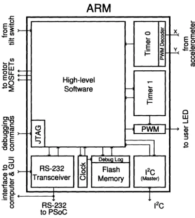
Each module contains two microprocessors that perform different tasks. The primary microprocessor is a 32-bit ARM processor produced by Philips. It is responsible for all of the high-level disassembly algorithms. The second processor is an 8-bit pro-grammable system on a chip (PSoC) that is manufactured by Cypress Microsystems. The PSoC handles the low-level functions that would otherwise occupy the ARM.
The two systems communicate using the I2C protocol [10].
3.1.1
Primary ARM Processor
The ARM processor executes all of the high-level algorithms that give the system the ability to self-disassemble. The processor, a Philips LPC2106, boasts a 32-bit wide data path, 128KB of reprogrammable flash memory for program storage, and 64KB of RAM for temporary data storage. We operate the processor at 11.0592MHz to minimize the ARM's power consumption, but the chip is capable of running at up to 60MHz [11].
A block diagram of the major hardware components of the ARM processor is displayed in Figure 3-3. Most of the functionality of the ARM chip is implemented in software and will be discussed in later chapters. Starting at the upper right portion of the diagram in Figure 3-3, the first hardware component worth noting is Timer 0. This timer interfaces with the accelerometer that is detailed in Section 3.4 and converts its two pulse width modified (PWM) output signals into acceleration estimates.
The next piece of hardware, Timer 1, operates as an interrupt source. It sends interrupt events to the software at fixed intervals. These interrupts serve two pur-poses. First, the interrupts, along with the PWM generator shown in the diagram, change the mode of the user LED so that it can display complex patterns that com-municate the state of the module to an observer. Additionally, the interrupts prompt
E CO CO,, OLH EcU
oO
.-E .E CD0 -00 5 0,0aoz CO--S: EARM
L_ a)Eo
a)00 CO o -J a) CD 08
RS-232 12C to PSoCFigure 3-3: The ARM processor contains numerous hardware resources which are crucial to the correct operation of the system. These resources are all controlled by the software which executes on the ARM.
the RS-232 transceiver, shown in the bottom left of Figure 3-3, to automatically re-transmit any messages that it has queued. The RS-232 transceiver is used by the modules to communicate with their neighbors. Any message destined for a neighbor is transmitted on this interface to the PSoC. The PSoC then routes the message to the appropriate neighbor. Details of the message format are covered in Chapter 4.
The RS-232 transceiver also communicates with a desktop computer over what we term the up-link interface. The up-link interface allows one module to serve as a bridge between a desktop computer and the distributed system. By connecting the system to a desktop computer, the user can easily visualize and sculpt the system using a graphical user interface (GUI). Once the user has modeled the cubes into a final configuration, the configuration is transmitted by the desktop computer over the RS-232 interface back to the system.
In addition to the RS-232 transceiver, the ARM has two other communication interfaces. The first is the I2C bus that it uses to interface with the PSoC. The ARM acts as the master of the bus and transmits requests to the PSoC. The PSoC then replies with the desired data. The final communication interface is the JTAG port, which can be used to debug the processor while software is being developed. The JTAG port allows the software developer to single-step through the source code, and, additionally, it also update the ARM's flash memory.
The last major piece of hardware on the ARM is the flash memory. One 8KB sector is reserved for use as a debugging log. If the ARM chip encounters errors during its normal course of execution, it logs them in this section of the memory. Then, even after the module has been power-cycled, the user can use the RS-232 interface to examine the contents of the log in an attempt to determine the source of any problems. All data stored in the log can be time-stamped with a resolution of one second using the clock which is illusrtated to the left of the debugging log in Figure 3-3 Time-stamping allows the user to reconstruct a composite sequence of events from event logs recorded in several different modules.
3.1.2
Secondary PSoC Processor
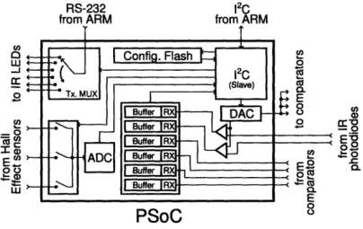
In addition to the ARM processor, each module in the system contains a Cypress CY8C29466 PSoC. Each PSoC has an 8-bit wide data path, 32KB of flash memory for program storage, and 2KB or RAM for data storage [9]. The PSoC is clocked by the same 11.0592MHz source as the ARM processor. The most significant benefit of using the PSoC chip is that it contains 32 reconfigurable hardware blocks that can serve many purposes. In particular, the CY8C29466 has 16 digital hardware blocks, eight of which are specifically designed for digital communication. It also contains 16 flexible analog blocks that lend themselves to processing and generating analog signals. Like the ARM, the PSoC can be reprogrammed without being removed from the circuit. Unfortunately, it cannot be debugged this way [9].
Figure 3-4 shows how we have configured the PSoC. The feature that is the basis for all of the PSoC's functionality is the I2C slave interface shown in the upper right-hand corner of the diagram. It continuously waits for commands from the ARM. When it receives a command, it processes or generates the provided or requested data, and, if required, transmits a response to the ARM. The I2C interface provides a means to control all of the PSoC's other peripherals.
RS-232 12C
from ARM from ARM
LU U, -) E 42 201.9o w mo E13 I.U U) CD (D __.-0 E0
00
oo a- .• .4PSoC
°
Figure 3-4: The PSoC processor implements much of the low-level functionality of the system. It is primarily responisble for buffering the data received from a module's six faces. The PSoC is controlled by the ARM processor using the I2C interface.
Moving to the left across the top of Figure 3-4, the next important hardware resource is the configuration flash. This 64-byte sector of the PSoC's non-volatile flash memory is used by the module to store configuration parameters that must be retained when the power is switched off. This sector contains information such as the module's unique identification number and several threshold values, which ensure that the communication and orientation detection systems operate correctly.
Next, in the upper left-hand corner of the figure, two of the PSoC's digital blocks are used to implement a 1-input, 6-output multiplexer labeled, "Tx. MUX." This
multiplexer, controlled by commands sent from the ARM processor over the 12C
interface, redirects the RS-232 data stream, (also generated by the ARM), to a specific IR LED on any of the six faces. By switching the output of the multiplexer, the ARM can send inter-module messages to a specific neighbor without also addressing all others.
Below the RS-232 multiplexer, Figure 3-4 illustrates the PSoC's analog-to-digital conversion subsystem. It is composed of two of the PSoC's analog blocks. The first part of the system uses a demultiplexer to select between three analog inputs: one from each of the Hall Effect sensors used in the connection mechanism described in Section 3.2. The single analog output of the demultiplexer is then routed to the analog-to-digital converter (ADC) to be processed. The ADC provides an 8-bit
digital output that ranges from 0 to 255 and which is routed back to the 12C block.
Moving to the right along the bottom of Figure 3-4, the next component is the RS-232 receiver. This block consists of six identical subsystems that first receive and decode RS-232 data stream and then buffer the received data. Each RS-232 receiver occupies one of the PSoC's digital communication blocks. Because the receivers are implemented in hardware, they can all operate in parallel. This ability allows a mod-ule to simultaneously receive messages from each of its six neighbors. Because the modules in the system do not transmit their messages in a synchronized pattern, it is important that a single module be able to handle messages from all of its neigh-bors concurrently. The buffers, which sit behind the RS-232 receivers, each have a capacity of 65 bytes-large enough to hold even the longest inter-module messages.
Additionally, the RS-232 receivers automatically detect the start and stop indicators transmitted with each inter-module message. When a complete message is received, the corresponding buffer will not accept any additional characters until it is explicitly flushed. This restriction guarantees that when the ARM queries any of the receive buffers using the I2C interface, the ARM always finds an empty buffer or a complete message.
Finally, the bottom right-hand corner of the PSoC block diagram in Figure 3-4 illustrates the digital-to-analog converter (DAC) and two of the comparators that are necessary for inter-module communication. In addition to the two comparators inside of the PSoC, there are four additional comparators in a separate integrated circuit. Together, the six comparators process the analog voltages returned from the six IR photodiodes on the module faces. The comparators' outputs are digital logic levels that can be processed by the RS-232 receivers. By modifying the analog voltage produced by the DAC, we can control the sensitivity of the receivers. Section 3.3 details the infrared communication interface.
3.2
Connection Mechanism
Individual modules bind to each other using switchable permanent magnet assemblies, hereafter referred to as Magswitches. These assemblies are produced by Magswitch Technology, Inc., and one is shown in Figure 3-5. Three faces of each cube contain Magswitches. Like all other components, they are mounted on the inside of the cubes and pass through similarly sized holes in the printed circuit boards. The other three cube faces are covered by steel plates. The steel is cold rolled A336/1008 that is 0.033 inches thick. When multiple cubes are assembled into a structure, Magswitches always attach to their neighboring cubes' steel plates, not other Magswitches. As a result, the modules can only attract one another. They do not repel but, instead, depend upon gravity or user intervention to clear unused modules from any final structure. A single Magswitch connected to a neighbor's steel plate can support over 4.5 lbs.-the combined weight of 17 other modules.
rotating
permanent
-magnet
- keyway
Magswitch body
Figure 3-5: Each Magswitch consists of a two permanent magnets stacked on top of each other inside of metal housing. The bottom magnet is fixed while the top one
contains a keyway and is free to rotate. As the top magnet is rotated through 1800,
the entire device switches from on to off or vice versa.
The Magswitch assemblies control a magnetic field by changing the relative ori-entation of two permanent disc magnets. The magnet with the keyway shown in the assembly in Figure 3-5 can rotate freely with respect to the fixed magnet that sits below it in the structure. Depending on their relative orientations, the Magswitch is either activated and attracts other ferromagnetic materials, or it is deactivated and releases it hold. The advantage of such a system is that power is only consumed while changing the state of the Magswitch. Once a Magswitch is on or off, it remains in that state indefinitely. This is invaluable for the battery life of the modules.
A miniature pager motor with an integrated gear box drives each Magswitch. These motors have stall torque of 0.28oz-in [12]. A 17-thread-per-inch worm gear is glued to the motor's output shaft. This worm gear turns a 30-tooth spur gear which has a key that matches the keyway of the Magswitch shown in Figure 3-5. The entire motor, worm gear, spur gear, and Magswitch assembly is illustrated in Figure 3-6. When driven with 4.1V, the voltage of a fresh lithium-polymer battery, the motor requires approximately 1.3 seconds to switch a deactivated Magswitch on and back off again.
The motor driver circuit consists of a single MOSFET. As a result, the motor can only turn in one direction, but three additional MOSFETs, which would be needed to run the motor in both directions, are eliminated. The drawback to such
motor pur gear ffect sensor top cove
Figure 3-6: A worm gear attached to the output shaft of a minature DC motor turns a spur gear that mates with the keyway in the Magswitch. In the figure, the Magswitch is obscured by the spur gear, and the temporarily removed top cover of the entire assembly is shown on the left.
a configuration is that if the Magswitch is not completely deactivated, the process of rotating it to the off position may momentarily turn it on. Additionally, the Magswitches become difficult to activate if they are not placed in contact with the steel plate on a neighboring cube. Because without a steel plate to complete the magnetic circuit, the magnetic flux must flow through an air gap which has a high magnetic resistance. This magnetic resistance translates into mechanical resistance which the motor sometimes fails to overcome. As a result, there is no guarantee that a Magswitch can be deactivated if it is not in contact with another cube. This restriction, while inconvenient for testing, does not affect the capabilities of the system as a whole because the Magswitches only need to deactivate when they are already in contact with other cubes.
A Hall Effect sensor is used to detect the state of each Magswitch. The Hall Effect sensor is placed such that its axis of sensitivity is aligned with the magnetic field produced by the Magswitch. This is shown in Figure 3-7. The Hall Effect sensor produces an analog voltage that is proportional to the attractive force produced by the Magswitch. An analog to digital converter in the PSoC microprocessor converts this analog voltage to an 8-bit digital value that ranges between 0 and 255. Figure 3-8 shows how the converter's output approximates a sine wave as the Magswitch is rotated continuously. We chose to orient the Hall Effect sensor such that the peaks in the plot correspond to times at which the Magswitch is fully activated, and the
minimums correspond to times when the Magswitch is completely off. Chapter 4 will discuss the algorithm that uses the Hall Effect sensor values to control the Magswitch's state. Hall Effect -sensor Magswitch body motor Eixed permanent nagnet gear
Figure 3-7: A Hall Effect sensor placed near the Magswitch is used to sense the amount of force it generates. We have chosen to align the Hall Effect sensor and Magswitch such that higher voltages at the output of the Hall Effect sensor correspond to stronger a attractive force.
3.3
Communication Interface
All communication between modules is performed using infrared light. Each of the six cube faces contains an infrared LED and an infrared sensitive photodiode. Together, these allow bidirectional communication between neighboring cubes at 9600 bits per second (bps). While higher bit rates were achievable, 9600bps proved adequate.
Infrared communication has several advantages over other alternatives such as direct electrical contacts. First, an infrared based system does not require that the faces of neighboring cubes be completely flush. In an assembly of many modules, this is a legitimate concern because imperfections in the manufacturing process produce cubes that are not perfectly square nor exactly the same size. Electrical contacts are also disadvantageous because they may short out on the steel plates that cover three of the six cube faces.
Hall Effect Sensor Voltage vs. Time Gý I 0 W 0 0 O C Cr Time [sec]
Figure 3-8: The output of the analog-to-digital converter connected to a Hall Effect sensor approximates a sine wave as the corresponding Magswitch is rotated con-tinuously. The Hall Effect sensor and Magswitch are oriented such that peaks in the converter's output indicate that the Magswitch is exerting its maximum holding force. The minimums in the plot correspond to times at which the Magswitch was deactivated.
the modules, the infrared LED and photodiode were not always placed in the center of each face. This decision dictates that every module have only one valid orientation in a composite structure if the LEDs and photodiodes of neighboring cubes are to align. However, because any multi-module structure must be assembled by hand, this restriction does not affect the functionality of the system.
The infrared LED and photodiode have both a limited range and a limited field of view. Like all of the electrical components, the LED and photodiode are mounted on the inside faces of the modules, and they point down through holes in the circuit boards. In order to prevent these holes from further restricting the field of view of the emitters or receivers, they are countersunk on the back (bottom) side of the boards. Figure 3-9 shows how the voltage at the output of the photodiode varies with dis-tance between the photodiode and the infrared LED if they are laterally aligned. It illustrates that two cubes must be immediate neighbors in order to communicate. It is not possible for two cubes separated by the width of another cube to communicate. Figure 3-10 shows how the voltage varies with alignment offset between the emitter and detector if two modules have their faces touching. To convert these analog volt-ages to digital signals that can be used by a microprocessor, a voltage comparator is used. It forces any input voltage above a threshold to 3.3V and any voltage below that threshold to OV. Empirically, a threshold voltage of 2.1V provided the best com-promise between robustness to misalignment and noise rejection. Higher thresholds tended to produce noisy output, and lower thresholds reduced the system's robust-ness to misalignment. The chosen 2.1V threshold allows two modules to communicate if they were placed within approximately 0.25 inches of each other. The threshold voltage is stored in the PSoC's flash memory, and it is simple for the user to change using the ARM's RS-232 interface if desired.
3.4
Orientation Detector
Each module is able to detect its absolute three-dimensional orientation by using a two-axis accelerometer and a binary tilt switch that are connected to the ARM
Photodiode Output Voltage vs. Distance •o 0 0 n 0. 0, 0 0 0.5 1
Distance Between IR LED/Phototransistor Pair [inches]
Figure 3-9: The voltage at the output of the photodiode varies as the IR LED is moved farther away. When the LED is off, the IR photodiode produces 3.3V. When the LED is turned on, the voltage produced by the photodiode drops by an amount inversely proportional to the distance.
3.5 3 S2.5 S2 a-S1.5 7, > 0.5 0
Photodiode Output Voltage vs. Offset
0 0.02 0.04 0.06 0.08 0.1 0.12 0.14 0.16 0.18 Offset Between IR LED/Phototransistor Pair [inches]
Figure 3-10: The voltage change at the output of the IR photodiode varies as the misalignment with the IR LED increases. In this test, two modules were placed face to face, and their alignment offset was gradually increased. When the LED is off, the IR photodiode produces 3.3V. When the LED is turned on, the voltage produced by the photodiode drops by an amount inversely proportional to the alignment offset.
microprocessor. The accelerometer returns two PWM signals that correspond to the acceleration that each axis is experiencing. The period of these signals is fixed, but the percentage of one period that the signal is on is proportional to acceleration. The ARM microprocessor measures the pulse width of the two signals to obtain an estimate of the cube's orientation.
The specific accelerometer, the MXD2004AL, produced by Memsic, Inc., was cho-sen because it is highly resistant to the large accelerations that can result from being
dropped []. Given a structure of modules that is disassembling, many of the unused
modules will detach and fall away from the structure. The accelerometer should be able to survive these falls.
A tilt switch is needed in addition to the accelerometer in order to detect a mod-ule's orientation when neither of the two accelerometer axes is experiencing accel-eration due to gravity. There are two possible orientations which produce such a situation. The tilt switch differentiates between these two configurations by turning on or off. Like the accelerometer, the tilt switch was chosen for its durability. Instead of a typical mercury-filled glass cylinder, each tilt switch uses a small metal ball bear-ing encased in a metal cylinder. While the tilt switch only tells the microprocessor whether the module is oriented roughly up or down, this information, combined with the more precise data from the accelerometer, is enough to determine which side of a module is facing down.
3.5
Power Regulators
Each module is equipped with two rechargable lithium-polymer batteries connected in parallel. These batteries supply power to the module's electronics and motors. They provide 3.7V nominally and have a combined capacity of 340mAh. If the batteries are fully charged and the module is continuously transmitting messages on each face but not running its motors, the useable battery life is over six hours. The batteries drive the motors directly, but two voltage regulators provide power for the electronics. One produces 3.3V which is used by all of the components. The other regulator
produces 1.8V which is only used by the core of the ARM microprocessor. The voltage regulators were chosen for their low-dropout voltages. The 3.3V regulator stops operating only when the batteries produce less than 3.5V [3]. Likewise, the
1.8V regulator drops out when the batteries can only supply 2V [4].
The modules can be recharged without removing the batteries. Each module contains an integrated circuit that manages the process. The electrical connection to recharge the batteries is provided through two of the metal faces that adorn the outside of the cubes. Large areas of solder mask are missing on the bottom (outside) of two of the printed circuit boards that form the faces of the cubes in order to electrically connect the steel plates to the circuit. To achieve a reliable connection, the plates are affixed with conductive epoxy. To recharge the batteries, the modules are set in a 28 inch long trough whose metal sides supply a potential difference of 5V. Because the trough is so long, it can recharge 15 modules simultaneously. Current to recharge each module's batteries flows from the sides of the trough, through the metal faces and conductive epoxy to the solder mask-free contacts on the back of the printed circuit boards. The integrated circuit responsible for managing the charging process automatically detects when a charging voltage is present. Therefore, starting or stopping the charging process is achieved by simply placing the modules in or removing the modules from the charging trough.
Chapter 4
Low-Level Software
To support the algorithms that allow our system of modules to disassemble, we have implemented a series of low-level functions that control the hardware in each module. These routines place an abstraction barrier between the localization, shape distribu-tion, and disassembly algorithms and the complex hardware contained in each module. This separation facilitates the rapid implementation and modification of the high-level concepts which are responsible for the system's visible behavior. The high-high-level algorithms do not have to contend with the specifics of basic tasks such as exchanging messages or activating a Magswitch.
Once a module has the ability to transmit and receive messages, the low-level operation reduces to the simple process illustrated in Figure 4-1. After initializing, a module loops forever, simply receiving and transmitting messages to its neighbors. The interesting behavior responsible for the system's self-disassembly is governed by how the high-level algorithms, described in Chapters 5 and 6, respond to received messages.
Section 4.1 of this chapter explains how the ARM and PSoC processors com-municate. Their cooperation is essential to all other functionality displayed by the modules. Both the ARM and PSoC are necessary to actuate the Magswitches, send messages, or receive messages from a module's neighbors. Section 4.2 presents the
algorithm used by the ARM processor to control the Magswitches using Hall Effect sensors.
Figure 4-1: The message processing loop executing on each module is simple. First, modules initialize all their peripherals. Then, they loop infinitely, receiving and sending inter-module messages. How a module changes its internal state in response to received messages and what messages it transmits in return, dictate the system's high-level abilities.
Sections 4.3 and 4.4 explain the process a module must follow in order to send and receive messages, respectively. In addition to explaining how messages are trans-mitted, Section 4.3 details the basic structure of all inter-module messages. Finally, Section 4.5 examines several specific inter-module messages and the actions that their reception prompts.
4.1
I2C Communication
The I2C bus protocol is based on the concept of a master and a slave. The master transmits requests to the slave, and the slave replies [10]. We have designed our disassembling system so that the ARM microprocessor is the master and the PSoC is the slave. This relationship allows the ARM to be in control of the bus and request data from the PSoC when necessary. The ARM may initiate two types of data transfers: write and read. Writing and reading data cannot be combined in a single I2C transaction. As a result, if the ARM wants specific data from the PSoC,
it must utilize a write transaction to inform the PSoC what data it wants before it executes the read operation. While the I2C specification allows for data rates of up to 3.4Mb/sec [10], we found that data rates above 20Kb/sec were unreliable given our choice of hardware. In large part, we feel this is due to the inability of the PSoC to simultaneously process the RS-232 data from the module's six neighbors and the
12C commands from the ARM.
Each I2C exchange, regardless of whether the ARM is transmitting or receiving, begins with the ARM sending one byte of data that contains the 7-bit I2C address of the PSoC (64) and one bit that indicates whether the ARM wishes to read or write data. If the ARM is writing data, the second byte of the I2C transmission is a command byte that indicates what type of data, if any, is to follow. Some commands transmitted by the ARM are followed by additional data bytes which further specify how the PSoC should react. If the ARM is receiving data from the PSoC, the PSoC should already know what type of data to provide, and every byte in the transaction after the first is sent by the PSoC to the ARM.
4.1.1
I2C Commands
Table 4.1.1 provides a list of valid I2C commands, the number of data bytes that are to follow, and an indication of whether they prepare the PSoC for a subsequent read transaction. For example, consider the first command listed in the Table 4.1.1, MONITOR HALL SENSOR. If the ARM wishes to read the current value of one of the Hall Effect sensors, it must first transmit a MONITOR HALL SENSOR command followed by one byte which specifies which Hall Effect sensor to monitor. After the 12C write is complete, the ARM initiates a read operation to which the PSoC replies with one byte containing the most recent output of the ADC connected to the specified Hall Effect sensor.
The STOP ADC command is closely related to the MONITOR HALL SENSOR com-mand. It is issued by the ARM whenever it realizes that it will not need to change the state of any Magswitches for a significant period of time. Because each Magswitch is actuated at most twice during any assembly/disassembly sequence, such times are
Table 4.1: The commands transmitted from the ARM to the PSoC over the I2C bus may be one byte long, or they may be followed by several parameters as specified by the Bytes to Follow column. Some commands, as denoted by the Read Next column, also prepare the PSoC to respond to request to read data.
PC Command Bytes to Follow Read Next
MONITOR HALL SENSOR 1 Yes
STOP ADC 0 No
SET TX CHANNEL 1 No
SET COMPARATOR 1 No
GET RX STATUS 0 Yes
READ RX BUFFER 1 Yes
SAVE CFG DATA 64 No
READ CFG DATA 0 Yes
common. When the PSoC receives the STOP ADC command, it turns its ADC off to conserve power until another MONITOR HALL SENSOR command is received. There is no additional data sent along with the STOP ADC command.
Other commands operate in similar fashion to the two already discussed. The SET TX CHANNEL command is used to control the digital multiplexer which redirects the RS-232 data stream generated by the ARM to an IR LED on any of the six faces. The additional byte expected after the initial command specifies the face to which the stream should be redirected.
The SET COMPARATOR, GET RX STATUS, and READ RX BUFFER commands control the flow of inter-module messages received from a module's six neighbors. In partic-ular, the SET COMPARATOR command modifies the output of the DAC, which drives the non-inverting inputs of the comparators used for processing the outputs of the six photodiodes. In this case, the additional byte transmitted by the ARM after the initial command specifies the output value of the converter. This, in turn, sets the threshold of the comparators. The GET RX STATUS command is used by the ARM to check which of the six RS-232 receive buffers have messages pending. The command requires no additional argument, but like the MONITOR HALL SENSOR command, read-ies the PSoC for a read operation in which it transmits a single byte which indicates which of the six receive buffers is full. After determining which of the six buffers
contains a pending message using the GET RX STATUS command, the ARM typically issues several READ RX BUFFER commands to read the contents of every buffer that contains a pending message. The additional byte sent after the READ RX BUFFER command specifies which buffer the PSoC should prepare to transmit back to the ARM. A subsequent 12C read retrieves that buffer contents.
Finally, the SAVE CFG DATA and READ CFG DATA commands provide a means for the ARM to store and retrieve configuration data from a single 64-byte page of the PSoC's flash memory. The SAVE CFG DATA command can be followed by up to 64 bytes of data to be stored. Likewise, the READ CFG DATA command prepares the the PSoC to return those 64 bytes during the next I2C read operation.
4.2
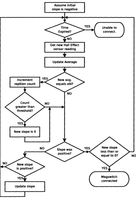
Magswitch Control
This section describes how feedback from a Hall Effect sensor and the ability to only turn a Magswitch in one direction, it is possible to precisely control the state of each Magswitch. As shown in Figure 3-8, the voltage produced by the Hall Effect sensor approximates a sine wave as the Magswitch is rotated continuously. We have oriented the Magswitches and Hall Effect sensors such that when the voltage produced by the Hall Effect sensor is at a minimum, the Magswitch is deactivated. Likewise, when the voltage is maximized, the Magswitch exerts its maximum holding force.
Due to variations in the assembly process, not all of the Hall Effect sensors are placed at exactly the same distance from the side of the Magswitches. This results in a variance in the minimum and maximum voltage produced by each sensor. As illustrated by the red data points in Figure 4-2, the variance is significant when the Magswitches are activated but not in contact with a neighbor's steel plate.
4.2.1
Threshold-Based Magswitch Control
Initially, we attempted to control the state of the Magswitches using threshold-based algorithm. We assumed that if the reading from the Hall Effect sensor was above a certain value, the Magswitch was activated. If the value was below a different