Confinement Effects on Multiexciton Dynamics
in Semiconductor Nanocrystals
MASSACHUSETTSINSTITUTE OF TECHNOLOGY by0
Katherine E. Shulenberger
L
BRARES
B. A. Chemistry Wellesley College, 2014
Submitted to the Department of Chemistry
in partial fulfillment of the requirements for the degree of Doctor of Philosophy
at the
MASSACHUSETTS INSTITUTE OF TECHNOLOGY
September 2019
© Massachusetts Institute of Technology 2019. All rights reserved.
Author...S
ig n a tu re re d a cte d
Department of 4 emistryAugust 14, 2019
Certified by ...
S ig n a tu re re d a cte d
...
Moungi G. Bawendi Lester Wolfe Professor of Chemistry ThesisSapervisor
Signature redacted
A ccepted b y ... Robert W. Field Haslam and Dewey Professor of Chemistry Chairman, Department Committee on Graduate Students
This doctoral thesis has been examined by a Committee of the Department of Chemistry as follows:
Signature redacted
Professor Gabriela Schlau-Cohen...
Chairman, 'Kesis Committee Assistant Professor of Chemistry
Professor Moungi G. Bawendi...
Professor William A. Tisdale...
Signature redacted
Thesis Supervisor Lester Wolfe Professor of ChemistrySignature redacted
Member, Thesis Committee ARCO Career Development Professor of Chemical EngineeringConfinement Effects on Multiexciton Dynamics
in Semiconductor Nanocrystals
by
Katherine E. Shulenberger
Submitted to the Department of Chemistry on August 14, 2019, in partial fulfillment of the
requirements for the degree of Doctor of Philosophy in Chemistry Abstract
Colloidal semiconductor nanocrystals are a promising platform for a number of technological developments in a wide variety of lighting applications. They also are an
incredibly useful model system to interrogate fundamental carrier interactions in crystalline semiconductor lattices. This thesis investigates the properties of multiexciton states in
semiconductor nanocrystals to build an understanding of what drives their emission dynamics and efficiency. A complete understanding of the processes which dominate in a wide variety of nanocrystal systems sheds light on electron-hole and exciton-exciton interactions and provides guidance on how to engineer nanocrystals for particular applications.
In the first two chapters, I will build a foundation of understanding of semiconductor nanocrystal systems, and how to build up an intuitive understanding of the states in question from both fundamental modeling and chemical intuition. I also present a variety of methods which are used to interrogate the luminescent properties of these materials, with a particular
focus on those utilized in this thesis. In the second chapter in particular, I focus on how
photoluminescence measurements can go astray, how to identify artifacts or background signal which could bias or invalidate data, and how to eliminate these artifacts.
The next chapter details the biexciton and triexciton emission dynamics and efficiency in CdSe nanocrystals. Utilizing a well-established and well-studied semiconductor systems allows nuanced interpretation of the emission dynamics, and the identification of perhaps some
unexpected material properties to enhance how we imagine these highly excited states. Chapter four employs a suite of methods to begin to understand carrier-carrier
interactions in cesium lead halide perovskite nanocrystals. This system provides a particularly interesting platform to investigate the effect of confinement and lattice mobility on excitonic properties.
Finally, I present a few experimental directions and ideas which have not yet been explored and would provide an excellent continuation of this work.
Thesis Supervisor: Moungi G. Bawendi Title: Lester Wolfe Professor of Chemistry
1 Acknowledgements
Looking back, it is truly a monumental task to try to thank all the individuals who have provided the opportunities, encouragement, and support that have brought me to this point in my life. Nonetheless, the following represents my best effort to put into words my gratitude for everyone who has been a part of my journey:
First, I want to thank my advisor Moungi Bawendi. I cannot describe just how much I have learned and grown through being a member of the Bawendi Group. Thank you Moungi for always encouraging me to follow the projects that excited me, teaching me the importance of careful rigorous experimentation, and providing me with the opportunities to improve myself as a scientist, a mentor, a teacher, and a person.
I also would like to thank Will Tisdale. Words are insufficient to express how crucial being a
part of the Tisdale group has been for my graduate work. Will, thank you so very much for welcoming me into your group, being a second advisor and mentor to me, and encouraging and fostering some of the most productive and exciting collaborations of my graduate career.
I would like to thank my thesis chair, Gabriela Schlau-Cohen for being an incredible resource
both for my personal and career development, as well as always being willing to discuss technical details as I built my microscope, and designed analysis software. I have also been incredibly fortunate to have had a series of truly excellent mentors and advisors throughout my entire academic career who have fostered my love of science and math and always encouraged me to pursue what I love: Chris Arumainayagam, Mala Radhakrishnan, Nolan Flynn, Carla Verschoor, Karen Atkinson, Ms. Eaton, Mr. Edun, Mr. Changaris, and Mrs. Miles. In particular, thank you to Professor A., who saw in a first-semester, first-year college student something and taught that baby academic to be a scientist, ask questions, find ways to answer them, that math really can explain the universe, and that is the most beautiful truth in this universe. We may now disagree what the most beautiful and important equation is, but I still look up to and aspire to be the kind of mentor youareone day.Thank you.
It is important to have not only supervisors and mentors who inspire you, but colleagues and collaborators too. In this, I have also been incredibly lucky. I know that through working with others my own projects have become more than they ever could have been had I been going it along. To Hendrik Utzat, we started this crazyjourney as first years with a blank slate, full of ideas and dreams. Through it all you have been an incredible scientific partner, and I appreciate how much you have pushed me to be excellent. To Matt Ashner, I can only say that you inspired me when I was stuck and saw no direction to finding answers. We may never have satisfactorily answered that original question, but along the way we answered questions I didn't even know were there. Having someone to verbally process with was crucial, but I also am so thankful for your friendship day in and day out. To Nathan Klein, I may have adopted you as a mentee, but you quickly became so much more. Between enabling the project I had been dreaming of for literal years, helping me solve complex sets of differential equations over coffee, and just listening and believing me no matter what, your influence rings through the following pages more than you may
ever fully know. To Sophie Coppieters 't Wallant, you are the most driven and brilliant student I could have hoped to work with. I may have thrown the book of solid state physics at you on day one, but you took it all in stride and taught me so much about being a mentor. The triexciton project is as much yours as it is mine. I know you will do big things in this world, and that is the greatest reward I could imagine. To Thomas Bischof, thank you for teaching me everything about optics, photon counting, and multiexcitons. You are truly a fabulous mentor. To Lea Nienhaus, you showed me the kind of scientist I aspire to be. Thank you for your continued support. To Maksym Kovalenko, Franziska Krieg, and all my other collaborators, thank you for helping me find answers. I couldn't have done it without you. To the spectroscopy subgroup, thank you for the thoughtful and productive discussions. To the Tisdale lab, thank you for being the best coworkers. Between coffee hour, crossword puzzles, volleyball, and Jamborees you have made work fun.
I started my doctoral work with a whole cohort of crazy, nerdy hooligans. Everyone said we
wouldn't be friends beyond that first semester, and I am so so glad that they were wrong. Sam, Dan, Brian, Nathan, Helena, Alex, and Jay, it's been a wild ride and I am so glad we took it together. I know that the bonds forged in the grad lounge are forever, no matter where we live. Thank you for the adventures and the laughs. Nicole, you may have started as the "favorite first-year," but I am so thankful that you became one of the group and for your friendship every day. Julia, I didn't know I needed a friend like you in my life until you appeared, and now I can't imagine it any other way.
In my time on MIT campus, I have developed strong ties to so many other groups and individuals that I could in no way begin to name them all, so I just want to thank my EAB, GSC, and Thirsty Ear families. You have enriched my life beyond my wildest dreams. I couldn't have done this without you. I also have had the most amazing support from a number of MIT offices which I cannot imagine having made it here without. Thank you to the Chemistry Education office, in particular Jennifer Weisman; the VPR team, in particular Meg Chuhran; the OGE, in particular Suraiya Baluch; and Tessa McClain.
Outside of MIT, I have found the most amazing family at Wolf Creek Stables. I came looking for an athletic outlet for academic stress and you gave me a family. Thank you to Brianna and Brandi for being amazing partners this summer and sharing Merlin. You have brought me so many smiles and laughs. Thank you to Eugene for being my barn partner. It's been a lot of hours (many in a car), and I treasure that time and your friendship. Kellie, you taught me to fly and I will always be grateful for my wings. There are far too many more to mention by name, but I love you all and am proud to be a part of the Wolf Pack.
It takes something very special to be willing to live with someone working towards a PhD. I have been very lucky in my roommates these past five years. Thank you Troy, Patrick, Rachel, Rose, Munchkin, Dan, Brian, and Alex for making my home a home through all the stress and craziness. To Mollie and Emily, we may not have lived at the same address since college, but Roomies are for life. #Triple. Thank you so much for being more like family than I could have imagined and for sticking by me through everything. Alex, you may never have lived with me officially, but thank you to my honorary roommate. Your practicality and sense of humor have lit up some of my darkest days. Brian, you are so much more than a roommate or yearmate. From
Pancake Sunday to adventures atop mountains in Alaska, you have been an incredible source of support. Thank you for being my partner.
To my Mom and Dad, you have been with me every step of the way. From late night childhood science experiments to late night phone calls walking home I have always felt supported and encouraged. Thank you for believing in me and in my dreams and paving the roads for those dreams no matter where they led. Everything I am is because of you.
Finally, to Munchkin, my other half, my "little" sister. I knew the first time I laid eyes on you that you were the most important person in my world. I always knew you would grow into a woman
I could look up to (both literally and figuratively), but I am still wowed by you every day. No
matter the distance, I always know I can count on you and that has meant more than I can say. I cannot wait for all our adventures to come. Thank you.
Contents
I
Acknow ledgem ents ... 62 Introduction ... 14
2.1 Sem iconductors ... 15
2.2 Sem iconductor Nanocrystals ... 16
2.2.1 Exciton Dynam ics ... 17
2.2.2 Biexciton Dynam ics ... 20
2.3 M ethods ... 21
2.3.1 Ensem ble M ethods ... 22
2.3.2 Single Particle M ethods ... 24
2.3.3 Solution Correlation M ethods ... 30
3 Chapter Experimental Considerations for Photo luminescence Measurements ... 32
3.1 Photon Counting Detectors ... 32
3.1.1 SPA D ... 32 3.1.2 PM T ... 33 3.1.3 SN SPD ... 34 3.2 SPAD Artifacts ... 35 3.2.1 Instrument Response ... 35 3.2.2 Dead Time ... 36 3.2.3 Afterpulsing ... 38 3.2.4 Photon Em ission ... 39
3.2.5 Chrom atic Aberration ... 40
3.3 Background Signal ... 41
3.3.1 Dark Counts ... 41
3.3.2 Laser Leakage ... 42
3.3.3 Substrate and Solvent Em ission ... 42
4 Chapter M ultiexcitons in CdSe N anocrystals ... 54
4.1 Background ... 55
4.2 Biexciton Statistical Scaling ... 60
4.3 Triexciton Scaling ... 65
4.5 M ethods ... 79
5 Chapter M ultiexcitons in Perovskite N anocrystals... . 81
5.1 Background ... 82
5.2 Ensem ble Photo lum inescence ... . 83
5.3 Transient Absorption Measurement of the Biexciton Spectrum... 91
5.4 Fluorescence Interm ittency M echanism ... 102
5.5 Statistical Scaling ... 107
5.6 Conclusion... 114
5.7 M ethods... 115
6 Chapter Future W ork ... 118
6.1 Biexciton Binding Energy of a Single N anocrystal ... 118
6.2 Size-D ependent CdSe N anoplatelet Biexciton Dynam ics ... 121
6.3 Investigation of Shell Effect on Triexciton Recom bination... 123
List of Figures
Figure 2-1 Schematic of single particle fluorescence microscope... 24
Figure 2-2 Fluorescence intensity plots ... . 25
Figure 2-3 Single-molecule second-order correlation plot ... 28
Figure 2-4 Photon Number Resolved Lifetime (PNRL)... 28
Figure 3-1 Avalanche photodiode (APD) schematic... 33
Figure 3-2 Photomultiplier tube (PMT) and super conducting nanowire single photon detector (SN SP D ) schem atics ... 34
Figure 3-3 Instrum ent response of an APD. ... 36
Figure 3-4 Detector dead-tim e exam ple ... 37
Figure 3-5 D etector after-pulsing... . 39
Figure 3-6 D etector photon em ission... . 40
Figure 3-7 Lifetim e background subtraction. ... 46
Figure 3-8 Two photon lifetime and quantum yield background subtraction ... 46
Figure 3-9 Intensity drift in a solution biexciton quantum yield measurement... 51
Figure 4-1 Biexciton recombination pathway illustration ... 58
Figure 4-2 CdSe exciton lifetim e ... . 60
Figure 4-3 CdSe biexciton lifetime, quantum yield, and residual exciton lifetime ... 61
Figure 4-4 CdSe-CdS shell thickness series and biexciton recombination dynamics... 64
Figure 4-5 CdSe triexciton recombination dynamics. ... 65
Figure 4-6 CdSe-CdS single nanocrystal results ... 69
Figure 4-7 CdSe-CdS heterogeneity test with band-pass filter... 70
Figure 4-8 CdSe-CdS absorption cross section measurement via fluorescence lifetime... 71
Figure 4-9 CdSe-CdS high-flux emission spectra ... 72
Figure 4-10 CdSe-CdS triexciton emission branching ratio measurement... 73
Figure 4-11 TDDFT modeling of CdSe P-state lifetime ... 75
Figure 4-12 Particle in a box modeling of S-state and P-state wavefunction in CdSe-CdS... 77
Figure 5-1 CsPbBr3 nanocrystal characterization ... 83
Figure 5-2 Ensemble spectral properties with and without air exposure under high and low flux excitation of CsPbBr3 nanocrystals... . 85
Figure 5-3 Evidence for photo-induced sintering of CsPbBr3 nanocrystals ... 86
Figure 5-4 Further photoluminescence evidence for nanocrystal sintering... 87
Figure 5-5 Assignment of biexciton binding energy bound from photoluminescence data... 88
Figure 5-6 Additional TEMs of aggregated and sintered nanocrystals. ... 89
Figure 5-7 Raw DLS correlation curves ... 90
Figure 5-8 Characterization of CsPbBr3 nanocrystals for transient absorption studies... 92
Figure 5-9 Spectral evolution of transient absorption data over different delay times... 94
Figure 5-10 Three different regimes with different spectral content of transient absorption m easurem ent ... 95
Figure 5-11 Exciton and biexciton component spectra of CsPbBr3 nanocrytals... 99
Figure 5-13 Exciton single nanocrystal characterization of a single CsPbBr3nanocrystal... 104
Figure 5-14 Excitation wavelength dependent nanocrystal blinking... 106
Figure 5-15 CsPbBr3biexciton quantum yield and lifetime... 107
Figure 5-16 Blinking dependent biexciton lifetime and quantum yield ... 108
Figure 5-17 R esidual exciton lifetim e... 110
Figure 5-18 CsPbI3 single nanocrystal biexciton dynamics ... 113
Figure 6-1 Schematic for proposed biexciton binding energy measurement ... 118
List of Tables
Table 4-1 Possible electron and hole angular momentum states for band-edge carriers... 56
Table 4-2 One possible biexciton state and the relative angular momenta of the four carriers which com prise the state... 59
Table 4-3 Calculated overlap integrals for the S-state and P-state wavefunctions... 77 Table 5-1 Median parameters recovered from the MCMC ensembles... 97
Table 5-2 Exciton radiative lifetimes extracted from single NC data and solution biexciton quantum yield values used to predict the statistical scaling biexciton lifetime... 111 Table 5-3 Comparison of the expected biexciton lifetime from a statistical scaling model and the biexciton lifetim e extracted from the TA data... 112
2 Introduction
This thesis details the photophysical properties of colloidal semiconductor nanocrystals, also known as quantum dots, under device relevant conditions for lighting and lasing applications. Semiconductor nanocrystals (NCs) are technologically interesting fluorophores for these applications due to a number of reasons. First, they are colloidally stable, and therefore solution processable, allowing for integration into devices through spin coating,1,2 dropcasting,' 4 or ink-jet printing5-7 and are therefore compatible with flexible substrates. Next, due to quantum confinement of the exciton - a bound, correlated electron-hole pair - semiconductor NCs have tunable bandgaps simply by changing the NC size.8 9 Furthermore, in part due to highly optimized syntheses, many semiconductor NCs have narrow emission linewidths with negligible heterogeneous broadening.10'" Finally, highly developed semiconductor NC systems, such as CdSe, regularly have unity or nearly unity exciton quantum yield.10,12-14 That is to say, for every excitation created one photon is emitted. There is a small caveat here, however; while the single exciton state has unity quantum yield, NCs may sustain more than one excitation simultaneously and these multiexciton states have drastically lower emission efficiencies.15'16 Nonradiative recombination from multiexciton states may currently act as an energy loss mechanism, but the presence of these states also provides an opportunity to overcome lifetime-limited fluorescence saturation, a major drawback to the use of molecular dyes for high-flux emission
applications.'7-19 Thus, a thorough understanding of multiexciton states, the driving forces between radiative and
nonradiative processes, and how to control them is crucial in the optimization and continued commercialization of semiconductor nanocrystals. The following chapters set forth to establish the current understanding of these multiexcitonic states, the methods that exist to interrogate them,
and my work expanding both our methodology and understanding of multiexcitons in nanocrystalline semiconductor lattices.
2.1 Semiconductors
In order to fully understand the dynamic processes dominating NC systems, I begin by considering the energetic bands which determine the properties of bulk semiconductor materials. While nanocrystals exhibit properties that fall between those of molecular systems and bulk semiconductor materials, it is a cleaner mental exercise to discretize the bulk systems, rather than expand the discrete molecular picture to many thousand atoms.
There are many excellent works which detail how to calculate the band structure of a bulk semiconductor through a myriad of methods, each with specific strengths and drawbacks.20 For a qualitative understanding of band edge states, simple linear combination of atomic orbitals
(LCAO) approximations can be quite illuminating. Perspectives gained from LCAO theory, or in
the semiconductor world, tight-binding models, provide an excellent first approximation of semiconductor properties. Determining the atomic orbitals which dominate the behavior of the valence band maximum and conduction band minimum provide key insights into the angular momentum and degeneracy of those states.
In order to calculate full band structures, the results of k-p theory describe the energy states observed in bulk and nanocrystalline semiconductors quite well. k-p theory is a perturbation method where the Hamiltonian can be written in the form shown in equation (2-1).
p2 h2k2 hk -p
H =2+ V + + (2-1)
The Hamiltonian can be separated into the first two terms to form the unperturbed Hamiltonian, and the second two terms which are the perturbed Hamiltonian. The method gets its name for the dot product of the reciprocal space and momentum operators present in the fourth term above and is particularly adept at calculating electron and hole effective masses at and around the gamma point. This is because the smaller k, the more accurate the perturbation method is because the contribution from the perturbed Hamiltonian decreases.
As I have alluded to already, these energy states are not discrete states with well-defined energy and momenta but a continuous surface of energy states represented in reciprocal space. That is to say a given state can have a range of energy and momentum properties depending on the position within the lattice.
At room temperature, it is most accurate to discuss the properties of electrons and holes as quasi-independent in most bulk semiconductors. However, there is an attractive Coulomb interaction between the positively-charged hole and negatively-charged electron which results in a binding energy.21 Generally, this binding energy is sufficiently small compared to thermal energy that entropic driving forces result in the dissociation of electrons and holes. However, at low temperatures or in semiconductors with unusually high binding energies it is possible that the
electron and hole remain energetically bound. This bound state is referred to as an exciton.
2.2
Semiconductor Nanocrystals
The picture outlined above changes slightly when moving to nanostructured materials. These nanomaterials can come in many different morphologies such as nanospheres,8 nanocubes,9 nanoplatelets,22 nanorods,23 and exotic shapes such as tetrapods.2 4 Materials can be further modified by combining multiple semiconductors such as core-shell nanocrystals,2s dot-in-rod heterostructures, 12 Janus particles,26 as well as core-shell2 and core-crown28 nanoplatelets.
Starting with the core-only materials, the band structure changes drastically based on the finite size of the nanocrystal. One way to consider this is that the bands discussed in the bulk case are actually just the infinite possible linear combinations of atomic orbitals that can be formed with the quasi-infinite number of atoms in a bulk crystal. Each of these states is so close in energy to the next, they can be accurately depicted as a continuum of states. When moving to a nanoscopic system, rather than the infinite number of atoms we consider in the bulk phase, there are a finite number (tens to thousands) of atoms. The finite nature of the atomic composition results in a discretization of the band structure, particularly around the band-edge. We may still consider these states using the same atomic orbital compositional arguments which are used in the bulk-case to describe the angular momentum character and degeneracy, but these states now have finite occupancy. Furthermore, due to both the energetic and spatial confinement, the excited state is strongly excitonic, resulting in an increased absorption resonance near the band-edge and correlated electron-hole angular momenta. Since the electron and hole remain spatially correlated, the emission efficiency of semiconductors also increases drastically due to constant and high wavefunction overlap. In order to fully understand multiexciton dynamics within this energy landscape, we first must have a thorough understanding of the exciton state to use as a basis for comparison.
2.2.1 Exciton Dynamics
In a perfect world, a nanocrystal will emit at a constant intensity that is determined by the radiative rate of the emissive state and absorption probability at a given excitation fluence.29 In the real world, even individual emissive processes are limited by shot noise, or uncorrelated random events. Thus, emission from a single radiative state does not have a single intensity over time, but rather a distribution of intensities. These intensities fit to a Poisson distribution centered around a given average, which can be determined from the absorption cross section and excitation fluence.
The dynamics of a single radiative state will be a purely monoexponential decay with a rate equivalent to the intrinsic radiative rate of the given state.30 Intensity trajectories are rarely
comprised of emission from a single shot noise limited state though, and a number of competing processes must be taken into account.
Almost all nanocrystal systems demonstrate fluorescence intermittency, or blinking, behavior on millisecond to minute time scales, depending on the exact nanocrystal sample.31-3 4 This intermittency is due to changes in nanocrystal structure, ligand coverage, and charge state which leads to transient trap states as well as fluctuating trion (either a positively or negatively charged state) formation.3 133 Trion states are generally emissive, with a lower quantum yield than the neutral exciton due to the availability of nonradiative Auger recombination.35~37 An Auger process is the recombination of an electron with a single hole and rather than emitting the affiliated energy as a photon, promoting a third carrier (either an electron or hole) into a state deep in the conduction or valence band. That carrier then rapidly cools through phonon emission back to the band edge, resulting in the relaxation of an exciton without emitting a photon. It is highly likely that the positive and negative trion states will have different quantum yields due to differential Auger rates for each.36 Trion states are generally identifiable by their intermediate emission intensity which corresponds to a drastically quenched fluorescence lifetime.31 If the pure trion state can be isolated, it should still emit with monoexponential decay kinetics with a faster lifetime.36
Trap states often exhibit two distinct types of behavior dependent on their energy level and accessibility: those accessible from the band-edge, and those only accessible during hot carrier cooling.33 Trap states that are thermally accessible from the band edge will manifest as a changing emission intensity and lifetime. Depending on the energy and density of trap states, the effect on the lifetime will be variable. Traps that are only accessible during hot carrier cooling will result in
a decreased emission intensity, but no change to the emission dynamics. There are a number of thorough reviews of nanocrystal blinking behavior which detail the differences in these processes. In particular, Yuan, et al., 31 describes single nanocrystal blinking quite well, highlighting the difference between individual nanocrystals in a fairly homogeneous ensemble.
Almost all deviations from monoexponential behavior in ensemble fluorescence lifetimes can be attributed to either nanocrystal heterogeneity, transient charging, or trapping.2 9 ,31 Ensemble heterogeneity will manifest as multiexponential or stretched exponential behavior with many radiative rates which are all similar in time constant, and usually in some form of continuous distribution.38,39 Pure charging will manifest as a biexponential decay with one exponential component corresponding to excitonic recombination, and one component corresponding to the radiative and nonradiative rate for the trion state.36 Trapping is more likely to have strong multiexponential character, but unlike with ensemble heterogeneity, it will usually manifest as a rapid early time component characteristic of the trapping rate, and then longer time dominated by the intrinsic exciton lifetime.3 1 It is of course also possible to have contributions from any of these in combination.
It can be a challenge to isolate exciton behavior from that of trapping and charging processes even in a single NC measurement which eliminates heterogeneity. The most basic method to do so involves examining a histogram of fluorescence intermittency and selecting a cut-off intensity which separates the high-intensity, excitonic state from other lower efficiency states.29 This method is commonly referred to as thresholding and has the advantage of being straightforward. However, it has been demonstrated that the selection of an 'on' state threshold imposes a significant amount of user bias, particularly in rapidly fluctuating or complex intensity
trajectories. Change point algorithms are one of the main alternative methods to analyze this intermittency. 4 These methods are discussed in detail in Chapter 3.
The next crucial component in understanding exciton dynamics, once charging and trapping contributions have been identified, is a thorough picture of the exciton fine structure. Fine structure is discussed in detail in Chapter 4. When considering exciton dynamics the major contributions from nanocrystal fine structure are the total angular momentum of each state, which determines whether a state is emissive (bright) or non-emissive (dark), and the energy splitting between these states.
2.2.2 Biexciton Dynamics
Once a complete understanding of exciton dynamics has been established, multicarrier processes must then be considered. When studying a biexciton or higher excited state, not only are charge and trap states influencing the quantum yield and dynamics of the material, but multicarrier non-radiative processes are as well.' 44 Auger recombination is believed to be the dominant mechanism which results in multiexciton quantum yields which are less than the exciton quantum yield of a system, in addition being the mechanism for the reduced quantum yield of trion states discussed earlier.36 The Auger rate is determined by the electron hole wavefunction overlap and the density of final states available to the promoted carrier.46 The Auger rate in CdSe and CdSe/CdS nanocrystals have been extensively studied and for core-only materials almost universally scales with the volume of the NC.47 There have been a few more recent exceptions to
this universal volume scaling of Auger rates, such as in 2-D nanoplatelets.48
If Auger rates dominate the nonradiative processes for multiexciton states, then the next
crucial quantity to determine is the radiative rate. For any given state, the two most important factors in determining the radiative rate are the energy of the transition and wavefunction overlap. For the energy of the transition, from a first glance it should be the same as the energy of the
exciton. At minimum the band-edge of all semiconductor NCs have a degeneracy of two. Therefore, the biexciton occupies the same state and ignoring exciton-exciton interaction, will have the same energy. The difference between the energy of two isolated excitons and a biexciton is termed the biexciton binding energy.'6 The first order consideration of the biexciton binding energy would be the Coulomb interaction between the four carriers. The electron-hole interactions should directly cancel with the electron-electron and hole-hole interactions and thus there should be no expected binding energy. Taking higher-order Coulomb and Exchange interactions into account results in a small biexciton binding energy.4 9'50 In most core-only materials studied thus far, binding energies are on the order of a few meV and attractive in sign.5' Extensive
heterostructure engineering has succeeded in creating CdSe/CdS NCs with large repulsive biexciton interactions through carrier separation, demonstrating there is no guarantee that a biexciton interaction must be attractive.5 2
The next consideration is the wavefunction overlap, but since the exciton and biexciton must occupy the same states, there is unlikely to be much difference in the overlap, and therefore the radiative biexciton rate should not be appreciably different from the exciton, ignoring fine-structure considerations. The fine-fine-structure of a given state will determine the multiplicity of recombination pathways, and thus the scaling of the biexciton rate as compared to the exciton. This scaling is discussed extensively in Chapters 4 and 5.
Due to the complex nature of multiexciton emission processes, it is crucial to have nuanced methods to interrogate these dynamic processes. The following sections describe the methods utilized in this thesis.
This section details all the spectroscopic methods used throughout this work. The majority of data are collected through a variety of fluorescence techniques, but some absorption methods are also utilized. Fluorescence techniques include single nanocrystal confocal methods, ensemble-averaged single molecule methods, and wavelength dependent ensemble methods. The combination of these allows the nuanced interrogation of exciton and multiexciton dynamics towards the goal of understanding the dominant states and processes relevant for high-flux nanocrystal applications.
2.3.1 Ensemble Methods
2.3.1.1 Ensemble Photoluminescence Lifetime
The lifetime of any fluorescent sample is the decay curve of the emission process. When a sample is excited using a pulsed laser source, the entire fluorescent population is created simultaneously. By monitoring the delay between the laser excitation pulse and the detection of an emitted photon, then taking a histogram of the delay times, a fluorescence decay curve can be constructed. This method is generally referred to as Time-Correlated Single Photon Counting
(TCSPC).
2.3.1.2 Spectrally Resolved Photoluminescence Lifetime
There are two methods used in this thesis to spectrally resolve the photoluminescence lifetime. The first utilizes the same photon counting detector as a traditional PL lifetime measurement, but the detector is placed at the output of a monochromator. By sweeping the center wavelength across the fluorescence spectrum the lifetime can be measured at each spectral position. In a truly homogeneous sample that is emitting exclusively from a single state the lifetime at each spectral position will be identical. However, if a photoluminescence decay contains emission from multiple states or sample subpopulations, the dynamics will vary as a function of wavelength.
The other method used in this thesis to measure wavelength-dependent dynamics is a streak camera. In this case, rather than scanning a monochromator and only selecting one wavelength at a time, the spectrum is dispersed by a spectrograph. Then the collected light is converted to electrons by a photocathode and passes through a streak unit, which sweeps an increasing voltage as a function of time after laser excitation. The stronger the voltage, the more distance the detected signal is translated at any given time. Thus a streak camera spatially separates emission based on the time after excitation. The two-dimensional data (time and wavelength) is then imaged using a traditional CCD camera, producing a wavelength-dependent lifetime. One major advantage of a streak camera is that the time resolution is limited by the rate at which the voltage can be swept, and thus much higher temporal resolution can be achieved, unlike single-photon detectors. On the other hand, the lower sensitivity of CCD cameras results in this method only being applicable for fairly concentrated and highly emissive samples, whereas the single photon sensitivity of APDs allows for the detection of signal from an individual NC.
2.3.1.3 Transient Absorption Spectroscopy
In addition to the photoluminescence methods described above, this thesis also contains results from transient absorption (TA) spectroscopy. In brief, transient absorption is an ultrafast absorption method which can be used to interrogate the dynamics of occupied states after excitation, providing complementary information to photoluminescence results. PL can only interrogate states which couple to the rate of photon emission within a kinetic model. TA is an ultrafast pump-probe technique. First, a femtosecond pulse of monochromatic light is focused onto the sample. Usually this pump source is chosen to be well above the band edge. In this thesis a 400 nm pump source was used to excite the NC samples. After some delay, a broad-band probe pulse is also focused onto the sample. The absorption of the probe pulse is measured with and without the pump pulse through the use of a mechanical chopper, and the transmitted probe light is imaged
through a monochromator onto a CCD camera. The time delay between the pump and probe pulse is then varied through a stage delay which can scan up to -3 ns for the instrument used in this work.
2.3.2 Single Particle Methods
This thesis utilizes a large distribution of methods to analyze the dynamics and properties of light emitted from a single nanocrystal. All these methods are predicated on the same experimental setup, and also provide the dominant body of work for this thesis.
The microscope is a home-built single particle fluorescence instrument. There are a number of available excitation sources, all of which are fiber coupled into the microscope. Most data are collected using either a 405 nm or 532 nm pulsed diode laser as an excitation source. The excitation beam is directed through a series of neutral density filters which are used to control the incident laser power, then directed off a dichroic mirror into a microscope objective. For single-particle experiments an oil immersion objective is used, and for solution phase correlation measurements a water immersion objective is used. The microscope objective is mounted to a motorized unidirectional stage which can be used to bring the sample into focus. The sample is mounted to a three-axis piezo stage with sub-nanometer precision in x, y, and z. The z dimension is used to optimize the microscope focus, and the x and y directions are used to perform raster scans across the sample. Emission from a nanocrystal in the focal volume is collected by the same objective and separated from the excitation source using a dichroic mirror (either 425 nm long pass or 535
nm long pass). Emission is further filtered using a 1:1 telescoping pinhole (10 cm focal length
Sample 3 4
TCSPC
Pulsed
Excitation 1 2
Source e
8 x10- , , , 4000 7 a) v16 3000 4 ~2000 UO 3 2 1000-00 400 800 1200 1600 0 1 2 346 7 Time(s) Counts/Pulse x1
0-Figure 2-2 A fluorescence intensity trace with 40 ms time bins and the histogram of the intensity states. The low intensity state is shot noise limited. The high intensity state is not, predominantly due to microscope drift throughout the experiment.
achromat lenses, 50 pm pinhole) and additional emission filters (425 nm long pass or 532 nm notch). After filtering, the emission is split into four equivalent beams using three 50:50 beam splitters in the geometry shown in Figure 2-1. Each of the four beams is then focused onto a single photon counting detector using a 10 cm focal length lens. The turning mirrors in the detection component of the microscope are all cold mirrors (reflect < 700 nm and transmit >700 nm) to suppress detector crosstalk (discussed further in Chapter 3). Detection events are recorded using a HydraHarp 400 in t3 mode. These records note the pulse number after which a photon arrived, the time after the laser pulse, and the detector number at which it arrived for each photon. This record of photon arrival times will henceforth be referred to as the photon stream, and is the basis for the following single molecule analyses. In total the fluorescence setup described here is optimized for high detection efficiency, collecting roughly 15% of emitted photons in the green, with efficiencies peaking in the 600-700 nm range based on the efficiency of the detectors in that wavelength range. No photon detection can occur above 700 nm without further modifications due to the cold mirrors utilized in the detection component of the microscope. In order to reduce background counts, the entire microscope is enclosed in a homebuilt blackout box, and detectors are fitted with lens tubes
which eliminate almost all stray light. The following describe different analysis methods that can be applied to the photon stream after data collection.
2.3.2.1 Intensity Trace
An intensity trace may be generated from the photon stream by selecting a time window (say 5 ms), counting how many photons arrive in each 5 ms bin, and plotting these as a function of time. If a sample is constantly in a single emissive state, the spread of intensity values will be shot noise-limited and follow a Poisson distribution. There may be multiple discrete states which are shot noise-limited, or many many quasi-continuous states which do not fit any one distribution well. These distributions may be examined by taking a histogram of the intensity states as demonstrated in Figure 2-2.
2.3.2.2 Lifetime
The fluorescence lifetime of a sample is the histogram of delay times between an impulsive excitation event, and the detection of an emitted photon. The method is identical in theory to the ensemble lifetime described above, but instead of measuring the average behavior across many different nanocrystals, it measures the emission from an individual NC.
2.3.2.3 Biexciton Quantum Yield
This second order correlation method which can be used to extract the quantum yield of the biexciton state was derived in great detail by Nair et al.5 3 Rather than walking through the detailed mathematical justification for the method, which can be found in the supplemental information of Nair et al.,53 Figure 2-3 presents a qualitative understanding of why the center to side peak ratio measures the biexciton to exciton quantum yield ratio. The side peak represents events where a single photon was absorbed and emitted on two successive pulses. The center peak represents when two photons are absorbed and emitted after a single laser pulse. Due to the Poissonian absorption statistics of nanocrystals, the two absorption events described for the center
and side peak have equivalent probabilities. Thus, the ratio between the two peak areas is the ratio of quantum yields.
There are a few key conditions that must be met for the following explanation to hold though. First, the nanocrystal must be absorbing in the low flux regime. That is to say, it must be statistically likely that when one photon is detected, it originated as a single exciton. Similarly, when two photons are detected, they likely originated as a biexciton, etc. A good benchmark for the low flux criteria is <0.01 excitations per pulse. Next, the second photon of a biexciton must be exactly the same as an independently excited, single exciton. If the second photon of a biexciton does not have the same quantum yield as a single exciton, then some of the terms in the derivation do not appropriately cancel. Finally, the Poissonian absorption statistics that have been described for NC systems must hold, otherwise the absorption probabilities for the center and side peak scenarios will vary.
Assuming all these conditions are met, the center to side peak ratio then reduces to
Acenter QYBXQYX (2-2)
Excitation Emission 1200 Time 00 S800-Side T o400 Center C 0
I-800
-400 0 400 800 T (ns)Figure 2-3 Schematic of the second-order correlation measurement where the center peak (green) corresponds to two photons detected after the same laser pulse, and the side peak (blue) corresponds to two photons detected on subsequent laser pulses.
Where Acenter and Aside are the center and side peak areas respectively and QYBx and QYx are the biexciton and exciton quantum yields respectively. The numerator then corresponds to the quantum yield of the first and second photon of a biexciton, and the denominator corresponds to the quantum yield of two single excitons. Thus, the expression reduces to simply the biexciton to exciton quantum yield ratio. In the case where the exciton has 100% quantum yield, the center to side peak ratio is exactly the biexciton quantum yield.
2.3.2.4 Biexciton Lifetime
The biexciton lifetime can be extracted through low-flux, single-particle photon number counting methods as described by Shulenberger et al. By selecting only for pulses where two photons were detected after a single excitation pulse, the first detected photon then corresponds to
Time Excitation Emission Photon 0 1 2 Index -0 4 lt PNRL~zO-I PNRL Hf PNRL (,.2) ,0 40 Time (ns)80 120 160 200
Figure 2-4 Illustration of the various lifetimes extracted from two photons events and the notation used to describe these time delays.
emission from the biexciton state, and the second detected photon corresponds to emission from the residual exciton left behind after biexciton recombination. The biexciton lifetime is the histogram of time delays between the excitation pulse and the arrival of the first photon. The lifetime of the residual exciton is the histogram of time delays between the arrival of the first photon and second photon. Shulenberger et al.5 4 describe these photon number resolved lifetimes
(PNRLs) using the notation PNRLI2 ,, ) and PNRL(2,1,2> respectively, where the superscript notation
corresponds to the number of photons detected, the start index, and the stop index, as illustrated in Figure 2-4. There is a third lifetime which can be calculated from two photon detection events, PNRL 2 0 2, or the delay between the excitation pulse and the detection of the second photon. These
data contain information about both the biexciton and residual exciton lifetime together and are therefore generally not used.
2.3.2.5 Triexciton Quantum Yield
The triexciton quantum yield of a single particle is derived in the supplemental information of Shulenberger et al.54 Following in the methodology established by Nair et al.,53 the emission probability of three photons detected after a single excitation pulse is the product of the triexciton, biexciton, and exciton quantum yields. The equivalent to the two-photon side peak in the three photon experiment is two photons detected after a single laser pulse, with an emission efficiency that is the product of the biexciton and exciton quantum yields, and a single photon on the subsequent pulse with an emission efficiency of the single exciton quantum yield. Thus the ratio of the area of these two peaks is described by the relationship below.
QYTXQYBXQYX (2-3)
QYBXQYXQ YX
Where QYTx, QYBX, and QYx correspond to the triexciton, biexciton and exciton quantum yields
the ratio of the center and side peaks is the triexciton to exciton quantum yield ratio. It is crucial to note the analogous condition to the biexciton side peak is not three photons after three successive pulses, because it is necessary to cancel the biexciton quantum yield term from the center peak.
2.3.2.6 Triexciton Lifetime
The triexciton lifetime follows the same logic as the biexciton lifetime. First, the photon stream is sorted for all three photon detection events. Since experiments are run under low-flux conditions, these events correspond to almost exclusively triexciton emission. The lifetime of the triexciton is the histogram of delays between the laser pulse and first photon (PNRL(3 0 ,1 )), the residual biexciton lifetime is the histogram of delays between the first photon and second photon (PNRL' '12)), and the lifetime of the residual exciton is the delay between the second photon and
third photon (PNRLO 2
1). Extracting a lifetime from a fluorescence decay curve requires more total emission counts the longer the lifetime. Due to low total count rates, it is rare that the lifetime of the third photon of a triexciton has sufficient signal to noise to separate NC signal from the uncorrelated background baseline.
2.3.3 Solution Correlation Methods
2.3.3.1 Solution Biexciton Quantum Yield
Similar to the single particle biexciton quantum yield method, Beyler et al." describe how to extract the ensemble-averaged, single-particle biexciton to exciton quantum yield ratio from a solution of freely diffusing emitters. Since there is more than one emitter in the focal volume at any given time, there are two dominant sources of two photon events after a single excitation pulse: emission from a biexciton state on a single nanocrystal and emission of a single exciton from two different NCs. The first case is the signal of interest while the second corresponds to the uncorrelated background of the measurement. By ensuring proper normalization of the signal as described by Beyler et al.," then the biexciton to exciton quantum yield ratio is described by the equation below.
QYBX go (2-4)
repc , (2)
Where QYBx and QYx are the biexciton and exciton quantum yields respectively, g( is the
normalized center peak area and g( is the normalized side peak area. The average number of particles in the focal volume is also contained within the correlation trace in the form of the plateau value at early times.
1
(n) =(2 (2-5)
-f 1
Note that the average number of particles in the focal volume does not alter the validity of the biexciton to exciton quantum yield method, and in theory concentrations can increase until particle diffusion becomes correlated due to NC-NC interactions.
2.3.3.2 Solution Biexciton Lifetime
Combining the ideas between the solution biexciton quantum yield and single particle biexciton lifetime measurements, the average single particle biexciton lifetime can be extracted from a solution of freely diffusing emitters as described by Bischof et al.s This is done by taking the lifetime of the first photon of two photon events, and subtracting out the signal from two photon events corresponding to two excitons on two different nanocrystals. The subtraction of exciton signal is discussed in detail in Chapter 3.
3 Chapter
Experimental Considerations for Photoluminescence
Measurements
Measuring the photoluminescence lifetime of fluorescent materials is a key method towards understanding the mechanism of emission and the dominant processes that determine the observable properties of a material. Time-correlated single-photon counting (TCSPC) has been used to measure the dynamics of bulk semiconductors,57 complex heterostructures,58 nanomaterials,29 organic compounds,59 fluorescent proteins,o and many others. For semiconductor materials specifically, the photoluminescence lifetime can contain information on the fundamental electron-hole interactions in the lattice, non-radiative processes,36 energetic fine-structure,61 carrier movements,62 as well as trap state density and depth.63 Thus, having a robust understanding of how to accurately measure a photoluminescence lifetime for a broad range of samples is crucial. In this section, I present some details on photon-counting detectors, artifacts that are common when utilizing single-photon avalanche photodiodes and how to avoid them, and sources of background in photoluminescence experiments. I will pay particular attention to how to account for and remove background signal in higher-order (>2) correlation measurements commonly used to measure multiexciton behavior in semiconductor nanocrystals. Finally, I will discuss a few particular issues that need to be accounted for in solution-phase correlation measurements.
3.1 Photon Counting Detectors
3.1.1 SPAD
Currently, the most commonly utilized photon counting detector is the avalanche photodiode (APD), also called a single-photon avalanche diode (SPAD). These are the detectors
Electrons Holes O
S
/IN
1
0o
0~e
00
O. I000.
0
--O
*
00
00@Q
0
@0.
0.Q
P-Type Depletion N-Type P-Type Depletion N-Type
Region Region
_
|Vi
[Figure 3-1 Schematic of the active area of an APD illustrating the movement of carriers resulting in a detected current.
used for single-photon counting measurements throughout this thesis, and thus will be discussed most extensively here. The greatest advantage of these devices is the incredibly high sensitivity, and therefore high efficiency at detecting single photons. For silicon-based modules, which are the most common, the detection efficiency in the 550-650 nm range can be as high as 70%. The basic device structure is shown in Figure 3-1. The active area is a silicon p-n junction that is held at a constant, high (100-200V) reverse bias. The bias is large enough such that when a single-photon is absorbed by the detector within the depletion region, the electron and hole that are generated are rapidly accelerated towards opposite electrodes. These accelerated carriers then collide with other electrons or holes in the device with sufficient kinetic energy to cause impact ionization. Successive ionization events increase rapidly causing a so-called avalanche of carriers which are detected as a short burst of current through the circuit and can be recorded with high temporal precision. Disadvantages to this technology include long detector dead times, detector afterpulsing, and poor material systems for infrared photon detection. These properties are discussed in Section 3.2.
3.1.2 PMT
While much less common, photomultiplier tubes (PMT) can also have single-photon detection capabilities. This utilization is quite rare, and PMTs are generally used instead to detect
a) Photomultiplier Tube (PMT) b) Superconducting Nanowire
Dynodes Anode Single Photon Detector (SNSPD)
A
_odesAnodeFigure 3-2 a) Illustration of the detection mechanism for incident photons of a PMT. b) Illustration of the active area and detection mechanism for an SNSPD.
a total amount of signal rather than individual photons. Briefly, a PMT operates by converting an incident photon into an electron at a photocathode. This electron is then accelerated through a series of dynodes, which create a cascade of secondary electrons that are eventually detected at an anode (Figure 3-2a). PMTs can generate amplifications of on the order of 108; are generally very low noise; and, unlike SPADs, can operate on a beam which is not spatially focused. The largest drawback to using PMTs for single-photon counting (also known as Geiger mode) is a long dead time needed to reset the high voltages necessary for multiplying a single photo-electron.
3.1.3 SNSPD
A newer technology that has recently emerged in photon counting experiments are
superconducting nanowire single-photon detectors (SNSPDs). Rather than relying on a burst of current to mark the arrival of a photon, these detectors are kept chilled to ~2K and are made of interleaved superconducting nanowires. The absorption of a photon by the nanowire causes sufficient local heating to result in a burst of resistivity, drastically decreasing the current, which can be recorded as a photon arrival (Figure 3-2b). These detectors show a number of advantages over traditional SPADs. First, SPADs are almost universally silicon-based devices, which limits the detectable range of photons to the bandgap of silicon, inhibiting photon counting experiments
in the infrared spectral range. While InGaAs SPADs are available to alleviate this issue, they generally suffer from drastically higher dark count rates, and thus have limited applicability, particularly for single-particle measurements. Based on the broader range of materials which can be utilized to make SNSPDs, they do not suffer this drop-off in the infrared, and in fact, some of the first uses of this technology were for infrared single-photon counting experiments. Furthermore, since these devices are predicated on a jump in resistivity from a single excitation, rather than an avalanche of carriers to generate a current, the reset time and dark count rate are significantly lower. Recently SNSPDs have been used to measure lifetimes and biexciton quantum yields of single infrared-emitting nanocrystals, and to measure the solution-phase single nanocrystal linewidth utilizing solution photon correlation Fourier spectroscopy (S-PCFS) in the Bawendi Group. 64,65
3.2 SPAD Artifacts
3.2.1 Instrument Response
Most avalanche photodiodes are limited to ~200 ps as the fastest detectable signal. Some thin wafer technologies can achieve detection speeds as fast as a few tens of picoseconds at a trade-off for detection efficiency. This limit is due to the finite and varied time that carriers take to diffuse through the silicon wafer to either electrode. Carrier scattering, or diffusion perpendicular to the direction of bias will broaden the time distribution for each detection event (Figure 3-3). Generally speaking, this time distribution will be the convolution of a Gaussian function with an exponential. Measurement of lifetimes that are shorter than this instrument response function (IRF) limit is not possible, as all fast dynamics will be broadened by the instrument. It is also crucial to recall that the detection limit of the detector itself is not the only thing that broadens fast dynamics -pulsed laser sources with pulse widths on the same temporal scales will also broaden the observed dynamics of a fast emitter.
10-1 -2 0 z
1io-
4 0 1 2 3 4 5 6 7 8 9 10 Time (ns)Figure 3-3. Typical instrument response function of Perkin Elmer SPCM-AQRI3 single photon detector collected through reflecting the 532 nm excitation source off a silver mirror.
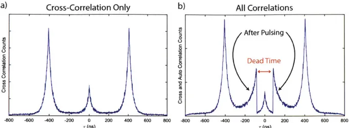
3.2.2 Dead Time
Since the detection of a photon relies on an avalanche of generated carriers in the silicon chip, which can only occur with the detector resting at a reverse bias, SPADs have a significant reset time. Before a detector can record a subsequent photon arrival, all the generated carriers must be swept away and the reverse bias reapplied. This manifests in a many tens of nanoseconds "dead time" when the detector is inactive. Artifacts due to detector dead time are common in photoluminescence measurements, particularly with heterogeneous or defect riddled ensembles or films. Generally, dead time artifacts manifest as a second rise or bump ~80 ns after the original signal rise (Figure 3-4). Most instruments quote a percent maximum count rate of 5% the repetition rate at which there is a high risk of dead time artifacts, but this guideline is not sufficient to avoid artifacts. These numbers assume a fairly constant exponential-like decay which takes most of the laser repetition time to complete. That is to say, the photons are fairly well distributed in time throughout one repetition cycle of the laser. If a sample has a very rapid decay component followed
a) 10 I b ' ' Dead Time 10-2 10-2 0 0 z z 10 10-4 0 100 200 300 -800 -600 -400 -200 0 200 Time (ns) Time (ns)
Figure 3-4 a) PL lifetime data of a solution phase ensemble of emitters with a dead-time artifact in the decay curve.
b) The whole time trace for the data shown in a) showing a large portion of the repetition window without any NC
decay.
emission dynamics, the 5% rule of thumb begins to break down. The data shown in Figure 3-4a was collected well below the quoted threshold for dead time artifacts, but due to the long, fixed laser repetition rate, and relatively short sample lifetime, dead time artifacts are present (Figure 3-4b). For newer generation detector technologies such as SNSPDs, the fact that timing hardware has a dead time too becomes relevant. While a detector may have a dead time on the order of a nanosecond or two, hardware can have dead times of tens of nanoseconds, resulting in the same artifact in the data.
It may be tempting to attempt to mathematically recover the original decay dynamics from a dataset which contains dead time artifacts, but there is no rigorous way to do so. When these issues arise, the dataset in question must be retaken. The multiexponential decay has many different time scales represented, and no fitting of the data after the dead time artifact can recreate the initial trace without a priori knowledge of the sample kinetics. The reason this trace cannot be recreated is due to the information loss that occurs when photons arrive in the intermediate time window after the first photon has been detected but before the detector has reset is completely lost. Trying to estimate the arrival time of these photons applies a user bias to the data and is in no way representative of the true PL decay.
3.2.3 Afterpulsing
While the detector is in the process of sweeping away excess charges, the detector has an increased probability of producing a second current pulse which does not correlate to the arrival of an additional photon. This process is called afterpulsing and results from the residual carrier avalanche triggering enough electron movement to register as sufficient current and be logged as a detection event. The probability of afterpulsing decreases roughly exponentially with time as shown by the detector autocorrelation signal in Figure 3-5. Due to the detector dead time, we cannot observe afterpulsing occurring before 80 ns, but only catch the tail of the decay. This artifact is particularly relevant in second- and third-order correlation measurements. To mitigate the effects of afterpulsing, it is crucial to only consider the first photon that arrives at each channel in a single laser pulse. If an experiment is run at a faster repetition rate, it is also crucial to consider afterpulsing events that may be displayed on successive pulses. In order to guarantee no afterpulsing artifacts are present in a dataset, only cross-correlations between detectors should be considered. This is true for both single-molecule measurements and solution-phase measurements. It is also possible for afterpulsing artifacts to be present in lifetime measurements run at relatively low average count rates. Considering only the first photon arrival per 100 nanoseconds or per