HAL Id: hal-01314704
https://hal.archives-ouvertes.fr/hal-01314704
Submitted on 11 May 2016
HAL is a multi-disciplinary open access archive for the deposit and dissemination of sci-entific research documents, whether they are pub-lished or not. The documents may come from teaching and research institutions in France or abroad, or from public or private research centers.
L’archive ouverte pluridisciplinaire HAL, est destinée au dépôt et à la diffusion de documents scientifiques de niveau recherche, publiés ou non, émanant des établissements d’enseignement et de recherche français ou étrangers, des laboratoires publics ou privés.
Periodic domain patterning by electron beam of proton
exchanged waveguides in lithium niobate
Dmitry Chezganov, Evgenii Vlasov, Maxim Neradovskiy, Lubov Gimadeeva,
Elisaveta Neradovskaia, Maria Chuvakova, H Tronche, F Doutre, P Baldi,
Marc de Micheli, et al.
To cite this version:
Dmitry Chezganov, Evgenii Vlasov, Maxim Neradovskiy, Lubov Gimadeeva, Elisaveta Neradovskaia, et al.. Periodic domain patterning by electron beam of proton exchanged waveguides in lithium niobate. Applied Physics Letters, American Institute of Physics, 2016, 108 (19), pp.192903. �10.1063/1.4949360�. �hal-01314704�
Periodic domain patterning by electron beam of proton
exchanged waveguides in lithium niobate
D.S. Chezganov1,2,a), E.O. Vlasov1, M.M. Neradovskiy1, L.V. Gimadeeva1, E.A. Neradovskaya1, M.A. Chuvakova1, H. Tronche3, F. Doutre3, P. Baldi3, M. P. De Micheli3, V.Ya. Shur1,2
1Institute of Natural Sciences, Ural Federal University, Ekaterinburg, 620000, Russia 2Labfer Ltd., Ekaterinburg, 620014, Russia
3Laboratoire de Physique de la Matière Condensée, University of Nice-Sophia Antipolis, 06100 Nice,
France
Formation of domain structure by electron beam irradiation in congruent lithium
niobate covered by surface dielectric layer with planar and channel waveguides
produced by Soft Proton Exchange (SPE) process has been studied. Formation of
domains with arbitrary shapes as a result of discrete switching has been revealed.
The fact was attributed to ineffective screening of depolarization field in the crystals
presenting a surface layer modified by the SPE process. The dependences of the
domain sizes as a function of the dose and the distance between irradiated areas have
been measured. Finally, we have demonstrated that electron beam patterning using
surface resist layer can produce high quality periodical poling after channel
waveguide fabrication. Second harmonic generation with normalized nonlinear
conversion efficiency up to 48%/(Wcm2) has been achieved in such waveguides.
Periodically poled (PP) nonlinear-optical ferroelectric crystals are widely used for frequency
converters1,2 and various photonic devices.3,4 Lithium niobate (LiNbO3, LN) is one of the
most popular materials for domain engineering due to its large electro-optical and
optical coefficients.5 The ability to combine periodical poling and low-loss waveguides fabrication makes LN a very attractive material for integrated optics.6 Applying an external
electric field (e-field poling) via electrodes is a standard and well developed technique used
to fabricate commercially available periodically poled crystals.7–9 Its main drawback is domain broadening outside the electrode area7 that prevents reaching short periods (< 5 µm). It stimulates development of alternative poling techniques such as electron beam (e-beam)
writting.10 The first realization of e-beam patterning was reported by P.W. Haycock et al11,
who combined e-beam writing with application of an external field at high temperature.
Later, a standard e-beam lithography process was applied to LN for 1D and 2D domain
patterning.12–18 Nevertheless, the random growth of obtained domains resulted in components with low conversion efficiencies.12,13,19 Formation of PPLN by e-beam has been realized in various waveguides, such as He-implanted20 and Ti-diffused19,21–23 ones. Recently, it has been reported that covering the irradiated surface by a thin dielectric layer improves the
quality of e-beam patterning.24–26 Using this technique, we have produced high quality bulk
PPLN in MgO doped LN (MgO:LN).27,28
Proton exchange (PE) is another popular technique for waveguides production in LN.
Waveguides obtained by conventional PE tend to exhibit lower electro-optical29 and nonlinear-optical coefficients30 as well as instability of the refractive index profile.31 The annealed proton exchange (APE) process allows fabricating high optical quality waveguides
with restored coefficients.32,33 Green and blue light generation was demonstrated in PPLN APE waveguides with domain structure produced by e-field patterning.34–36 The highest value of the normalized conversion efficiency was obtained in embedded waveguides produced by
reverse proton exchange (RPE) waveguides.37 Soft Proton Exchange (SPE) is an interesting alternative to get, with one fabrication step only, waveguides presenting a surface index
waveguide is much easily achievable than with RPE waveguides;39 moreover, higher changes of refractive index resulted in less bending losses40 and higher nonlinear efficiency.
Therefore, SPE could be considered as the most attractive process for fabricating nonlinear
integrated optical circuits.
Nevertheless, we have observed that the formation of SPE waveguides in PPLN can lead
to the appearance of uncontrolled nanodomains that perturb the initial periodical structure,
mainly in the Z+ areas, and, therefore, the QPM effect.41 Attempts to create PPLN by e-field
application after SPE have not succeeded due to changes in domain growth resulting in
formation of domain rays.42
In this paper, we present the first detailed study of domain structure formation by e-beam
irradiation in congruent LN (CLN) containing waveguides produced by the SPE process and
covered by e-beam resist layer. Finally, we present an attempt to produce a PPLN channel SPE waveguide using this technique and give some information about the nonlinear results
that will be presented in detail elsewhere.
Starting from Z-cut 0.5-mm thick CLN wafers produced by Gooch & Housego, we
produced planar SPE waveguides on both polar surfaces. The SPE process38 was carried out by dipping the crystal for 72 hours into a benzoic acid bath diluted by 3.1 weight % of
lithium benzoate (BL) and melted at 300°C.
A 100-nm-thick Cu electrode was sputtered on the Z+-polar surface. It was grounded during irradiation. A 2.5-m-thick layer of negative electron-beam resist AZ nlof 2020 Microchemicals was deposited on the Z–-polar surface by spin coating.
The domain patterning was made by irradiation of the Z– surface of CLN with a scanning electron microscope (Auriga Crossbeam workstation, Carl Zeiss) with Schottky field
emission gun. The exposure parameters and beam positioning were controlled by the
the Raith Nanosuite software. Dot (lattice of dots) and stripe (periodic stripe grating)
exposures were used. The e-beam diameter was about 10 nm. The beam position was fixed
for dot exposure. The stripes were defined using a raster-scan covering the desired surface.
The sample was irradiated at accelerating voltage of 10 kV and e-beam current (I) of 1.3 nA.
The irradiation doses (the charge in the incident beam) were defined as Dd = I×t for dot exposure and as DS = I×t/A for stripe exposure, where t is the exposure time and A is the stripe area. The domain patterns were visualized by piezoresponse force microscopy (PFM).
The surface relief of developed resist layer was measured by atomic force microscopy
(AFM).
The formation of periodic stripe domains structure was carried out to fit the e-beam
patterning technique utilizing surface dielectric layer developed by us for periodical poling in
bulk MgO:LN crystals with SPE waveguides.27 Test stripe domain patterns oriented along
Y direction with periods (P) ranging from 3 to 10 μm and irradiated stripe width 0.5 μm were
formed using doses ranging from 0.1 to 1 mC/cm2.
The influence of the dose on the domain patterns at the polar surface visualized by PFM
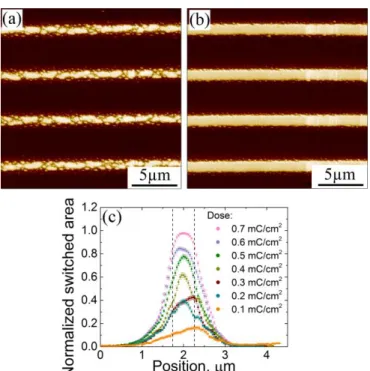
after resist removal was revealed. At low doses (0.1-0.7 mC/cm2) (Fig. 1(a)), submicron domains appear with a normalized switched domain area decreasing from the center to the
border of the irradiated stripe (Fig. 1(c)). Increasing the dose enlarges the switched domain
area due to domains growth and merging (Fig. 1(b)). The formation of continuous stripe
domains was obtained for dose above 0.7 mC/cm2. In all cases, the obtained domains are non-through with their maximum depth up to 150 µm for continuous stripes in the studied
dose range. It is necessary to point out that after e-beam irradiation a number of small
FIG. 1 PFM images of domains appearing after e-beam stripe exposure for different doses: (a) 0.7 mC/cm2, (b) 1 mC/cm2, (c) dependences of the profile of the switched domain area as a function of the charge dose (the dashed lines indicate the area that was exposed by e-beam irradiation).
We have revealed that the domain stripes width varies linearly with the charge dose (Fig. 2(a)):
𝑑(𝐷𝑠) = 𝑑𝑚𝑖𝑛+ 𝐵(𝐷𝑠− 𝐷𝑠,𝑡ℎ), (1)
where dmin is the minimal width of the stripe domain, Ds,th is the threshold dose necessary for
the formation of continuous stripes domain and B is a constant.
The interaction between neighboring domains in the gratings has been studied for doses
larger than 2 mC/cm2. It has been shown that the stripe domain width increases with the period up to 7 m and remains almost constant for the larger periods (Fig. 2(b)).
FIG. 2 The stripe domain width as a function of: (a) the dose for 10-m-period grating, (b) the grating period for a dose of 2 mC/cm2.
The observed evolution of the domain structure with isolated submicron domains
represented the discrete switching caused by ineffective screening of depolarization field in
the ferroelectric with surface dielectric layer produced by SPE process.43 The self-organized domain evolution was demonstrated in LN under highly non-equilibrium switching
conditions, caused by completely ineffective screening of depolarization field, which
prevented the conventional domain growth by sideways wall motion and stimulated
formation of isolated nanodomains.5,44–46 Domain kinetics in this case is governed by
correlated nucleation effect leading to formation of quasi-regular nanodomain structures47–49. It was shown that the averaged period of the domain structure was about the thickness of the
surface dielectric layer produced by PE process.45
Thereby, it is possible to distinguish the main stages of the domain stripes formation:
(1) discrete switching by appearance of isolated submicron-scale domains with decreasing of
the normalized switched domain area from the center to the border of the irradiated stripe;
(2) growing and merging of isolated domains; (3) formation of stripe domains; (4) further
spreading of the stripe domains by sideways wall motion with step generation by merging
with isolated micro- and nano-domains appeared in front of the wall. Such mechanism leads
to continuous wall motion in contrast to jump-like wall motion caused by determined
nucleation observed in the crystals of LN family.50
It should be noted that presence of the resist layer is mandatory for periodical poling of
CLN with SPE planar waveguides. Without this resist layer, it was impossible to create any
domain structure by e-beam irradiation. This fact can be attributed to a fast redistribution of
the space charges caused by the higher conductivity of the SPE layer.
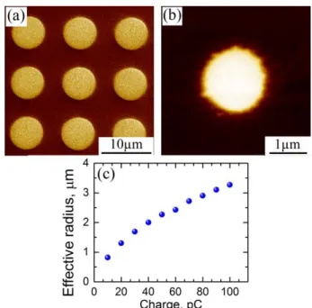
The growth of isolated domains as a function of dot exposure was studied. Several
patterns of 10×10 dots with a 10-m-period were irradiated, with dose increasing from one pattern to the other in the range from 10 to 100 pC. The formation of circular domains on the
irradiated polar surface was revealed by PFM (Fig. 3(a)). The absence of domains on the
opposite polar surface indicated that the domains were non-through. Increasing the dose did
not modify the domain shape. The monotonic nonlinear dependence of domain radius as a
function of the deposited charge is similar to that obtained in MgO:LN without PE layer
(Fig. 3(c)).27 Nevertheless, it is necessary to point out that in the PE crystals the domain size variations in each array are much smaller than those observed in the virgin crystals. The
circular domain shape is a clear demonstration of isotropic domain growth, which was
discussed for stripe domains (Fig. 3(b)).
FIG. 3 PFM image of (a) circular domain array and (b) individual circular domain after dot exposure, (c) dose dependence of domain radius.
Finally, we have demonstrated the possibility to produce stripe domain structures
oriented along the X crystallographic direction (Fig. 4(a)) as well as ring-shaped domain
(Fig. 4(b)). High quality of domain patterns allowed us to claim that the used technique could
be applied to formation of domains with arbitrary shape in SPE waveguides.
The obtained results allowed us to optimize the procedure of obtaining periodically poled
waveguides. Starting from a CLN sample with SPE channel waveguides of different widths
channel waveguides aligned along the X crystallographic axis using the SPE method.
Channels waveguides were photolithographically defined in a 200 nm SiO2 layer deposited
on the Z- surface of the wafer. A planar waveguide was fabricated on the uncovered Z+ surface. Tuning of the irradiation parameters allowed us to control the duty cycle. On the
used equipment, we were able to produce domain patterns by e-beam scanning in the area of
1.5×1.5 mm2. Producing larger PP areas requires moving the sample by stage translation, which introduced some stitching errors due to the limited precision of the used translation
table.
Fig. 4 PFM images of (a) periodic domain stripes oriented along X direction, (b) ring-shaped domain.
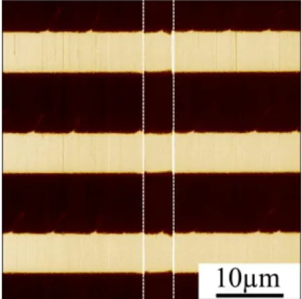
Finally, observation by PFM revealed that the e-beam patterning was nearly not affected
by the presence of the waveguide in contrast to what was observed for electric field poling42 (Fig. 5).
FIG. 5 PFM images of PPLN structure (horizontal) fabricated perpendicular to channel waveguide (vertical) produced by SPE method in CLN: dark – initial domain state, light – switched domains.
We have created PPLN structure in SPE channel waveguide with aspect ratio close to
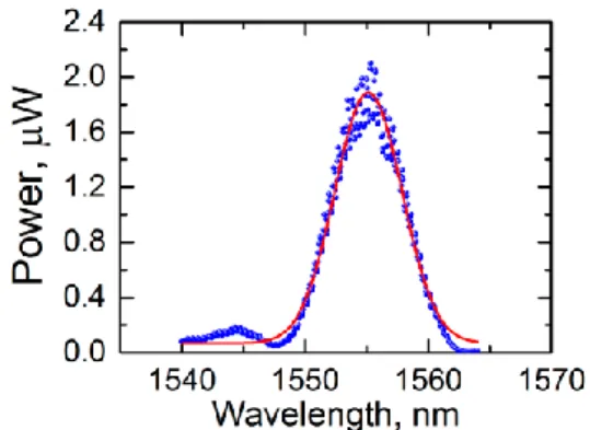
amplifier delivering 100 mW within the wavelength range 1535 to 1570 nm. In Fig. 6, we
plot the power of the SH beam as a function of the pump wavelength, and for 1.5-m-long PP structures we obtained up to 48%/(Wcm2) normalized nonlinear conversion efficiency, which is equal to what is usually reported for surface waveguides with periodical domain
structure created by e-field poling. Almost the same conversion efficiency was observed for
longer domain patterns with FWHM of SHG spectrum being in good agreement with the
theoretically predicted one. The detailed study of these SHG experiments will be published
elsewhere.
FIG. 6 The wavelength dependence of the SHG power for SPE waveguides. Domain pattern period – 16.2 m, length – 1.5 mm. Waveguide width – 8 m.
In summary, we have carried out a detailed study of the formation of periodic domain
structures by e-beam patterning of CLN wafers presenting planar and channel waveguides
produced by SPE process. It has been shown that the use of a resist layer is mandatory to
periodical poling in LN crystal with PE layers. The formation of isolated submicron domains
has been observed and attributed to the discrete switching caused by ineffective screening of
the depolarization field provided by the surface layer modified by SPE process. The
dependences of domain size as a function of dose and period have been obtained. The
formation of arbitrary shaped domains has been demonstrated. The developed technique has
been used to write high quality periodic domains in channel waveguides, which allowed
obtaining a nonlinear conversion efficiency of up to 48%/(Wcm2) in SHG experiments. Therefore, this study shows that it is possible to get state-of-the-art SHG efficiency by
periodic domain patterning after the waveguides fabrication. This is of major interest for
producing devices combining nonlinear sections with more complicated circuits.
The authors would like to acknowledge V. Kvashnin for participation in the experiments,
E. Vaskina, Dr. A.R. Akhmatkhanov, and Dr. D.O. Alikin for technical assistance. The equipment of the Ural Center for Shared Use “Modern nanotechnology” UrFU was used. The research was made possible in part by RFBR (15-32-21102-mol_a_ved), by Government of
the Russian Federation (Act 211, Agreement 02.A03.21.0006), and by President of Russian
Federation grant for young scientists (Contract 14.Y30.16.8441-МК). V.S. acknowledges
financial support within the State Task from the Ministry of Education and Science of the
Russian Federation (Project No. 1366.2014/236).
References
1H.S. Nalwa, Handbook of Advanced Electronic and Photonic Materials and Devices (Acad.
Press, San Diego, Calif., 2001).
2R.L. Byer, J. Nonlinear Opt. Phys. Mater. 6, 549 (1997). 3V. Berger, Phys. Rev. Lett. 81, 4136 (1998).
4N.G.R. Broderick, G.W. Ross, H.L. Offerhaus, D.J. Richardson, and D.C. Hanna, Phys. Rev.
Lett. 84, 4345 (2000).
5V.Ya. Shur, J. Mater. Sci. 41, 199 (2006).
6M. Bazzan and C. Sada, Appl. Phys. Rev. 2, 040603 (2015).
7V.Ya. Shur, E.L. Rumyantsev, E.V. Nikolaeva, E.I. Shishkin, R.G. Batchko, G.D. Miller,
M.M. Fejer, and R.L. Byer, Ferroelectrics 236, 129 (2000).
8R.G. Batchko, V.Ya. Shur, M.M. Fejer, and R.L. Byer, Appl. Phys. Lett. 75, 1673 (1999). 9H. Ishizuki, I. Shoji, and T. Taira, Appl. Phys. Lett. 82, 4062 (2003).
Switching (Springer Berlin Heidelberg, Berlin, Heidelberg, 2008), p. 201.
11P.W. Haycock and P.D. Townsend, Appl. Phys. Lett. 48, 698 (1986). 12H. Ito, C. Takyu, and H. Inaba, Electron. Lett. 27, 1221 (1991).
13A.C.G. Nutt, V. Gopalan, and M.C. Gupta, Appl. Phys. Lett. 60, 2828 (1992).
14J. He, S.H. Tang, Y.Q. Qin, P. Dong, H.Z. Zhang, C.H. Kang, W.X. Sun, and Z.X. Shen, J.
Appl. Phys. 93, 9943 (2003).
15L.S. Kokhanchik, M.N. Palatnikov, and O.B. Shcherbina, Phase Transit. 84, 797 (2011). 16L.S. Kokhanchik and T.R. Volk, Appl. Phys. B 110, 367 (2013).
17L. Mateos, L.E. Bausá, and M.O. Ramírez, Opt. Mater. Express 4, 1077 (2014).
18V.Ya. Shur, D.S. Chezganov, M.M. Smirnov, D.O. Alikin, M.M. Neradovskiy, and D.K.
Kuznetsov, Appl. Phys. Lett. 105, 052908 (2014).
19C. Restoin, C. Darraud-Taupiac, J.-L. Decossas, J.-C. Vareille, V. Couderc, A. Barthélémy,
A. Martinez, and J. Hauden, Appl. Opt. 40, 6056 (2001).
20T.R. Volk, L.S. Kokhanchik, R.V. Gainutdinov, Y.V. Bodnarchuk, S.M. Shandarov, M.V.
Borodin, S.D. Lavrov, Hongliang Liu, and Feng Chen, J. Light. Technol. 33, 4761 (2015).
21X. Wang, Y. Zhou, and C.K. Madsen, J. Light. Technol. 32, 2989 (2014).
22C. Restoin, C. Darraud-Taupiac, J.L. Decossas, J.C. Vareille, J. Hauden, and A. Martinez, J.
Appl. Phys. 88, 6665 (2000).
23L.S. Kokhanchik, M.V. Borodin, S.M. Shandarov, N.I. Burimov, V.V. Shcherbina, and
T.R. Volk, Phys. Solid State 52, 1722 (2010).
24X. Li, K. Terabe, H. Hatano, and K. Kitamura, J. Cryst. Growth 292, 324 (2006). 25X. Li, K. Terabe, H. Hatano, and K. Kitamura, Jpn. J. Appl. Phys. 45, L399 (2006).
26D.S. Chezganov, M.M. Smirnov, D.K. Kuznetsov, and V.Ya. Shur, Ferroelectrics 476, 117
(2015).
106, 232902 (2015).
28D.S. Chezganov, D.K. Kuznetsov, and V.Ya. Shur, "Simulation of spatial distribution of
electric field after electron beam irradiation of MgO-doped LiNbO3 covered by resist layer,"
Ferroelectrics 496, (2016) (accepted for publication).
29R.A. Becker, Appl. Phys. Lett. 43, 131 (1983).
30T. Suhara, H. Tazaki, and H. Nishihara, Electron. Lett. 25, 1326 (1989). 31A. Yi-Yan, Appl. Phys. Lett. 42, 633 (1983).
32P.G. Suchoski, T.K. Findakly, and F.J. Leonberger, Opt. Lett. 13, 1050 (1988).
33X. Cao, R. Srivastava, R.V. Ramaswamy, and J. Natour, IEEE Photonics Technol. Lett. 3,
25 (1991).
34M. Fujimura, T. Suhara, and H. Nishihara, Electron. Lett. 28, 721 (1992).
35M. Fujimura, K. Kintaka, T. Suhara, and H. Nishihara, Electron. Lett. 28, 1868 (1992). 36M. Fujimura, K. Kintaka, T. Suhara, and H. Nishihara, J. Light. Technol. 11, 1360 (1993). 37K.R. Parameswaran, R.K. Route, J.R. Kurz, R.V. Roussev, M.M. Fejer, and M. Fujimura,
Opt. Lett. 27, 179 (2002).
38L. Chanvillard, P. Aschiéri, P. Baldi, D.B. Ostrowsky, M. De Micheli, L. Huang, and D.J.
Bamford, Appl. Phys. Lett. 76, 1089 (2000).
39S.M. Kostritskii, Y.N. Korkishko, V.A. Fedorov, V.P. Mitrokhin, O.G. Sevostyanov, I.M.
Chirkova, O. Stepanenko, and M.P. De. Micheli, J. Eur. Opt. Soc. Rapid Publ. 9, 14055
(2014).
40K. X. Chen, X. P. Li, Y. L. Zheng, and K. S. Chiang, IEEE Photonics Technol. Lett. 27,
1224 (2015).
41M.M. Neradovskiy, V.Ya. Shur, N.A. Naumova, D.O. Alikin, A.I. Lobov, H. Tronche, E.
Quiller, P. Baldi, and M.P. De Micheli, Ferroelectrics 476, 127 (2015).
Tronche, P. Baldi, and M.P. De Micheli, "Investigation of domain kinetics in congruent
lithium niobate modified by proton exchange," Ferroelectrics 496, (2016) (accepted for
publication).
43V.Ya. Shur, A.R. Akhmatkhanov, and I.S. Baturin, Appl. Phys. Rev. 2, 040604 (2015). 44V.Ya. Shur, E. Shishkin, E. Rumyantsev, E. Nikolaeva, A. Shur, R. Batchko, M. Fejer, K.
Gallo, S. Kurimura, K. Terabe, and K. Kitamura, Ferroelectrics 304, 111 (2004).
45M.A. Dolbilov, E.I. Shishkin, V.Ya. Shur, S. Tascu, P. Baldi, and M.P. De Micheli,
Ferroelectrics 398, 108 (2010).
46M.A. Dolbilov, V.Ya. Shur, E.V. Shishkina, E.S. Angudovich, A.D. Ushakov, P. Baldi, and
M.P. De Micheli, Ferroelectrics 442, 82 (2013).
47V.Ya. Shur, D.K. Kuznetsov, A.I. Lobov, E.V. Nikolaeva, M.A. Dolbilov, A.N. Orlov, and
V.V. Osipov, Ferroelectrics 341, 85 (2006).
48V.Ya. Shur, D.K. Kuznetsov, E.A. Mingaliev, E.M. Yakunina, A.I. Lobov, and A.V. Ievlev,
Appl. Phys. Lett. 99, 082901 (2011).
49V.Ya. Shur, D.S. Chezganov, M.S. Nebogatikov, I.S. Baturin, and M.M. Neradovskiy, J.
Appl. Phys. 112, 104113 (2012).