Development of a cluster deposition process
for fabricating quantum dot composite
materials
by
Shih-Tung Ngiam
B.S. Chemical Engineering-Biomedical Engineering Carnegie-Mellon University, 1987
M.S. Chemical Engineering Practice Massachusetts Institute of Technology, 1991
Submitted to the Department of Chemical Engineering in partial fulfillment of the requirements for the degree of
Doctor of Philosophy in Chemical Engineering at the
Massachusetts Institute of Technology June 1996
© Massachusetts Institute of Technology. All rights reserved.
Signature of Author: ... ... hemical Engineering
April 26, 1996
Certifiedby: ...
Professor of Chemical Eng;
Certified by: ... ... .. ... ... ... ... ... ... ... Klavs F. Jensen and Engineering -iesis Supervisor
...
,,n, D. Kolenbrander Associate Professor of Materials Science and Engineering" visor
A ccepted by: ...
Robert E. Cohen Professor of Chemical Engineering Chairman, Committee for Graduate Students
OF TECGHNOLO-GY
JUN 2 71996 Science
Development of a cluster deposition process for
fabricating quantum dot composite materials
by
Shih-Tung Ngiam
submitted to the Department of Chemical Engineering on April 26, 1996, in partial fulfillment of the requirements for the degree of Doctor of Philosophy
in Chemical Engineering
Abstract
Nanstructured composites have been fabricated by codepositing nanoclus-ters into solid host matrices. Ge, Si and Er nanoclusnanoclus-ters were synthesized by Pulsed Laser Ablation-Supersonic Expansion (PLA-SSE) then codeposited into Si or SiOx hosts grown by chemical vapor deposition, laser evaporation or re-active laser evaporation.
Electron microscopy of Ge:Si composites showed that they consisted of Ge nanocrystals surrounded by a Si matrix. Rutherford Backscattering (RBS) analysis indicated a Ge content of 1 atomic percent. X-ray diffraction (XRD) showed that the Si host was polycrystalline. No photoluminescence (PL) was observed from the Ge:Si composites.
The SiOx matrices were sub-stoichiometric because of the formation of mi-cron-scale Si particles within the SiOx host (a consequence of laser evapora-tion), and the low 02 flux during deposition. Oxide- or hydride-passivated PLA-SSE Si clusters exhibit visible PL, but Si:SiOx composites did not exhibit
any PL. This shows that Si clusters in the Si:SiOx composite are poorly passi-vated. Light emission by radiative recombination of excitons is suppressed in
favor of non-radiative recombination at dangling bonds and defects on the surface of the Si cluster.
PL and cathodoluminescence (CL) at 1.54 pm were observed from Er:Si composites, similar to that from other Er-doped systems. The PL intensity falls by half from 4 K to 300 K. This temperature dependence is substantially smaller than that in Er-implanted crystalline Si, and the PL intensity of PLA-SSE Er:Si is greater than that of Er-implanted Si at the same temperature. High concentrations of C and O were detected in PLA-SSE Er:Si composites by Auger spectroscopy and by XPS. Complexes of Er with these two impurities have been shown to be luminescent centers in Er-implanted Si, so the en-hanced PL from PLA-SSE Er:Si composites is most likely due to the presence
of Er-C and Er-O complexes within the laser-evaporated Si matrix rather than to quantum confinement effects in Er nanoclusters.
Thesis Supervisor: Klavs F. Jensen
Title: Professor of Chemical Engineering and Materials Science and Engineering
Thesis Supervisor: Kirk D. Kolenbrander
Table of Contents
List of Figures... 6 L ist of T ables... 13 1 INTRODUCTION...14 1.1 Optoelectronic materials ... 14 1.2 Quantum dots...151.2.1 Quantum confinement and non-linear optics...15
1.2.2 II-VI compound semiconductor quantum dots ... 16
1.2.3 Group IV quantum dots ... 17
1.2.3.1 Si ... 19
1.2.3.2 Ge... ... 20
1.3 Why quantum dot:host codeposition ? ... 20
2 PULSED LASER ABLATION-SUPERSONIC EXPANSION ... 25
2.1 PLA-SSE cluster source ... ... 25
2.1.1 Modelling of the PLA-SSE cluster source...27
2.2 Size selection... 28 2.3 D eposition rate ... 29 2.4 Si nanocluster characterization ... 29 2.4.1 Photoluminescence ... ... 30 2.5 Ge nanocluster characterization ... ... 32 2.5.1 Photoluminescence ... ... 32
3 HOST MATRIX DEPOSITION... ... 38
3.1 Chemical vapor deposition of Si... .... 38
3.1.1 Deposition from disilane ... 38
3.1.2 Enhancement by Ge...40
3.2 Si02 deposition ... 41
3.2.1 Tetraethylorthosilicate(TEOS)...42
3.2.2 Oxidation of silane or disilane ... 43
3.2.3 Physical Vapor Deposition...43
3.2.4 Active vs. passive oxidation of silicon...45
4 Ge NANOCLUSTER:Si HOST COMPOSITES... ... 50
4.1 Deposition system... ... 50
4.3 Macroanalysis ... 58
4.3.1 Rutherford Backscattering Spectrometry...58
4.4.2 X-ray diffraction... 65
4.4 M icroanalysis ... ... 67
4.4.1 Electron Microscopy ... 67
4.5 Photoluminescence ... 70
4.6 Sum m ary ... 73
5 Si NANOCLUSTER:SILICON OXIDE HOST COMPOSITES ... 75
5.1 Silica deposition by oxidation of disilane ... 75
5.2 Reactive Laser Evaporation ... 76
5.2.1 Minimum oxygen flux for complete oxidation ... 78
5.2.1.1 Si flux... ... ... 78
5.2.1.2 Oxygen flux at the substrate ... 79
5.3 Overall film stoichiomery ... 82
5.3.1 Factorial experiments for optimizing film stoichiometry ... 82
5.4 Microstructure ... 86
5.4.1 Chemical bonding...86
5.4.1.1 X-ray Photoelectron Spectroscopy (XPS) ... 86
5.4.1.2 Silicon monoxide structure ... 91
5.4.1.3 Structure of laser evaporated SiOx films ... 92
5.4.1.4 Structure of SiOx films with PLA-SSE Si clusters...95
5.4.2 Crystallinity... ... 96
5.4.2.1 X-ray Diffraction...96
5.4.2.2 Scherrer formula line broadening ... 98
5.4.3 Ex-situ oxidation ... 98
5.4.3.1 Si particle size ... 102
5.5 Photoluminescence ... ... 104
5.5.1 Ex-situ oxidation ... 104
5.6 Importance of surface passivation ... .... 105
5.7 Process improvements ... 105
5.8 Sum m ary ... ... 106
6 Er NANOCLUSTER:Si HOST COMPOSITES ... 110
6.1 Flexibility of PLA-SSE process ... ... 110
6.2 Er-related luminescence ... ... 111
6.3 Double laser ablation process ... 112 6.4 Photoluminescence ... ... 113 6.5 Electron microscopy ... ... 116 6.6 Film composition ... 120 6.7 Luminescence mechanism ... 122 6.8 Suggested w ork... ... 123 6.9 Sum m ary... ... 123 7 SUMMARY ... 126 8 CONCLUSIONS ... 129 APPENDICES ... ... 130
A.1 Disilane deposition system Standard Operating Procedure ... 130
A.2 Kinetic model for silicon deposition from Si2H6 ... 137
A.3 Kinetic model for oxidation of Si particles ... 138
A.3.1 Oxidation of planar Si wafers ... 138
List of Figures
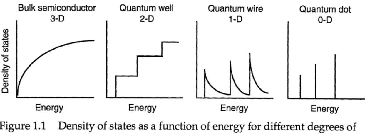
Figure 1.1 Density of states as a function of energy for different degrees ofquantum confinement.
15 Figure 1.2 Change in optical absorption spectra of CdSe nanocrystallites
with decreasing nanocrystallite diameter (from Murray, Norris and Bawendi, 1993)
17 Figure 1.3 Exciton energy as a function of quantum dot radius for Si and Ge.
Right ordinate indicates the confinement energy AE measured from the indirect band-gap energy of the bulk material. (From Takagahara and Takeda, 1992.)
18
Figure 2.1 Schematic diagram of the Pulsed Laser Ablation-Supersonic Expansion cluster source. A pulse of He flows through the growth channel as the rotating target rod is irradiated with a 532 nm laser pulse. Evaporated material is cooled by the flowing He and condenses into a broad range of cluster sizes. The
condensation reaction is then rapidly quenched by the supersonic expansion of He into the primary chamber which is at an
operating pressure of 10-4 torr.
26 Figure 2.2 High Resolution Transmission Electron Microscope image of
PLA-SSE Si nanocrystal collected on C-formvar coated TEM grid (from Werwa et al, 1994).
30 Figure 2.3 Photoluminescence spectrum of Si nanoclusters deposited on
teflon substrate, (a) as-deposited and (b) after dipping in HF.
31
Figure 2.4 Micrographs of Ge nanoparticle collected on C-coated TEM grid at 4000C. Lattice planes are visible in the highlighted area of part (a) and are shown at higher magnification in part (b). The lattice spacing of 1.9 A is close to the reference value of 2.0A for Ge (220)
Figure 2.5 (a) XRD spectrum of PLA-SSE Ge clusters deposited on a Si (100)
wafer. Peaks are seen at 20=- 27.30, 45.30 and 53.70 in curve
corresponding to Ge (JCPDS card 4-545). The feature around 20 = 33.00 is the 800 Si reflection from the single crystal Si wafer
substrate. Curves (b)-(d) are simulated spectra for bulk Ge, 10 nm and 5 nm diameter Ge particles respectively, illustrating the broadening of XRD lines as particle size decreases.
34
Figure 3.1 Arrhenius plot for the reaction Si2H6 + 02 at atmospheric
pressure. Silica is deposited by passing disilane(diluted to 1% in He), 02 and N2 at flow rates of 200, 600 and 1500 cc/min
respectively over a heated Si wafer substrate. Points labelled "Photo CVD" are for photoactivated (low pressure Hg lamp) depositions. (From Mishima et al., 1984)
Figure 3.2 Critical presssure for transition between active and passive oxidation on Si(100). Below the curve, Si is etched by the
formation of gaseous SiO, and above the curve, passive oxidation takes places with the deposition of solid Si0 2.
46 Figure 4.1 Pulsed Laser Ablation-Chemical Vapor Deposition (PLA-CVD)
apparatus. The system consists of two diffusion-pumped vacuum chambers connected through an 8" gate valve with the PLA-SSE cluster source in the primary chamber and the disilane CVD system in the secondary chamber.
51
Figure 4.2 Schematic diagram of Pulsed Laser Ablation- Chemical Vapor Deposition apparatus. Nanoclusters are collected on a heated substrate in the secondary chamber while a silicon matrix is simultaneously deposited using disilane. The working pressure in the secondary chamber is -10-6 torr while the pressure in the primary chamber is ~10-4 torr.
Figure 4.3 Comparison of measured growth rates of Ge cluster:Si host composites to predicted growth rates for deposition of pure Si. The Ge content of the Ge:Si composites is less than 1 atomic percent, and the composites grown at Si2H6 partial pressures of 3-6 x 10⁻⁶ torr. Model predictions were made for Si2H6 partial pressures of 1 x 10⁻⁶ torr and 5 x 10⁻⁶ torr. The standard deviation of step heights across a sample was 15%, and 2a error bars are shown as arrows for each experimental data point.
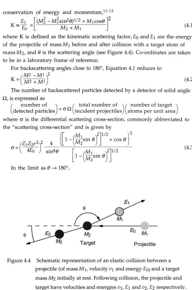
Figure 4.4 Schematic representation of an elastic collision between a projectile (of mass M1, velocity vi and energy Eo) and a target
mass M2 initially at rest. Following collision, the projectile and target have velocities and energies vl, E1 and v2, E2 respectively.
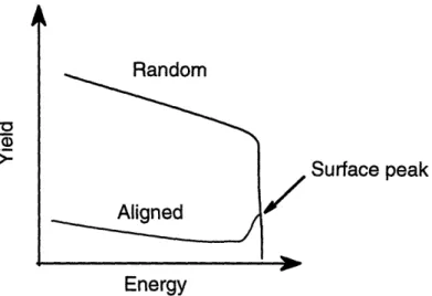
59 Figure 4.5 Schematic representation of channelling effects when a major axis
or plane of a single crystal is aligned along the ion beam. The surface peak is due to scattering from the outermost layer of atoms.
61 Figure 4.6 Random and aligned 2 MeV He+ RBS spectra for Ge nanoclusters
deposited on a Si(100) wafer without a codeposited Si host matrix. Theoretical peak locations for Si and Ge on the surface are
indicated by Esi and EGe respectively. 62
Figure 4.7 Experimental and simulated RBS spectra for Ge:Si composites. Channelled spectra for Ge:Si composites deposited (a) at 7300C for 3 hours, and (b) at 7000C for 8 hours. Simulated spectra for Geo.oosSio.992 films (c) with a Si capping layer, (d) without a Si
cap. 64
Figure 4.8 X-ray diffraction spectrum of Ge:Si composite deposited at 7000C. Bars indicate the position andrelative intensity of diffraction peaks from diamond cubic Si (JCPDS card 27-1402). Additionally there is an 800 reflection from the Si (100) substrate at 33.00
Figure 4.9 STEM images of Ge:Si composite deposited at 5000C on C-coated TEM grid: (a) Annular dark field image; (b) Ge element map; (c) Si element map. The Ge and Si element maps were collected by EDS and represent the same region shown in part (a). Regions of higher Ge or Si density appear darker in parts (b) and (c)
respectively.
68
Figure 4.10 High Resolution Transmission Electron Microscope image of Ge:Si composite grown at 5000C on a C-coated TEM grid. Ge (111) lattice fringes are visible with a spacing of 3.3 A.
69
Figure 4.11 Near infrared photoluminescence spectrum for Ge:Si composite analyzed by RBS prior to PL spectroscopy. The PL behaviour shown is due to radiation-induced centers created by irradiation of the sample with He+ ions during RBS analysis. Ge:Si
composites which were not analyzed by RBS do not exhibit any photoluminescence.
71 Figure 5.1 Double laser ablation and oxidation. The Nd:YAG laser beam is
split into two beams with one beam (25% of the original beam energy) used for PLA-SSE cluster production and another (75 %) used to laser evaporate a second Si rod placed close to the
substrate. Oxygen gas is introduced through a doser and oxidizes
the ablated Si to form a silicon oxide film. 77
Figure 5.2 Si deposition rate as a function of laser power. The Si matrix rod was 3.8 cm away from the quartz crystal monitor sensor head. Laser power is measured before splitting the beam, and
approximately 75 % of the measured beam energy is used to ablate the Si matrix rod. Filled and open circles represent data
taken on two different days. 79
Figure 5.3 Correlation between local oxygen pressure at substrate holder and overall chamber pressure. Local oxygen pressure at the substrate holder is measured with a Fast Ionization Gauge (o) or a thermocouple gauge (x) while the chamber pressure is
measured with an ionization gauge.
Figure 5.4 RBS spectrum of silicon oxide film deposited on (100) Si wafer. Simulated data is for a film with an O/Si ratio of 1.6 and a thickness of 0.5 Cgm. The film was deposited with an oxygen pressure of 5 x 10- 4 torr, a laser fluence of 33 mJ/pulse and a rod-substrate distance of 3.8 cm. E Si and Eo represent the energy of
ions backscattered from Si and 0, respectively, on the surface. 83 Figure 5.5 Results of a series of experiments to determine the effect of
rod-substrate distance, rod-substrate temperature, and laser power on the composition of SiOx films deposited by laser vaporization and oxidation. None of the main effects or interactions were found to
be significant. The 95% confidence interval was 0.44. 84 Figure 5.6 XPS spectrum of Si wafer with native oxide. Two Si 2p peaks are
seen, arising from Si atoms in the oxide layer and in the bulk Si. Spectrum was collected on SSX-100 instrument with monochrom-atized Al Ka( X-rays. Static charge effects were corrected for by setting the adventitious carbon peak (not shown) to 284.6 eV on
the binding energy scale. 90
Figure 5.7 XPS spectrum of SiOx film after smoothing and background subtraction. SiOx film was deposited at room temperature with a laser fluence of 34 mJ/pulse and an oxygen pressure of 1 x 10- 4 torr onto an A1203 substrate. Data were collected on the PE 5100
instrument. 92
Figure 5.8 Si 2p photoelectron spectrum as a function of duration of sputtering with Ar+ ions. The etch rate was approximately 20A/min.
94 Figure 5.9 Ratio of Si4+ to SiO in SiOx, film as a function of sputter time. The
Si4+/SiO ratio was assumed to be equal to the the ratio of the heights of the Si4+ and Siocore-level photoelectron peaks divided
Figure 5.10 X-ray diffraction spectra of SiOx films deposited on fused silica substrates with and without codeposited PLA-SSE Si
nanoclusters. Bars indicate the position andrelative intensity of diffraction peaks from diamond cubic Si (JCPDS card 27-1402). The broad background peak arises from the amorphous fused silica substrate.
Figure 5.11 Comparison of SiOx XRD spectrum to simulated diffraction patterns for Si particles of various sizes. Bottom curve, (a), is that of SiOx following subtraction of the background signal from the fused silica substrate. Remaining curves are simulated spectra for (b) bulk Si and (c) 10 nm, (d) 5 nm and (e) 3 nm diameter Si particles.
Figure 5.12 Time for complete oxidation of a spherical Si particle as a functior of its initial diameter and temperature. Oxidation is carried out in dry 02 at atmospheric pressure.
Figure 5.13 X-ray diffraction spectra for SiOx deposited with Si nanoclusters on a Si wafer following 0, 2 and 5 hours of oxidation at 10000C. XRD signal from the Si (100) single crystal substrate was
suppressed by slightly misorienting the wafer with respect to the diffractometer plane, but some traces of the Si 800 reflection remain around 26 = 330. Diffraction peaks from Si particles in the deposited SiOx film remain even after 5 hours of oxidation. Figure 5.14 SEM micrograph of SiOx film deposited on a Si wafer. The
micron-scale particles are characteristic of laser deposition and are due to liquid droplets hitting the substrate surface.
Figure 6.1 Double laser ablation process for codepositing Er nanoclusters in a Si host matrix. The Nd:YAG laser beam is split into two beams with one beam (25% of the original beam energy) used in the PLA-SSE cluster source and another (75 %) used to laser evaporate a second Si rod placed close to the substrate.
99
100
101
103
Figure 6.2 Photoluminescence spectra of Er:Si composite before and after a 30 minute anneal in Ar at 5000C. Luminescence from C and O impurity centers is eliminated, while Er-related luminescence is enhanced by annealing.
114
Figure 6.3 Integrated PL intensity as a function of annealing temperature. All anneals are carried out in Ar for 30 minutes. PL spectra were collected at 300 K and 4K.
115
Figure 6.4 SEM micrograph of Er:Si composite deposited on a Si wafer at room temperature for 3 hours. Sample is viewed from the edge at an angle of 150, and the open area to the right is a portion of the substrate which was masked during deposition. The striated cones are formed by the rapid solidification of liquid Si droplets, and the discs formed by Si droplets which cool off more slowly. The smaller spheres are most likely Er particles.
116
Figure 6.5 SEM image and EDS element maps of an Er:Si composite deposited at room temperature for 3 hours on a Si substrate.
(a) SEM image; (b) Er L X-ray map; (c) Si K X-ray map. Areas of higher concentration appear brighter in the element maps.
118
Figure 6.6 Cathodoluminescence map and SEM image of Er:Si composite. Light emission is strongest from cones formed by the rapid solidification of liquid Si droplets. The dark spot in the upper left quadrant of part (a) correponds to an Er particle, seen as a bright
sphere in part (b). 119
Figure A.1 Disilane gas handling system 131
Figure A.2 Schematic representation of 02 concentration, c, as a function of radius, r, for a spherical particle undergoing thermal oxidation and consisting of an unreacted Si core surrounded by a Si02 shell.
ci, c* and cg are the concentration of 02 at the Si-SiO2 interface,
gas-solid interface, and bulk gas respectively. 8 is the thickness of
the oxide layer. 140
List of Tables
Table 4.1 RBS parameters for selected elements using 2 MeV He2+ projectiles with a backscattering angle of 1800. All values were calculated using average atomic masses based on the
natural isotopic distributions of the respective elements. 60 Table 5.1 Deposition conditions used in factorial experiment for
Chapter 1
Introduction
This work is motivated by the search for photonic and optoelectronic materials which could overcome some of the limitations of current electronic materials. A promising avenue for this search is the development of
"quantum dots," i.e., materials whose dimensions are comparable to the Bohr radius of electron-hole pairs. Semiconductor quantum dots have been
synthesized by several methods, including Pulsed Laser Ablation-Supersonic Expansion (PLA-SSE), and these quantum dots possess interesting optical properties which may be applicable to the development of optoelectronic and
photonic materials. For practical purposes, the quantum dots should be combined with another material which controls the quantum dot's environment and which is compatible with existing microelectronic processes. This thesis therefore focuses on the codeposition of PLA-SSE quantum dots in Si and SiO2 host matrices.
1.1 Optoelectronic materials
Since the advent of the silicon integrated circuit in the 1960s, the
microelectronics industry has maintained a remarkable pace of technological advance, rapidly increasing the speed and power of computers while
simultaneously reducing their size and cost.1 Fundamental limits of
semiconductor electronics technology are being approached, however, both in terms of size and speed. Photonic, i.e. light-based, devices could provide an
alternative to electronic devices because much higher speeds are theoretically possible than with electronic devices.2 For the promise of photonics to be
realized, a new generation of photonic and optoelectronic materials has to be developed. Optoelectronic materials would be used as interfaces between photonic and electronic systems, similar to III-V devices used today to bridge electronic and optical transmission in fibre-optic communication devices.
Optoelectronic materials would also be used in displays such as light-emitting diodes and flat panel displays.
Bulk semiconductor Quantum well Quantum wire Quantum dot
3-D 2-D 1-D O-D
Energy Energy Energy Energy
Figure 1.1 Density of states as a function of energy for different degrees of quantum confinement.
1.2 Quantum dots
One promising approach to developing optoelectronic and photonic materials has been to use materials in which electrons are confined to a space comparable to the size of electron-hole pairs (excitons). When the material is quantum confined in one-dimension, the electrons are free to move in only two dimensions, and the material is known as a "quantum well." Quantum well devices made of stacks of thin layers of III-V semiconductors are in
commercial production and are used as laser diodes or light emitting diodes.3-6 Materials which are quantum confined in three dimensions are known as "quantum dots" and have been shown in the laboratory to have strongly enhanced non-linear optical properties.7,8 Quantum dot materials are thus
the focus of this research effort.
1.2.1 Quantum confinement and non-linear optics
In a bulk semiconductor, the physical properties are largely determined by the periodic nature of the lattice. This gives rise to the band structure of the semiconductor, the electron effective mass and other properties. For a large crystal the overall shape and size have no effect on the physical properties. As the dimensions of the crystallite are reduced until they become
comparable to the exciton radius, however, the free carriers become "aware"
of the crystal boundaries.9 The electron and hole wavefunctions must go to
the particle-in-a-box solution to the Schr6dinger equation. Discrete molecule-like energy levels are therefore observed in quantum dots rather than
continuous energy levels such as those observed in bulk semiconductors. This is illustrated in Figure 1.1 which shows the change in the density of states as the degree of quantum confinement increases.7,10,11 The density of
states, Z, is dN/dE, where N is the number of states of energy E. In a bulk semiconductor, the density of states varies continuously with electron energy,
Z oc E1/2 . A two-dimensional quantum well is confined in one dimension
and the density of states becomes a step function. A quantum wire is confined in two dimensions and also has sharp steps with Z oc E-1/2 in between the
steps. A zero-dimensional quantum dot is confined in all three dimensions and the density of states separates into a discrete set of energy levels. The sharp density of states with finite magnitudes results in non-linear optical properties such as sharp resonances and saturable absorption which could be utilized in a photonic device such as an optical switch.9,10 Additionally, the
allowed energy levels are size-dependent so the optical properties of quantum dots are tunable by varying the size of the dot.
1.2.2 II-VI compound semiconductor quantum dots
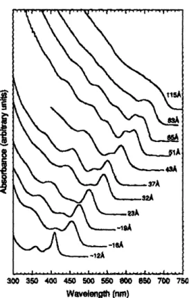
The best developed technique for synthesizing semiconductor quantum dots is probably the controlled precipitation of II-VI compounds in solution developed by Steigerwald, Brus, Bawendi and co-workers.12-15 The size of the
nanocrystallites is controlled by varying the temperature and time of reaction, and then further refined by size-selective precipitation so that size distribut-ions < 5 % r.m.s. in diameter are routinely achieved. Quantum confinement effects are observed in Figure 1.2 which shows the evolution in absorption spectra with size for CdSe nanocrystallites.14 Photoluminescence spectra for
the CdSe nanocrystallites are also size-dependent and blue-shift with decreasing crystallite size.16 This shows that the optical properties of the
quantum dots can be manipulated by controlling the size of the quantum dots.
A key element of this synthesis technique is the presence of capping
groups, e.g., Tri-n-octylphosphine (TOP) /Tri-n-octylphosphine oxide (TOPO), on the surface of the crystallites that control the reaction rate, and hence the size of the crystallites, and also allows for further manipulation of the size
*
8
300 350 400 450 500 560 00 6 50 700 750 Wavelength (nm)
Figure 1.2 Change in optical absorption spectra of CdSe nanocrystallites with decreasing nanocrystallite diameter (from Murray, Norris and Bawendi, 1993)
distribution through the size-selective precipitation step. Photoluminescent and electroluminescent devices have been fabricated from CdSe quantum dots, and the luminescence is tunable by varying the size of the quantum dots.16
1.2.3 Group IV quantum dots
Si and Ge are indirect-gap semiconductors, unlike GaAs and CdSe, which are direct-gap semiconductors. In direct-gap materials the bottom of the conduction band and the top of the valence band lie at k = 0, where k is the crystal momentum.1 7 An excited electron in the conduction band minimum
can spontaneously recombine with a hole in the valence band, emitting a photon of energy equal to the band gap. Direct gap materials are thus efficient light emitters. In indirect-gap materials, however, the conduction band
minimum occurs at k # 0. An electron cannot make a direct transition from 0
the bottom of the conduction band to the top of the valence band because momentum would not be conserved in such a transition. For electron-hole recombination to occur, the momentum of the initial conduction band state must be transferred to the crystal through the creation of a phonon. This three-body event (electron, hole and phonon) is much less likely to occur than a direct electron-hole recombination, so indirect gap materials are very inefficient light emitters. Electrons and holes in Si are thefore more likely to recombine by non-radiative processes (e.g., recombination at defects/deep traps and Auger recombination)1 8 than by radiative processes.
In a quantum dot, the electron and hole wavefunctions are confined in real space so that qualitatively, the wavefunctions spread out in momentum space through the Heisenberg uncertainty relation.19,2 0 Conservation of
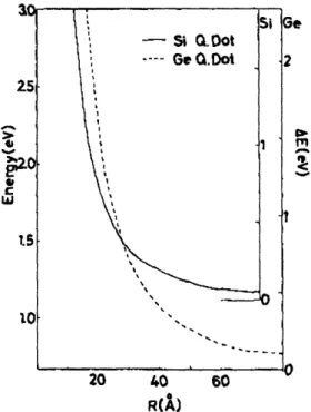
momentum is lifted and Si quantum dots become pseudo-direct gap materials. Si quantum dots could thus become efficient light emitters. In addition, Takagahara and Takeda21 have calculated that the exciton energy in
rI
R(')
Figure 1.3 Exciton energy as a function of quantum dot radius for Si and Ge. Right ordinate indicates the confinement energy AE measured from the indirect band-gap energy of the bulk material. (From Takagahara and Takeda, 1992.)
nanocrystalline Si increases with decreasing crystallite size, as shown in Figure 1.3 Emission from Si could thus takes place in the visible rather than infra-red portion of the spectrum.t This would make quantum confined Si potentially useful as a display material.
1.2.3.1 Si
Visible photoluminescence and electroluminescence have been observed from Si-based materials synthesized by a variety of methods including
electrochemical etching (porous Si),22 aerosol synthesis with size-selective
chromatography,23,24 precipitation from Si-rich glass,25,26 and Pulsed Laser
Ablation-Supersonic Expansion (PLA-SSE).2 7,28 Nanocrystalline Si has been identified as the luminescing center in all these materials, and quantum confinement has been shown to play a role in the mechanism, although the details of the mechanism are still under debate.18 ,2 9,30 The PL behaviour of PLA-SSE Si nanocrystals is substantially similar to that of the Brus material and to porous Si, suggesting a common origin - namely, quantum confined Si, for light emission from all these materials.
For PLA-SSE Si nanocrystals, the photoluminescence peak shifts to lower wavelengths for smaller Si nanocrystals but the spectrum is broad with FWHM - 100 nm due to a wide particle size distribution (see Section 2.4.1) Si nanoclusters were collected directly on TEM grids coated with amorphous carbon and formvar, and examined with a high resolution TEM.19 Figure 2.2
shows a crystalline Si particle approximately 3 nm in diameter. The lattice fringes have a spacing of 1.6
A,
corresponding to the (311) lattice spacing of diamond cubic Si (JCPDS Card 27-1402).50 A wide distribution of particle sizes, with diameters ranging from 2 nm to several hundred nanometers, was also observed.In all of these materials, surface passivation is shown to be essential for enabling photoluminescence from the Si nanocrystallites. Otherwise, non-radiative recombination at surface defects and deep traps will be favoured, and will extinguish the luminescence.18,3 1,32
1.2.3.2 Ge
Like Si, Ge is an indirect gap semiconductor that is ordinarily an
inefficient light emitter.19 Because the effective masses of electrons and holes are smaller in Ge than in Si, the exciton Bohr radius is larger in Ge than in Si.lo Quantum confinement effects are therefore expected to be larger in Ge than in Si for crystallites of the same size (Figure 1.3).21 For example, a
confinement energy of 0.5 eV is calculated for 75A diameter Ge particles but a similar magnitude effect is not seen in Si until the particles are smaller than 45
A.
Photoluminescence has been reported from Ge nanocrystals embedded in SiO2 matrices, synthesized by ion implanting Ge into Si02 or co-sputteringGe and SiO2 then precipitating Ge nanocrystals by heat treatment.33-36 Heath
and co-workers3 7,3 8 have used an inorganic solution-phase technique to synthesize colloids of Ge nanocrystals with sizes ranging from 60-200
A.
Strong size effects are observed in the optical absorption spectra of the Ge nanocrystal colloids, but no photoluminescence has yet been reported.
1.3 Why quantum dot:host codeposition ?
The properties of quantum dots are thus seen to be strongly dependent on their size distribution and degree of surface passivation. In addition, for quantum dots to be integrated into contemporary microelectronic devices, they would have to be compatible with existing semiconductor systems. This would require a means of binding the quantum dots in a film that adheres to semiconductor wafers and that can be fabricated with contemporary
semiconductor processing technology. The matrix material would also have to control the surface chemistry of the quantum dots so that desired
behaviour such as photo- or electroluminescence, is not quenched by parallel non-radiative surface pathways.
These issues have been explored by Danek and co-workers3 9-41 who
synthesized quantum dot:host composites consisting of CdSe quantum dots in a ZnSe matrix. Overcoated quantum dots were synthesized by growing a thin layer of ZnSe around size-selected CdSe nanocrystallites synthesized by the method of Murrary et al.14 The overcoated CdSe quantum dots were then
dispersed into an aerosol using an electrospray apparatus and collected on a heated substrate while a ZnSe film was simultaneously grown by
exhibit optical absorption and photoluminescence spectra similar to those of the CdSe nanocrystallites in solution. However, CdSe:ZnSe composites
synthesized from quantum dots without a pre-deposited ZnSe overlayer have substantially lower PL yields than composites synthesized using overcoated CdSe quantum dots. This indicates that the pre-deposited ZnSe overcoat performs a passivating role that enhances luminescence from the CdSe quantum dots.
In the CdSe:ZnSe system, then, the size of the quantum dots is precisely controlled by the size-selective solution-phase synthesis technique, and surface passivation is controlled by pre-depositing a passivating layer of ZnSe on the CdSe quantum dots prior to their incorporation into the OMCVD-deposited ZnSe matrix.
Present-day microelectronics technology is dominated by silicon, however, so it would be ideal to have a silicon-based quantum dot material so that the wealth of knowledge and investment in silicon processing could be utilized. We propose to use the PLA-SSE method to synthesize a variety of elemental quantum dots and codeposit them into Si matrices, and to synthesize Si quantum dots for codeposition into SiO2 matrices.
The PLA-SSE source is a vacuum-based system and produces bare clusters
in vacuo without any capping groups on the cluster surface. This eliminates
the requirement that the host matrix deposition technique be compatible with the capping group and gives us maximum flexibility to use any vacuum-compatible deposition technique for growing the host matrix, and for investigating questions of cluster surface passivation.
Among the issues that are raised in this work are the sharpness of the interface between nanocluster and host, the likelihood of achieving three-dimensional epitaxy, the passivation of the interface and the effect of the nanoclusters on the matrix film growth.
Given the very small length scales involved, will the quantum dots retain their identity after codeposition into the host, or will they interdiffuse with the host matrix? For codeposition of Ge clusters into a Si host matrix, the two materials are lattice mismatched, but in the case of planar heteroepitaxy, say in the growth of quantum wells, lattice coherency is retained for layers
thinner than the critical thickness. Is there a corresponding critical radius for Si layers grown around Ge nanocrystals? How thick a Si shell could be grown around a Ge nanocrystal before dislocations occur? Passivation of the
quantum dot surface has been shown to be necessary for quantum
confinement effects to be manifested. Will it be possible to eliminate surface defects and dangling bonds on PLA-SSE nanoclusters as they are deposited into the Si and Si02 host matrices? Nanometer-scale seed crystals have been
shown to enhance the growth rate of polycrystalline Si42. Would the PLA-SSE
nanoclusters have a similar effect on the deposition of the Si and SiO2 host matrices ?
Another interesting issue is the effect of the nanocluster size distribution on the properties of cluster:host composites. Size-selection is being
investigated by other workers in the Kolenbrander research group,43 but is
not directly addressed in this thesis. The primary focus of this thesis is on methods of matrix codeposition and surface passivation of the PLA-SSE quantum dots.
In Chapter 2, I describe the PLA-SSE nanocluster source and review
previous characterization of Si and Ge quantum dots synthesized by the PLA-SSE technique. Chapter 3 provides a review of techniques used for depositing Si and SiO2, and in Chapters 4 and 5, I describe the combination of PLA-SSE
with various host matrix deposition techniques for synthesizing quantum dot:host composites. Chapter 4 focuses on composites based on Ge quantum dots while Chapter 5 focuses on materials based on Si quantum dots. Chapter 6 deals with Er-based composites, and Chapters 7 and 8 summarize the work performed for this thesis and its key conclusions.
REFERENCES
1. B. E. Deal and J. M. Early, "The evolution of silicon semiconductor technology: 1952-1977," J. Electrochem. Soc. 126 (1), 20C (1979).
2. E. Abraham, C. T. Seaton, and S. D. Smith, "The optical computer," Sci. Am. 248 (February), 85 (1983).
3. A. Y. Cho, "Twenty years of molecular beam epitaxy," J. Cryst. Growth 150 (1), 1 (1995). 4. D. S. Chemla, "Nonlinear optics in quantum confined structures," Phys. Today 46 (June),
46 (1993).
5. H. S. Hinton, "Switching to photonics," IEEE Spectr. 29 (February), 42 (1992). 6. K. Werner, "Higher visibility for LEDs," IEEE Spectr. 31 (July), 30 (1994). 7. E. Corcoran, "Diminishing Dimensions," Sci. Am. 263 (November), 122 (1990). 8. M. A. Reed, "Quantum Dots," Sci. Am. 268 (January), 118 (1993).
9. P. Horan and W. Blau, "Linear and nonlinear optical properties of semiconductor particles," Phase Transit. 24-26, 605 (1990).
10. A. D. Yoffe, "Low-dimensional systems: quantum size effects and electronic properties of semiconductor microcrystallites (zero-dimensional systems) and some quasi-two-dimensional systems," Adv. Phys. 42 (2), 173 (1993).
11. B. K. Rao, S. N. Khanna, and P. Jena, "Clusters-A new phase of matter," Phase Transit. 24-26, 35 (1990).
12. M. L. Steigerwald and L. E. Brus, "Synthesis, stabilization, and electronic structure of quantum semiconductor nanoclusters," Annu. Rev. Mater. Sci. 19, 471 (1989).
13. M. G. Bawendi, M. L. Steigerwald, and L. E. Brus, "The quantum mechanics of larger semiconductor clusters (quantum dots)," Annu. Rev. Phys. Chem. 41, 477 (1990). 14. C. B. Murray, D. J. Norris, and M. G. Bawendi, "Synthesis and Characterization of
Nearly Monodisperse CdE (E = S, Se, Te) Semiconductor Nanocrystallites," J. Am. Chem. Soc. 115, 8706 (1993).
15. D. J. Norris, M. Nirmal, C. B. Murray, A. Sacra, and M. G. Bawendi, "Size Dependent
Optical Spectroscopy of II-VI Semiconductor Nanocrystallites (Quantum Dots)," Z. Phys. D 26 (1-4), 355 (1993).
16. B. O. Dabboussi, M. G. Bawendi, O. Onitsuka, and M. F. Rubner, "Electroluminescence from CdSe quantum dot/polymer composites," Appl. Phys. Lett. 66 (11), 1316 (1995).
17. M. A. Omar, Elementary solid state physics (Addison-Wesley, Reading, MA, 1975).
18. L. E. Brus, P. F. Szajowski, W. L. Wilson, T. D. Harris, S. Schuppler, and P. H. Citron, "Electronic spectroscopy and photophysics of Si nanocrystals: Relationships to bulk c-Si and porous c-Si," J. Am. Chem. Soc. 117, 2915 (1995).
19. S. S. Iyer and Y. H. Xie, "Light emission from silicon," Science 260, 40 (1993).
20. M. S. Hybertson, "Absorption and emission of light in nanoscale silicon structures," Phys. Rev. Lett. 72 (10), 1514 (1994).
21. T. Takagahara and K. Takeda, "Theory of the quantum confinement effect on excitons in quantum dots of indirect-gap materials," Phys. Rev. B 46 (23), 15578 (1992).
22. L. T. Canham, "Silicon quantum wire array fabrication by electrochemical and chemical dissolution of wafers," Appl. Phys. Lett. 57 (10), 1046 (1990).
23. K. A. Littau, P. J. Szajowski, A. J. Muller, A. R. Kortan, and L. E. Brus, "A luminescent silicon nanocrystal colloid via a high-temperature aerosol reaction," J. Phys. Chem. 97, 1224 (1993).
24. W. L. Wilson, P. F. Szajowksi, and L. E. Brus, "Quantum confinement in size-selected surface-oxidized silicon nanocrystals," Science 262, 1242 (1993).
25. S. Hayashi, S. Tanimoto, and K. Yamamoto, "Analysis of surface oxides of
gas-evaporated Si small particles with infrared spectroscopy, high-resolution electron microscopy, and x-ray photoemission spectroscopy," J. Appl. Phys. 68 (10), 5300 (1990).
26. K. Kohno, Y. Osaka, F. Toyomura, and H. Katayama, "Photoluminescence of Si
microscrystals embedded in SiO2 glass films," Jpn. J. Appl. Phys. 33 (Part 1) (12A), 6616 (1994).
27. L. A. Chiu, A. A. Seraphin, and K. D. Kolenbrander, "Gas phase synthesis and
processing of silicon nanocrystallites: Characterization by photoluminescence emission spectroscopy," J. Electron. Mater. 23 (3), 347 (1994).
28. E. Werwa, A. A. Seraphin, L. A. Chiu, C. Zhou, and K. D. Kolenbrander, "Synthesis
and processing of silicon nanocrystallites using a pulsed laser ablation supersonic expansion method," Appl. Phys. Lett. 64 (14), 1821 (1994).
29. A. G. Cullis and L. T. Canham, "Visible light emission due to quantum size effects in highly porous crystalline silicon," Nature 353, 335 (1991).
30. Y. Kanemitsu, "Luminescence properties of nanometer-sized Si crystallites: Core and surface states," Phys. Rev. B 49 (23), 16845 (1994).
31. A. A. Seraphin, E. Werwa, L. A. Chiu, and K. D. Kolebrander, "The enabling role of
surface passivation in visible photoluminescence from Si nanoparticles," in Interface
control of electrical, chemical and mechanical properties, edited by S. P. Murarka, K.
Rose, T. Ohmi, and T. Seidel (Materials Research Society, Pittsburgh, PA, 1994), p. 433.
32. A. A. Seraphin, S.-T. Ngiam, and K. D. Kolenbrander, "Control of silicon
nanocrystallite luminescence behavior through surface treatments," in Materials
Research Society symposia proceedings, edited by R. C. Cammarata (Materials
33. Y. Maeda, N. Tsukamoto, Y. Yazawa, Y. Kanemitsu, and Y. Masumoto, "Visible photoluminescence of Ge microcrystals embedded in SiO2 glassy matrices," 59, 3168
(1991).
34. Y. Kanemitsu, H. Uto, Y. Masumoto, and Y. Maeda, "On the origin of visible
photoluminescence in nanometer-size Ge crystallites," Appl. Phys. Lett. 61, 2187 (1992). 35. Y. Maeda, "Visible photoluminescence fron nanocrystallite Ge embedded in a glassy
SiO2 matrix: Evidence in support of the quantum-confinement mechanism," Phys. Rev. B
51 (3), 1658 (1995).
36. K. V. Shcheglov, C. M. Yang, K. J. Vahala, and H. A. Atwater, "Electroluminescence and photoluminescence of Ge-implanted Si/SiO2/Si structures," Appl. Phys. Lett. 66
(6), 745 (1995).
37. J. R. Heath and F. K. LeGoues, "A liquid solution synthesis of single crystal germanium quantum wires," Chem. Phys. Lett. 208 (3,4), 263 (1993).
38. J. R. Heath, J. J. Shiang, and A. P. Alivisatos, "Germanium quantum dots: optical properties and synthesis," J. Chem. Phys. 101 (2), 1607 (1994).
39. M. Danek, K. F. Jensen, C. B. Murray, and M. G. Bawendi, "Preparation of II-VI quantum dot composites by electrospray organometallic chemical vapor deposition," J. Cryst. Growth (1994).
40. M. Danek, K. F. Jensen, C. B. Murray, and M. G. Bawendi, "Electrospray organometallic chemical vapor deposition -A novel technique for preparation of II-VI quantum dot composites," Appl. Phys. Lett. 65 (22), 2795 (1994).
41. M. Danek, "Chemical approaches to organometallic chemical vapor deposition of wide band-gap II-VI layers and nanocrystal composites," PhD. thesis, Massachusetts
Institute of Technology, 1995.
42. J. R. Heath, S. M. Gates, and C. A. Chess, "Nanocrystal seeding: A low temperature route to polycrystalline Si films," Appl. Phys. Lett. 64 (26), 3569 (1994).
43. E. Werwa and K. D. Kolenbrander, "Synthesis of thin films of size-selected silicon nanocrystallites using pulsed laser ablation supersonic expansion," presented at the Materials Research Society Fall Meeting, Boston, MA, 1995 (unpublished).
Chapter 2
Pulsed Laser Ablation-Supersonic Expansion
Nanoclusters produced by Pulsed Laser Ablation-Supersonic Expansion (PLA-SSE) are at the core of this research work. This chapter describes the PLA-SSE process, and Si and Ge nanoclusters produced in the system.t The cluster production rate is on the order of 102 ng/cm2 hr, and a wide range of cluster sizes is produced, ranging from particles with a diameter of hundreds of nanometers to diatomic clusters. PLA-SSE is shown to produce nanometer-scale Si and Ge crystals. Whereas bulk Si is a poor light emitter, visible
orange-red photoluminescence is observed from PLA-SSE Si nanoclusters. This is above the band-gap of bulk Si and the blue-shift is believed to be due to quantum confinement effects in Si nanocrystallites.
2.1 PLA-SSE cluster source
Nanoclusters are generated in the gas phase using a Pulsed Laser Ablation-Supersonic Expansion (PLA-SSE) system.1 This system is a descendant of cluster sources developed by Richard Smalley and co-workers at Rice University2 ,3 and also used by Mandich and co-workers at A. T. & T. Bell Laboratories.4 ,5 Cluster sources of this design first appeared in the early 1980s and were initially used to study the structure and reactivity of clusters of < 100 atoms. Fullerenes, e.g., C60, were discovered by Smalley's group in 1985 using a PLA-SSE apparatus.6 Briefly, a pulsed laser beam is used to rapidly heat a solid target and generate a vapor which is rapidly cooled by a synchronized gust of helium flowing over the target. The vapor condenses into multi-atom clusters which are carried into a vacuum chamber by the He gas which
experiences rapid adiabatic cooling as it expands into the vaccum. The condensed clusters are rapidly cooled as well and the condensation process arrested, preventing further growth of the clusters.
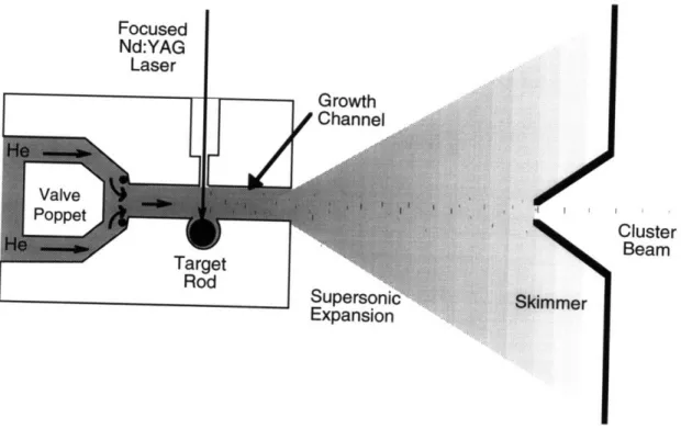
Our PLA-SSE cluster source is shown schematically in Figure 2.1 The 1/4 inch diameter target rod is rotated by mechanical connection to a motor-driven screw and is located along the side of a 1 mm diameter channel drilled
t Characterization of PLA-SSE Si nanoclusters was primarily performed by Chuxin Zhou, Leon Chiu, Arun Seraphin and Eric Werwa of the Kolenbrander research group.
Cluster Beam
Figure 2.1 Schematic diagram of the Pulsed Laser Ablation-Supersonic Expansion cluster source. A pulse of He flows through the growth channel as the rotating target rod is irradiated with a 532 nm laser pulse. Evaporated material is cooled by the flowing He and condenses into a broad range of cluster sizes. The
condensation reaction is then rapidly quenched by the supersonic expansion of He into the primary chamber which is at an
operating pressure of 10-4 torr.
through a 1/4 inch thick stainless steel block. The target rod is ablated with a
Continuum NY60 Neodynium-doped Yttrium Aluminum Garnet (Nd:YAG) pulsed laser focused onto the surface of the target rod and delivering 3-10 mJ/pulse at 20 Hz onto an approximately 0.7 mm diamter spot, corresponding to a power density of 15-50 W/cm2
. Helium gas is pulsed into the growth channel from a 550 psi reservoir, through a General Valves Corporation Series 9 high-speed solenoid valve with a nominal pulse width of 100 Is.
Laser-ablated material from the target is cooled by the He pulse and starts to condense in the growth channel.2
The cluster condensation reactions are then rapidly quenched as the He undergoes a supersonic free jet expansion
into the 10-4 torr vacuum of the primary chamber. A broad distribution of
cluster sizes is produced, ranging from diatomic clusters to large clusters hundreds of nanometers in diameter. This cluster size distribution may be controlled by varying the operating conditions of the PLA cluster source. For example, increasing the length of the growth channel, or increasing the delay between the helium and laser pulses, increases the average size of the
clusters.1 Hopkins et al. have also found that the clustering process is
influenced by the gas pressure behind the nozzle and the laser fluence.2 The
exact mechanism of nanocluster growth in PLA-SSE is still unclear, however, and it is likely that a variety of processes, including homogeneous and
heterogeneous nucleation, condensation, coagulation and agglomeration 7-10)
are at work. Some clusters may also be formed directly by the ejection of solid fragments or liquid droplets from the target rod as a result of laser ablation.
2.1.1 Modelling of the PLA-SSE cluster source
The He pressure behind the nozzle is - 30,000 torr (550 psi) while the background pressure in the vacuum chambers is 10-4 - 10-6 torr. The
Knudsen number (i.e., the ratio of mean free path to characteristic length scale) in our system ranges from << 10-2 in the growth channel to - 103 in the
vacuum chamber. The entire range of flow regimes from continuum to transition to collisionless flow is therefore encountered in the PLA-SSE process.
In the continuum regime (Kn < 0.1), the gas behaves as a viscous fluid and can be modelled using the Navier-Stokes equations. At the other extreme, in
the collisionless or free molecular limit (Kn -4 oo), intermolecular collisions
become very rare and flow is dominated by gas-surface interactions. Gas flow in this regime is typically modelled using test particle Monte Carlo
techniques.11,12 Between these two limits, in the transition regime, the Direct
Simulation Monte Carlo (DSMC) technique is used to model gas flow.13 Individual components of the PLA-SSE process have previously been modelled by other workers in the field. For example, Singh et al.14 have
modelled laser ablation and plasma plume formation using continuum models. Steady-state free jet expansions and supersonic beam skimmers have been extensively studied by Bird15 and Boyd16 using the DSMC method. The
growth channel also bear some similarity to shock tube techniques used in chemical kinetic studies.17
Simulation of the PLA-SSE process is complicated by the transient nature of the process, the unknown composition and reactivity of neutral and ionized species ejected from the target during laser ablation, and the range of flow regimes involved. In addition, Hopkins et al.2 have found that the
mechanical response of the high speed valve also influences cluster
formation, so the valve behavior would also have to be incorporated into a detailed model of the PLA-SSE process.
A greater understanding of the cluster size and velocity distribution would contribute to current efforts to size-select clusters based on velocity slip
between larger and smaller clusters, and to optimize the PLA-SSE cluster source. Unfortunately, the knowledge that could be gained from the simulation would be limited by the large number of assumptions and simplifications required to make the simulation problem tractable. It was therefore felt that the cost of developing a detailed simulation of the PLA-SSE process could not be justified by the returns.
2.2 Size selection
A wide range of particle sizes is produced by the PLA-SSE cluster source, ranging from monatomic and polyatomic species to nanometer-scale clusters and micron-scale particles. A limited degree of control is obtained by varying the length of the growth channel and the timing of the helium and laser pulses, as evidenced by changes in the size-dependent PL spectra of Si clusters as these parameters are varied.18 A very wide size distribution is still
produced, however, as seen by TEM analysis and by the width of the PL peak. Ideally, we would like to be able to control the average size as well as the range of sizes of the clusters.
One approach to this problem is to take advantage of the phenomenon of velocity slip, which results in lighter clusters having a higher velocity than heavier clusters.19,2 0 A cluster packet is produced by each laser pulse, within
which the lighter clusters have a higher velocity than the the heavier
clusters. A velocity filter such as a mechanical chopper wheel which separates the clusters on the basis of velocity will therefore also yield a size separation. Early results in this avenue show that it is possible to shift the peak PL
wavelength of Si clusters from 670 nm to 550 nm using a rotating chopper wheel, and that the FWHM of the PL peak is halved by size-separating the Si clusters.20
2.3 Deposition rate
The deposition rate was measured with a quartz crystal monitor placed 24 cm away from the nozzle along the center-line of the apparatus. The
deposition rate for Si nanocrystals was approximately 250 ng/cm2 hr while
that for Ge nanocrystals was approximately 150 ng/cm2 hr with a laser power
of 5 mJ/pulse. The heat of vaporization of Ge is one-third that of Si on a mass basis, and the boiling point of Ge is also lower than that of Si, so the cluster production rate cannot be inversely proportional to heat of vaporization and boiling point, otherwise the Ge cluster production rate would be expected to be larger than that for Si. Other factors such as the absorptivity and thermal conductivity of the target may thus be controlling the cluster production rate. The relative timing of the laser and helium pulses may also affect the cluster production rate. The same timing was used for Si and Ge, however, and this may have been sub-optimal for Ge, resulting in a lower production rate compared to Si.
Assuming that the angular distribution of clusters leaving the PLA-SSE source is described by a cosine law, the deposition rate 6.3 cm above the center-line (horizontal separation remaining at 24 cm) is predicted to be 87% of the center-line value.21 For a spherical distribution, the deposition rate
would be expected to be 92% of the center-line value. The measured deposition rate, however, is 200 ng/cm2 hr, or only 80% of the center-line
value. The angular distribution of clusters is thus even more strongly
forward peaked than a cosine distribution and falls off rapidly with displace-ment from the center-line.
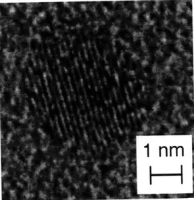
2.4 Si nanocluster characterization
Si nanoclusters were collected directly on TEM grids coated with amorphous carbon and formvar, and examined with a high resolution TEM.22 Figure 2.2 shows a crystalline Si particle approximately 3 nm in diameter. The lattice fringes have a spacing of 1.6
A,
corresponding to the (311) lattice spacing of diamond cubic Si (JCPDS Card 27-1402).23 A wideFigure 2.2 High Resolution Transmission Electron Microscope image of PLA-SSE Si nanocrystal collected on C-formvar coated TEM grid
(from Werwa et al, 1994).
distribution of particle sizes, with diameters ranging from 2 nm to several hundred nanometers, was also observed.
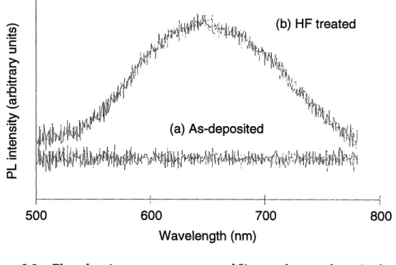
2.4.1 Photoluminescence
PLA-SSE nanoclusters exhibit visible orange photoluminescence under ultraviolet excitation (Figure 2.3). Curve (a) shows that no PL is observed from clusters immediately after deposition, while curve (b) shows the PL spectrum following a 60 s dip in 48 % hydrofluoric acid. The PL spectrum is similar to that observed from electrochemically-etched porous silicon and
nanocrystalline silicon synthesized by an aerosol process.24,25 PLA-SSE Si nanoclusters do not exhibit PL in the gas phase prior to deposition, nor do they exhibit PL when deposited on a solid substrate and allowed to age in
vacuo. PL is only observed when the Si nanoclusters are aged in air or dipped
in HF or HNO3.2 6
An oxide layer is formed on the surface of the Si nanoclusters following atmospheric oxidation or oxidation in HNO3, while a hydride adlayer is formed by dipping in HF. These oxide and hydride layers passivate the Si nanoclusters and allow PL to be observed. In the absence of these treatments,
C13 CU L. CICd c)r C -J a-500 600 700 800
Wavelength (nm)
Figure 2.3 Photoluminescence spectrum of Si nanoclusters deposited on teflon substrate, (a) as-deposited and (b) after dipping in HF.
quenches photoluminescence by providing alternative non-radiative pathways for exciton recombination.
The peak wavelength of the PL can be varied by adjusting the operating conditions of the source to generate larger or smaller clusters.1 The peak
wavelength is also blue-shifted by successive etches in HF or HNO3 due to the
reduction in particle size with each etch cycle. This size-dependence of the PL peak wavelength is similar to that observed by Wilson et al.27 for
aerosol-synthesized Si nanocrystals and indicates that the photoluminescence is due to quantum confinement effects.
Quantum confinement alone is not sufficient to activate photoluminesce-nce from Si nanocrystals, however. Radiative recombination competes with non-radiative recombination and the non-radiative pathways must be
suppressed for luminescence to be observed. For example, defects or dangling bonds at the surface of the nanocrystallite create states within the band gap
that trap carriers and prevent radiative recombination.28 Surface passivation
by oxide or hydride species that tie up dangling bonds is therefore necessary to enable photoluminescence from the Si nanoclusters. Both quantum
confinement and surface passivation must therefore be present for luminescence to be observed from nanocrystalline Si.29
2.5 Ge nanocluster characterization
Ge nanoclusters were collected in the secondary chamber on a C-coated TEM grid heated to 4000C. The TEM grid was heated so that the Ge
nanoclusters collected under these conditions could be compared to the Ge cluster:Si host composites described in Section 4, which are grown on a heated substrate. Particles from 5 to 500 nm in diameter were observed with a 200 kV Akashi EM 002B High Resolution Transmission Electron Microscope
(HREM), but we did not further characterize the size distribution. Diffraction planes are visible in the 10 nm diameter particle shown in Figure 2.4,
indicating that some of the particles are crystalline. The lattice planes had a spacing of 1.9
A,
which is reasonably close to the standard value of 2.0A
for Ge (220) planes (JCPS card 4-0545).23The X-ray diffraction spectrum of Ge clusters collected on a Si wafer are shown in curve (a) of Figure 2.5 The spectrum was collected on a Rigaku RU 300 diffractometer using Cu Ka radiation. Three peaks are seen at 20 = 27.30,
45.30 and 53.70, corresponding to the 111, 220 and 311 reflections of Ge (JCPDS card 4-545). In addition, Bragg diffraction from Si (800) planes in the Si (100) substrate give rise to the strong peak around 33.00.
The calculated effects of finite particle size on the XRD line width are shown in curves (b) - (d), which show simulated XRD spectra for bulk Ge, 10 nm and 5 nm diameter Ge particles, respectively (The theory of X-ray
diffraction is discussed further in Section 5.4.2) The widths of the Ge
diffraction peaks are essentially the same as that for bulk Ge, indicating that some of the Ge particles present are larger than 100 nm in diameter. The HREM images and XRD data therefore show that a very wide particle size distribution is obtained by PLA-SSE, ranging from smaller than 10 nm to several hundred nanometers in diameter.
2.5.1 Photoluminescence
Visible PL spectra were collected by excitation with a tripled Nd:YAG laser (355 nm) using a 0.25 m monochromator and a Si detector. Near infra-red PL spectra were collected by excitation with an Ar+ laser (488 nm) using a 0.75 m
0 5 I I nm 0 1 2 I I I nm
Micrographs of Ge nanoparticle collected on C-coated TEM grid at 4000C. Lattice planes are visible in the highlighted area of part
(a) and are shown at higher magnification in part (b). The lattice spacing of 1.9 A is close to the reference value of 2.0A for Ge (220) planes (JCPDS Card 4-0545).
(a)
(b)
f7~e111 ~ II
25 30 35 40 45
28 (degrees)
50 55 60
(a) XRD spectrum of PLA-SSE Ge clusters deposited on a Si (100)
wafer. Peaks are seen at 20- 27.30, 45.30 and 53.70 in curve
corresponding to Ge (JCPDS card 4-545). The feature around 20= 33.00 is the 800 Si reflection from the single crystal Si wafer
substrate. Curves (b)-(d) are simulated spectra for bulk Ge, 10 nm and 5 nm diameter Ge particles respectively, illustrating the broadening of XRD lines as particle size decreases.
monochromator and a Ge detector. No visible or infra-red PL was detected from the Ge clusters, however, despite theoretical predictions that quantum confinement effects in Ge are even stronger than in Si.30 Unlike Si, however,
Ge is not passivated by its oxide3 1, so PL might not be observed in PLA-SSE Ge
nanoclusters because of the high density of states at the interface. Non-radiative recombination at the surface is then favored and luminescence is
quenched.
Heath32-34 has reported evidence of size-dependence in the extinction
spectra of colloids of Ge nanocrystals in acetonitrile, but has not reported any photoluminescence behaviour. There have been several reports of visible PL from Ge-implanted SiO235,36 and H2-reduced Si-Ge oxides3 7 where the
photoluminescence is attributed to quantum-confined nanocrystalline Ge. The reported PL spectra are remarkably similar to that of silica glass, however, so the PL may in fact be due to SiO 2.
On a historical note, Ge was in fact the earliest semiconductor transistor material and was only replaced by Si in the 1960s due to the rise of planar processing technologies which gave Si the advantage because Si has a robust, easily grown oxide that ties up dangling bonds on the surface and provides excellent surface passivation. The interface trap density on Ge is several orders of magnitude larger than for Si-SiO 2 systems31, and Ge oxides are
water-soluble. This makes the Ge-GeO2 sytem unsuitable for aqueous etching steps and further degrades the interface quality in humid atmospheres.
The factors that made Si the premier material for microlectronic
applications also apply in the field of nanoscale quantum dots. Si nanocrystals synthesized by a variety of techniques are physically protected and chemically and electronically passivated by an SiO 2 layer grown by thermal oxidation or
by spontaneous oxidation in air. Ge nanocrystals, in contrast, are not passivated by their oxide and even if their energy levels were modified by quantum confinement, this is not manifested as photoluminescence because of non-radiative recombination at the Ge cluster surface.
REFERENCES
1. L. A. Chiu, A. A. Seraphin, and K. D. Kolenbrander, "Gas phase synthesis and
processing of silicon nanocrystallites: Characterization by photoluminescence emission spectroscopy," J. Electron. Mater. 23 (3), 347 (1994).